EP0368625A2 - Verfahren und Gerät zur Bildung eines Pattern-Layouts einer integrierten Halbleiterschaltung - Google Patents
Verfahren und Gerät zur Bildung eines Pattern-Layouts einer integrierten Halbleiterschaltung Download PDFInfo
- Publication number
- EP0368625A2 EP0368625A2 EP89311525A EP89311525A EP0368625A2 EP 0368625 A2 EP0368625 A2 EP 0368625A2 EP 89311525 A EP89311525 A EP 89311525A EP 89311525 A EP89311525 A EP 89311525A EP 0368625 A2 EP0368625 A2 EP 0368625A2
- Authority
- EP
- European Patent Office
- Prior art keywords
- layout pattern
- transistor
- forming
- existing
- integrated circuit
- Prior art date
- Legal status (The legal status is an assumption and is not a legal conclusion. Google has not performed a legal analysis and makes no representation as to the accuracy of the status listed.)
- Granted
Links
Images


Classifications
-
- H—ELECTRICITY
- H10—SEMICONDUCTOR DEVICES; ELECTRIC SOLID-STATE DEVICES NOT OTHERWISE PROVIDED FOR
- H10D—INORGANIC ELECTRIC SEMICONDUCTOR DEVICES
- H10D84/00—Integrated devices formed in or on semiconductor substrates that comprise only semiconducting layers, e.g. on Si wafers or on GaAs-on-Si wafers
- H10D84/90—Masterslice integrated circuits
- H10D84/903—Masterslice integrated circuits comprising field effect technology
- H10D84/907—CMOS gate arrays
-
- H—ELECTRICITY
- H10—SEMICONDUCTOR DEVICES; ELECTRIC SOLID-STATE DEVICES NOT OTHERWISE PROVIDED FOR
- H10P—GENERIC PROCESSES OR APPARATUS FOR THE MANUFACTURE OR TREATMENT OF DEVICES COVERED BY CLASS H10
- H10P58/00—Singulating wafers or substrates into multiple chips, i.e. dicing
-
- G—PHYSICS
- G06—COMPUTING OR CALCULATING; COUNTING
- G06F—ELECTRIC DIGITAL DATA PROCESSING
- G06F30/00—Computer-aided design [CAD]
- G06F30/30—Circuit design
- G06F30/39—Circuit design at the physical level
Definitions
- the present invention relates to a method and an apparatus for forming a layout pattern of a semiconductor integraded circuit, more particularly, to a method and an apparatus for forming a layout pattern of a semiconductor integraded circuit using a cell generator which automatically forms a layout pattern of a large scale integraded circuit (LSI).
- LSI large scale integraded circuit
- CAD computer aided design
- a cell generator for automatically forming a hard mask of a gate array or a mask pattern in a cell library of a standard cell LSI
- a method for forming a layout pattern of a semiconductor integraded circuit using the cell generator is actively being studied.
- automatic layout techniques and automatic wiring techniques in a cell or a functional block have become advanced, and are now actually being used.
- a functional block such as a cell in a cell library of a standard cell LSI
- the logical information which includes connection information and layout information
- a logical circuit diagram or a programming language i.e., a logical description language.
- information of a logical circuit diagram is processed in a CAD tool, that is, a logical circuit diagram is entered into the CAD tool and data of the logical circuit diagram is translated into a logical description language.
- a layout pattern of the functional block is, for example, formed by the cell generator by inputting logical information of a logical description language.
- the logical information of the logical description language may be directly produced or input by a human operator.
- a layout pattern is automatically formed by carrying out the placement process and the routing process of the transistor-constitution level.
- the layout pattern obtained by the cell generator is not only one type but a plurality of types, and it is difficult to obtain an optimum layout pattern from those plural layout patterns.
- almost all layout patterns formed by the cell generator are larger size than a layout pattern formed by a person. Consequently, in practice, placement processing of small blocks is previously carried out by a person, and only the routing process is carried out by a computer system, e.g., a cell generator.
- a method of forming a layout pattern of a semiconductor integrated circuit comprising, a step of analyzing logical information down to a transistor- constitution level and inputting the analyzed logical information into a cell generator, and a step of automatically forming a layout pattern by carrying out a placement process and a routing process at the transistor-constitution level by the cell generator, wherein the method further comprises, a step of automatically reforming a layout pattern by only carrying out the routing process, when required logical information is the same as existing logical information and a required layout pattern is also the same as an existing layout pattern at the transistor-constitution level, by inputting connection information and layout information of the existing layout pattern into the cell generator.
- the logical information may be indicated by a logical circuit diagram or a logical description language.
- the required layout pattern and the existing layout pattern may be constituted by a plurality of basic cells including a plurality of transistors.
- a pattern of the transistor in the basic cell of the required layout pattern may be different from that of the existing layout pattern.
- a gate length of the transistor in the basic cell of the required layout pattern may be different from that of the existing layout pattern.
- a gate width of the transistor in the basic cell of the required layout pattern may be different from that of the existing layout pattern.
- the reformed layout pattern may be used to constitute a cell including some logic gates.
- the method may be applied to a cell generator using a computer system.
- a method of forming a layout pattern of a semiconductor integrated circuit comprising, a step of analyzing logical information down to a transistor-constitution level and inputting the analyzed logical information into a cell generator, and a step of automatically forming a layout pattern by carrying out a placement process and a routing process at the transistor-constitution level by the cell generator, wherein the method further comprises, a step of automatically reforming a layout pattern without analyzing the logical information down to the transistor-constitution level, when required logical information is the same as existing logical information but a required layout pattern is not the same as an existing layout pattern at the transistor-constitution level, by inputting connection information of the existing layout pattern into the cell generator.
- the logical information may be indicated by a logical circuit diagram or a logical description language.
- the required layout pattern and the existing layout pattern may be constituted by a plurality of basic cells including a plurality of transistors.
- a pattern of the transistor in the basic cell of the required layout pattern may be different from that of the existing layout pattern.
- a constitution of the transistor in the basic cell of the required layout pattern is different from that of said existing layout pattern.
- the reforming layout pattern may be used for constituting a cell including some logic gates.
- the method may be applied to a cell generator using a computer system.
- an apparatus for forming a layout pattern of a semiconductor integrated circuit comprising, a unit for analyzing logical information indicated by a logical circuit diagram or a logical description language down to a transistor-constitution level and inputting the analyzed logical information into a cell generator, a unit for automatically forming a layout pattern by carrying out a placement process and a routing process of the transistor-constitution level by the cell generator, a first reforming unit for automatically reforming a layout pattern by only carrying out the routing process, when required logical information is the same as existing logical information and a required layout pattern is also the same as an existing layout pattern at the transistor constitution level, by inputting connection information and layout information of the existing layout pattern into the cell generator, and a second reforming unit for automatically reforming a layout pattern without analyzing the logical information down to the transistor-constitution level, when required logical information is the same as existing logical information but a required layout pattern is not the same as an existing layout pattern at the transistor-constitution level, by
- the logical information may be indicated by a logical circuit diagram or a logical description language.
- the required layout pattern and the existing layout pattern may be constituted by a plurality of basic cells including a plurality of transistors.
- the first reforming unit may automatically reform a layout pattern by only the routing process, even if a pattern of the transistor in the basic cell of the required layout pattern is different from that of the existing layout pattern.
- the first reforming unit may automatically reform a layout pattern by only the routing process, even if a gate length of the transistor in the basic cell of the required layout pattern is different from that of the existing layout pattern.
- the first reforming unit may automatically reform a layout pattern by only the routing process, even if a gate width of the transistor in the basic cell of said required layout pattern is different from that of said existing layout pattern.
- the second reforming unit may automatically reform a layout pattern without analyzing the logical information down to the transistor-constitution level, when a constitution of the transistor in the basic cell of the required layout pattern is different from that of the existing layout pattern.
- the reformed layout pattern may be used for constituting a cell including some logic gates.
- the apparatus is applied as a cell generator in a computer aided design system.
- Figure 1 is a schematic diagram indicating the processes of a cell generator of one prior proposal.
- input data of the cell generator is logical information indicated by a logical circuit diagram or a logical description language.
- the logical information is analyzed down to a transistor-constitution level and the analyzed logical information is input into the cell generator, and layout data (a layout pattern) is automatically formed by a placement process and a routing process by the cell generator.
- the logical information which may be called a NET LIST, includes connection information and layout information.
- Figure 2 is a diagram indicating an example of a logical circuit for inputting logical information into the cell generator
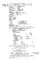
- Fig. 3 is a diagram indicating an example of a logical description language for inputting logical information into the cell generator
- Fig. 4 is a diagram indicating an example of a layout pattern generated in accordance with the logical information of the logical circuit or the logical description language.
- a functional block e.g., a cell in a cell library of a standard cell LSI is, for example, formed by the cell generator by using logical information indicated in a logical circuit diagram as shown in Fig. 2 or a logical description language as shown in Fig. 3.
- the logical circuit diagram as shown in Fig. 2 is, for example, entered into a CAD tool and data of the logical circuit diagram is translated into the logical description language as shown in Fig. 3.
- a layout pattern of the cell is formed by the cell generator by inputting logical information of a logical description language.
- the logical information of the logical description language may be generated not only by the CAD tool by translating the data of the logical circuit diagram, but also directly produced or input by a human operator.
- the layout pattern shown in Fig. 4 is automatically formed by carrying out the placement process and the routing process at the transistor-constitution level.
- the obtained layout pattern of the cell which is output data of the cell generator, is not only of one type but a plurality of types, since plural types of layout patterns can be formed by the cell generator.
- a space occupied by one layout pattern is not the same as that of another layout pattern, and it is difficult to obtain an optimum layout pattern from those plural layout patterns.
- almost all layout patterns formed by the cell generator are larger in size than a layout pattern formed by a person. Consequently, in practice, placement processing of small blocks is previously carried out manually, and only the routing process is carried out by a computer system, e.g., a cell generator.
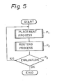
- Figure 5 is a flowchart indicating processes of a program for the cell generator of the prior proposal, and references P1, P2, and P3 denote steps in the flow.
- a placement process is carried out for positioning a transistor at a suitable point.
- a routing process for connection between the terminals of the transistors is carried out.
- the layout pattern is not formed in practice by a placement process at a transistor-constitution level by the cell generator, but is formed by defining functional blocks as shown in Fig. 2 and carrying out a routing process between the defined blocks.
- the routing process has several variations, for example, the wiring configuration can be modified by changing a sequence in the routing process. Therefore, the routing process is carried out including various factors of the wiring sequence and the like.
- the formed layout pattern of the cell (functional block) in the cell generator is evaluated.
- the process is completed.
- the step P3 when wiring portions of the layout pattern formed by the cell generator are not satisfactorily wired (NG), the step P1 is returned to improve the wiring portions so that they are wired in a more orderly manner. Therefore, in order to obtain an optimum cell layout, the above processes should be repeatedly carried out to feed-back information for improvement (for example, tens of thousands times or hundreds of thousands times).
- the layout pattern of a cell formed by a person is much better than that of a cell formed by a computer system, even if the above processes are carried out many times in the computer system.
- targets of the cell generator can be roughly divided into the following two cases.
- a cell generator is equally used for the above two cases in accordance with the flow of processes shown in Fig. 5 without dividing the two cases, and thus the processing time of the cell generator is too long.
- the cell generator does not need to carry out all of the processes, however, in case (I), the cell generator should completely carry out all of the processes of the flow from the beginning.
- the cell generator need only carry out some of the processes shown in Fig. 5.
- the cell generator is equally used for the above two cases (I) and (II), the processes in the cell generator become extensive and the operation speed of the cell generator becomes too slow, and thus, in practice the layout pattern of the cell is mainly formed by a person.
- the present invention provides a method for forming a layout pattern of a semiconductor integrated circuit comprising, a step for analyzing a logical information down to a transistor-constitution level and inputting the analyzed logical information into a cell generator, and a step for automatically forming a layout pattern by a placement process and a routing process at the transistor-constitution level by the cell generator, which steps are the same as in the prior-proposed method.
- the method of the present invention comprises a step of automatically reforming a layout pattern by carrying out only the routing process, when required logical information is the same as existing logical information and a required layout pattern is also the same as an existing layout pattern at the transistor-constitution level, by inputting connection information and layout information of the existing layout pattern into the cell generator, or a step of automatically reforming a layout pattern without analyzing the logical information down to the transistor-constitution level, when required logical information is the same as existing logical information but a required layout pattern is not the same as an existing layout pattern at the transistor-constitution level, by inputting a connection information of the existing layout pattern into the cell generator.
- the required logical information, and thus the existing layout pattern, which is previously formed and used can be utilized for reforming.
- logical information extracted from the existing layout pattern which is existing logical information comprising connection information and layout information
- the cell generator when the required layout pattern has the same configuration as the existing layout pattern, the connection information and the layout information of the existing layout pattern are input into the cell generator, and only a routing process is carried out by the cell generator and the placement process can be deleted in the cell generator.
- the transistor-constitution of the required layout pattern is not the same as that of the existing layout pattern, the logical information of the existing layout pattern is input into the cell generator, the inputting process of the logical information including the logical information can be deleted.
- the placement process and the routing process should be carried out by the cell generator. Consequently, processes in the cell generator become simple and processing time in the cell generator becomes short.
- Figures 6A to 6D are diagrams indicating various transistor-constitutions in half of a basic cell
- Fig. 6E is a circuit diagram of the transistor-constitutions shown in Figs. 6A to 6D
- Fig. 6F is diagram indicating transistor-constitutions in half of a basic cell which has a different transistor-constitution from that shown in Figs. 6A to 6D
- Fig. 6G is a circuit diagram of the transistor-constitution shown in Figs. 6F
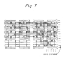
- Fig. 7 is a diagram indicating a variation of the layout pattern shown in Fig. 4.
- a cell generator applied to the present invention automatically reforms the required layout pattern by only a routing process, by inputting connection information and layout information of the existing layout pattern into the cell generator. Namely, an analyzing process of analyzing the logical information down to the transistor-constitution level and a placement process can be deleted.
- a case in which required logical information is the same as existing logical information and a required layout pattern is also the same as an existing layout pattern at the transistor-constitution level is, for example, a case of varying the form of a basic cell shown in Fig. 6A to each of the basic cell shown in Figs. 6B to 6D. Namely, patterns of the transistors Q1,Q2,Q3,Q4 in each basic cell shown in Figs. 6B to 6D are different from that of the transistors Q1,Q2,Q3,Q4 in the basic cell shown in Fig. 6A.
- each transistor Q1,Q2,Q3,Q4 of the basic cell shown in Fig. 6B is longer than that of the basic cell shown in Fig. 6A.
- the gate width of each transistor Q1,Q2,Q3,Q4 of the basic cell shown in Fig. 6C is different from that of the basic cell shown in Fig. 6A
- a shape of the gate electrode of each transistor Q1,Q2,Q3,Q4 of the basic cell shown in Fig. 6D is different from that of the basic cell shown in Figure 6A.
- the basic cells shown in Figs. 6A to 6D are indicated by the same circuit diagram in the transistor-constitution shown in Fig. 6E.
- required logical information is the same as existing logical information and a required layout pattern is also the same as an existing layout pattern in the transistor-constitution level is, for example, a case of varying from a grid distance (which indicates a minimum distance between neighboring wirings) of a layout pattern shown in Fig. 4 to that of a layout pattern in Fig. 7.
- a cell generator applied to the present invention automatically reforms the required layout pattern without analyzing the logical information down to the transistor-constitution level. Namely, an analyzing process of analyzing the logical information down to the transistor-constitution level need not be carried out.
- a case that required logical information is the same as existing logical information but a required layout pattern is not the same as an existing layout pattern in the transistor-constitution level is, for example, a case of varying from a basic cell shown in Fig. 6A to a basic cell shown in Fig. 6F.
- the constitution of the transistor in the basic cell shown in Fig. 6F is different from that of the basic cell shown in Fig. 6A, because source or drain terminals of the transistors Q11,Q12 and the transistors Q13,Q14 are formed by dividing the same electrodes 213a,213b and 217a,217b, however, the source or drain terminals of the transistors Q1,Q2 and the transistors Q3,Q4 are formed by the same electrodes 203 and 207.
- the basic cell shown in Fig. 6F is not indicated by the circuit diagram shown in Fig. 6E, but by the circuit diagram shown in Fig. 6F.
- a required layout pattern is automatically reformed by only a routing process by inputting connection information and layout information of an existing layout pattern into a cell generator.
- a required layout pattern is automatically reformed without analyzing logical information down to the transistor-constitution level by inputting connection information of an existing layout pattern into a cell generator.
- a required layout pattern is easily produced by using an existing layout pattern, even if the size or shape between the required layout pattern and the existing layout pattern are not the same and only the positional relationship of channel regions in the transistors between the required layout pattern and the existing layout pattern are the same.
- the existing layout pattern is constituted by a basic cell.
- an existing layout pattern is almost always formed by a person, this formed layout pattern being nearly an optimum layout pattern, and the formed layout pattern can be used as is when a fixed wiring is changed without changing the size and shape of a transistor.
- a placement process can be deleted from the processes in the flowchart shown in Fig. 5, and thus, processing time can be greatly reduced by deleting a feed-back process and the number of non-connection portions can be held to a minimum by using the existing layout pattern which was practically used.
- a transistor-constitution of a required layout pattern is not the same as that of the existing layout pattern whose logical information is used as input data of the cell generator, the above layout information cannot be used, but the connection information can be used.
- the processes in Fig. 5 are necessary for the cell generator, but a process of inputting a logical circuit diagram and a process of forming a logical description language, which are shown in Figs. 2 and 3, are not necessary, and thus a CAD system using the present invention can be made more efficient.
- an optimum layout is known, (for example, an optimum layout can be known by experience by a designer and the like), the feed-back process of the flowchart in Fig. 5 can be deleted.
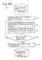
- Figure 8A is a flowchart indicating processes of a program for a cell generator according to the present invention
- Fig. 8B is a flowchart for indicating processes in an extracting process shown in Fig. 8A
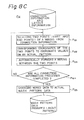
- Fig. 8C is a flowchart for indicating processes in an automatic routing process shown in Fig. 8A.
- references P11 and P12 denote each step of the flow.
- existing layout data which corresponds to mask pattern data of an existing layout pattern is processed in a cell generator, and the flow proceeds to the step P11.
- a step P111 the mask pattern data for graphic data processing is changed, and next a step P112, extracting a transistor by checking for overlapping of graphics between layers by using the changed data, is carried out.
- a step P113 a connection between transistors is recognized by tracing a wire, and then moving to a step P114, for deciding whether processes regarding all data are completed.
- the flow proceeds to a step P115 for changing data for a cell generator, and connection and layout information are obtained.
- connection information and the layout information which correspond to logic information of the existing layout pattern analyzed down to a transistor-constitution level, are stored in a file. Further, the connection information and the layout information of the existing layout pattern (the extracted circuit) are derived in accordance with a verifying method aplied to the existing circuit extraction method. Namely, as shown in Figs. 6A to 6E, connection information at a transistor-constitution level can be extracted by a transistor pattern and a wiring pattern, and the connection information at the transistor-constitution level only indicates connections between terminals of the transistors.
- a step P121 two points are selected, which are a start and an end point, of a wiring in the connection information obtained by the step P11, and next in a step P122, coordinates of the two points are transformed to coordinate values on an actual pattern.
- a step P123 wiring between the two points is automatically carried out
- a step P124 it is decided whether processes regarding all connection information are completed.
- the flow proceeds to a step P 125 for changing wired data to an actual or a required mask pattern data, i.e., required pattern data.
- the step P124 when it is decided that the processes for all connection information are not completed, the flow returns to the step P121.
- the mask pattern data obtained by the step P12 corresponds to layout data of the required layout pattern.
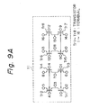
- Figure 9a is a diagram indicating a transistor-constitution in an example of a basic cell
- Fig. 9B is a diagram indicating transistor connections in the basic cell shown in Fig. 9A
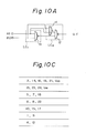
- Fig. 10A is a diagram indicating an example of a logical circuit
- Fig. 10B is a diagram indicating a transistor-constitution in the logical circuit shown in Fig. 10A
- Fig. 10C is a diagram for indicating terminal connections in the logical circuit shown in Fig. 10A.
- reference numeral 11 denotes a basic cell including eight transistors, that is, the basic cell is constituted by P-channel type transistors Tr1, Tr2, Tr7 and Tr8, and N-channel type transistors Tr3, Tr4, Tr5 and Tr6.
- the basic cell shown in Fig. 9A is formed by connecting two blocks each having four transistors indicated in Figs. 6A to 6D, and a semiconductor integrated circuit is constituted by using a plurality of basic cells.
- the basic cell is formed only by transistor patterns, and a logical circuit shown in Fig. 10A is formed by carrying out a routing process as shown in Fig. 10B.
- reference mark ⁇ denotes a terminal of a transistor and each reference numeral close to the mark ⁇ denotes a terminal number of the respective transistor.
- Figure 9B is a list of transistors extracted by the transistor configuration in Fig. 9A.
- references G and S/D denote a gate terminal and a source/drain terminal in each transistor, and the same connection portions are indicated by the same reference numerals.
- a terminal number 3 is commonly connected to source/drain terminals of transistors Tr1 and Tr2, and thus, in the list shown in Fig. 9B, a numeral "3" is shown at portions crossing between one source drain terminal S/D and the transistor Tr2 and the other source drain terminal S/D and the transistor Tr1. Consequently, it can be understood from the list shown in Fig.
- a gate of the transistor Tr1 is commonly connected to a gate of the transistor Tr3, and thus, in the list shown in Fig. 9B, a numeral "3" is shown at portions crossing between a gate terminal G and the transistor Tr1 and the gate terminal G and the transistor Tr3, respectively. Consequently, a logical circuit diagram constituted by transistors of a plurality of basic cells, as indicated in Fig. 9A, can be described by referring to a list of transistor connections as shown in Fig. 9B.
- logical information of an existing layout pattern corresponds, for example, to the data indicated in the list shown in Fig. 9B, and this logical information is input to the cell generator. Further, when the size of transistors in a basic cell or the shape of the transistors and a configuration of the transistor-configuration in the memory cell are not changed, the logical circuit diagram and the list of transistor connections can be used and connection information of the existing layout pattern is input into the cell generator.
- step P11 cince the extracting process in the above step P11 is generally carried out for the purpose of verifying a pattern formed by a person, in a normal case (most cases at the present time), the formed pattern is processed by using circuit extracting program and a circuit shown in figs. 9A or 10B is extracted. Consequently, a new special device is not necessary when extracting connection information and layout information from existing layout data.
- FIG. 10A is a logical circuit diagram including two NAND gates 12 and 13, and OR gate 14.
- Figure 10B is a diagram of transistor connections constituted by a block LC2 including the NAND gate 12 and the OR gate 14, and a block LC1 including the NAND gate 13 on two basic cells 101 and 102.
- Fig. 10A is a logical circuit diagram including two NAND gates 12 and 13, and OR gate 14.
- Figure 10B is a diagram of transistor connections constituted by a block LC2 including the NAND gate 12 and the OR gate 14, and a block LC1 including the NAND gate 13 on two basic cells 101 and 102.
- the basic cell 101 is constituted by P-channel type transistors 111, 112, 117, and 118, and N-channel type transistors 113, 114, 115, and 116
- the basic cell 102 is constituted by P-channel type transistors 121, 122, 127 and 128, and N-channel type transistors 123, 124, 125 and 126.
- reference marks ⁇ and ⁇ denote terminals of the transistors in the basic cells 101 and 102, and each of reference numerals 1 to 32 close to the marks ⁇ and ⁇ denotes a terminal number of the respective transistor.
- terminals connected to power supplies V DD and Vss are shown by the mark ⁇ , and an actual wiring line is shown by a thick solid line.
- transistors 125 to 128 of the basic cell 102 are not used for the logical circuit diagram shown in Fig. 10A.
- the list shown in Fig. 10C indicates connection information of the logical information in a logical circuit having the transistor-constitution shown in Fig. 10B. This connection information indicates connection data between terminals of the transistors.
- information obtained by extracting a circuit from a layout pattern only indicates connection information between the terminals of specific numbers in the transistors. Concretely, in Fig.
- the list indicates that terminals 2, 14, 16, 19, and 21 are connected to the power supply V DD , and terminals 5, 7, and 18 are commonly connected.
- the extracted information is only connection information of terminals in the transistors shown in Fig. 10C.
- the connection information of the terminals is obtained, only a connecting process need be carried out. Consequently, the connection information of the terminals is input to the cell generator, a layout of the transistors is not necessary, and a layout pattern of the cell can be automatically formed by only a routing process in the cell generator.
- connection information and layout information of the existing layout pattern are input into a cell generator, and only a routing process is carried out by the cell generator and a placement process can be deleted in the cell generator.
- a routing process is carried out by the cell generator and a placement process can be deleted in the cell generator.
- logical information of the existing layout pattern is input into a cell generator, and an inputting process of the logical information including logical information can be deleted.
- a placement process and a routing process should be carried out by the cell generator. Consequently, processes in the cell generator become simple and, processing time in the cell generator becomes short.
- a layout pattern of a cell is formed in about ten minutes using a CAD system including a prior-proposed cell generator
- the layout pattern of the cell is formed in only about several seconds by means of the invention.
- a cell library for example, including about one hundred cell layout patterns which can be reformed in a few hours by a CAD system using the present invention, would take some months using the existing method.
Landscapes
- Engineering & Computer Science (AREA)
- Computer Hardware Design (AREA)
- Physics & Mathematics (AREA)
- Theoretical Computer Science (AREA)
- Evolutionary Computation (AREA)
- Geometry (AREA)
- General Engineering & Computer Science (AREA)
- General Physics & Mathematics (AREA)
- Design And Manufacture Of Integrated Circuits (AREA)
- Semiconductor Integrated Circuits (AREA)
Applications Claiming Priority (2)
| Application Number | Priority Date | Filing Date | Title |
|---|---|---|---|
| JP281592/88 | 1988-11-08 | ||
| JP63281592A JP2954223B2 (ja) | 1988-11-08 | 1988-11-08 | 半導体装置の製造方法 |
Publications (3)
| Publication Number | Publication Date |
|---|---|
| EP0368625A2 true EP0368625A2 (de) | 1990-05-16 |
| EP0368625A3 EP0368625A3 (de) | 1991-07-03 |
| EP0368625B1 EP0368625B1 (de) | 1995-03-08 |
Family
ID=17641296
Family Applications (1)
| Application Number | Title | Priority Date | Filing Date |
|---|---|---|---|
| EP89311525A Expired - Lifetime EP0368625B1 (de) | 1988-11-08 | 1989-11-07 | Verfahren und Gerät zur Bildung eines Pattern-Layouts einer integrierten Halbleiterschaltung |
Country Status (5)
| Country | Link |
|---|---|
| US (1) | US5247456A (de) |
| EP (1) | EP0368625B1 (de) |
| JP (1) | JP2954223B2 (de) |
| KR (1) | KR930011055B1 (de) |
| DE (1) | DE68921550T2 (de) |
Families Citing this family (20)
| Publication number | Priority date | Publication date | Assignee | Title |
|---|---|---|---|---|
| JPH05198593A (ja) * | 1992-01-22 | 1993-08-06 | Hitachi Ltd | パラメータ抽出方法 |
| JP2757647B2 (ja) * | 1992-01-27 | 1998-05-25 | 日本電気株式会社 | メッキ膜厚均一化方式 |
| US5347465A (en) * | 1992-05-12 | 1994-09-13 | International Business Machines Corporation | Method of integrated circuit chips design |
| JP2824361B2 (ja) * | 1992-06-09 | 1998-11-11 | 三菱電機株式会社 | クロストーク検証装置 |
| JPH0677324A (ja) * | 1992-06-23 | 1994-03-18 | Fujitsu Ltd | 導体部分のレイアウトデータの変換方法及びその装置 |
| US5576969A (en) * | 1993-03-09 | 1996-11-19 | Nec Corporation | IC comprising functional blocks for which a mask pattern is patterned according to connection and placement data |
| US5566080A (en) * | 1993-09-07 | 1996-10-15 | Fujitsu Limited | Method and apparatus for designing semiconductor device |
| US5828580A (en) | 1994-11-08 | 1998-10-27 | Epic Design Technology, Inc. | Connectivity-based approach for extracting parasitic layout in an integrated circuit |
| US5903469A (en) | 1994-11-08 | 1999-05-11 | Synopsys, Inc. | Method of extracting layout parasitics for nets of an integrated circuit using a connectivity-based approach |
| US5610832A (en) * | 1994-11-22 | 1997-03-11 | Mentor Graphics Corporation | Integrated circuit design apparatus with multiple connection modes |
| US5633807A (en) * | 1995-05-01 | 1997-05-27 | Lucent Technologies Inc. | System and method for generating mask layouts |
| US6577992B1 (en) | 1999-05-07 | 2003-06-10 | Nassda Corporation | Transistor level circuit simulator using hierarchical data |
| US6360133B1 (en) * | 1999-06-17 | 2002-03-19 | Advanced Micro Devices, Inc. | Method and apparatus for automatic routing for reentrant process |
| JP3530450B2 (ja) * | 2000-02-18 | 2004-05-24 | Necエレクトロニクス株式会社 | マクロ回路の配線方法、マクロ回路配線装置、及びマクロ回路 |
| JP2002083757A (ja) * | 2000-07-05 | 2002-03-22 | Mitsubishi Electric Corp | レイアウトパターンデータ補正装置、補正方法及び半導体装置の製造方法並びに記録媒体 |
| US6598214B2 (en) * | 2000-12-21 | 2003-07-22 | Texas Instruments Incorporated | Design method and system for providing transistors with varying active region lengths |
| US7448012B1 (en) | 2004-04-21 | 2008-11-04 | Qi-De Qian | Methods and system for improving integrated circuit layout |
| US8563425B2 (en) * | 2009-06-01 | 2013-10-22 | Advanced Micro Devices | Selective local interconnect to gate in a self aligned local interconnect process |
| US8810280B2 (en) * | 2011-10-06 | 2014-08-19 | Oracle International Corporation | Low leakage spare gates for integrated circuits |
| JP2015230696A (ja) * | 2014-06-06 | 2015-12-21 | 富士通株式会社 | 回路画像出力プログラム、情報処理装置、回路画像出力方法 |
Family Cites Families (14)
| Publication number | Priority date | Publication date | Assignee | Title |
|---|---|---|---|---|
| FR2245984B1 (de) * | 1973-09-27 | 1977-03-18 | Ibm | |
| US4613940A (en) * | 1982-11-09 | 1986-09-23 | International Microelectronic Products | Method and structure for use in designing and building electronic systems in integrated circuits |
| US4584653A (en) * | 1983-03-22 | 1986-04-22 | Fujitsu Limited | Method for manufacturing a gate array integrated circuit device |
| US4580228A (en) * | 1983-06-06 | 1986-04-01 | The United States Of America As Represented By The Secretary Of The Army | Automated design program for LSI and VLSI circuits |
| US4630219A (en) * | 1983-11-23 | 1986-12-16 | International Business Machines Corporation | Element placement method |
| JPS60130140A (ja) * | 1983-12-17 | 1985-07-11 | Toshiba Corp | 半導体集積回路装置 |
| JPS60140733A (ja) * | 1983-12-27 | 1985-07-25 | Fujitsu Ltd | 集積回路パタ−ン生成システム |
| US4636965A (en) * | 1984-05-10 | 1987-01-13 | Rca Corporation | Routing method in computer-aided-customization of universal arrays and resulting integrated circuit |
| US4703435A (en) * | 1984-07-16 | 1987-10-27 | International Business Machines Corporation | Logic Synthesizer |
| US4651284A (en) * | 1984-07-27 | 1987-03-17 | Hitachi, Ltd. | Method and system of circuit pattern understanding and layout |
| KR900001976B1 (ko) * | 1984-11-01 | 1990-03-30 | 가부시끼가이샤 히다찌세이사꾸쇼 | 다수 개의 패턴 발생기를 포함하는 패턴 검사 장치 |
| JPS6358854A (ja) * | 1986-08-29 | 1988-03-14 | Nec Corp | 部品配置生成システム |
| US4745084A (en) * | 1986-11-12 | 1988-05-17 | Vlsi Technology, Inc. | Method of making a customized semiconductor integrated device |
| US4829446A (en) * | 1986-12-12 | 1989-05-09 | Caeco, Inc. | Method and apparatus for recording and rearranging representations of objects in a model of a group of objects located using a co-ordinate system |
-
1988
- 1988-11-08 JP JP63281592A patent/JP2954223B2/ja not_active Expired - Fee Related
-
1989
- 1989-11-07 DE DE68921550T patent/DE68921550T2/de not_active Expired - Fee Related
- 1989-11-07 EP EP89311525A patent/EP0368625B1/de not_active Expired - Lifetime
- 1989-11-08 US US07/433,334 patent/US5247456A/en not_active Expired - Lifetime
- 1989-11-08 KR KR1019890016142A patent/KR930011055B1/ko not_active Expired - Fee Related
Also Published As
| Publication number | Publication date |
|---|---|
| DE68921550D1 (de) | 1995-04-13 |
| EP0368625B1 (de) | 1995-03-08 |
| JPH02128446A (ja) | 1990-05-16 |
| US5247456A (en) | 1993-09-21 |
| DE68921550T2 (de) | 1995-07-06 |
| KR930011055B1 (ko) | 1993-11-20 |
| KR900008646A (ko) | 1990-06-03 |
| EP0368625A3 (de) | 1991-07-03 |
| JP2954223B2 (ja) | 1999-09-27 |
Similar Documents
| Publication | Publication Date | Title |
|---|---|---|
| EP0368625B1 (de) | Verfahren und Gerät zur Bildung eines Pattern-Layouts einer integrierten Halbleiterschaltung | |
| US5351197A (en) | Method and apparatus for designing the layout of a subcircuit in an integrated circuit | |
| US5764533A (en) | Apparatus and methods for generating cell layouts | |
| US5920486A (en) | Parameterized cells for generating dense layouts of VLSI circuits | |
| DE60116769T2 (de) | Verfahren und system zur hierarchischen metallenden-, einschliessungs- und belichtungsprüfung | |
| US6295627B1 (en) | Method and apparatus for the automated design of memory devices | |
| EP0350353B1 (de) | Verarbeitungsverfahren von Layoutdaten | |
| US7159202B2 (en) | Methods, apparatus and computer program products for generating selective netlists that include interconnection influences at pre-layout and post-layout design stages | |
| Hon et al. | A guide to LSI implementation | |
| US11334705B2 (en) | Electrical circuit design using cells with metal lines | |
| US6077308A (en) | Creating layout for integrated circuit structures | |
| US6769107B1 (en) | Method and system for implementing incremental change to circuit design | |
| US5629877A (en) | Process and device composite simulation system and simulation method | |
| US6820048B1 (en) | 4 point derating scheme for propagation delay and setup/hold time computation | |
| Lengauer et al. | The HILL system: a design environment for the hierarchical specification, compaction, and simulation of integrated circuit layouts | |
| US4783749A (en) | Basic cell realized in the CMOS technique and a method for the automatic generation of such a basic cell | |
| US6470477B1 (en) | Methods for converting features to a uniform micron technology in an integrated circuit design and apparatus for doing the same | |
| US9293450B2 (en) | Synthesis of complex cells | |
| US6357035B1 (en) | Method and apparatus for the automated generation of programmable interconnect matrices | |
| US6957406B1 (en) | Analytical placement methods with minimum preplaced components | |
| US7546562B1 (en) | Physical integrated circuit design with uncertain design conditions | |
| Beyls et al. | A design methodology based upon symbolic layout and integrated CAD tools | |
| JP3247455B2 (ja) | 集積回路マスクパターンの検証装置 | |
| JP2001053154A (ja) | セルの作成方法、レイアウト方法、レイアウト装置、記録媒体 | |
| JP3247454B2 (ja) | 集積回路マスクパターンの検証装置 |
Legal Events
| Date | Code | Title | Description |
|---|---|---|---|
| PUAI | Public reference made under article 153(3) epc to a published international application that has entered the european phase |
Free format text: ORIGINAL CODE: 0009012 |
|
| AK | Designated contracting states |
Kind code of ref document: A2 Designated state(s): DE FR GB |
|
| PUAL | Search report despatched |
Free format text: ORIGINAL CODE: 0009013 |
|
| AK | Designated contracting states |
Kind code of ref document: A3 Designated state(s): DE FR GB |
|
| 17P | Request for examination filed |
Effective date: 19910814 |
|
| 17Q | First examination report despatched |
Effective date: 19931015 |
|
| GRAA | (expected) grant |
Free format text: ORIGINAL CODE: 0009210 |
|
| AK | Designated contracting states |
Kind code of ref document: B1 Designated state(s): DE FR GB |
|
| REF | Corresponds to: |
Ref document number: 68921550 Country of ref document: DE Date of ref document: 19950413 |
|
| ET | Fr: translation filed | ||
| PLBE | No opposition filed within time limit |
Free format text: ORIGINAL CODE: 0009261 |
|
| STAA | Information on the status of an ep patent application or granted ep patent |
Free format text: STATUS: NO OPPOSITION FILED WITHIN TIME LIMIT |
|
| 26N | No opposition filed | ||
| REG | Reference to a national code |
Ref country code: GB Ref legal event code: IF02 |
|
| PGFP | Annual fee paid to national office [announced via postgrant information from national office to epo] |
Ref country code: GB Payment date: 20041104 Year of fee payment: 16 Ref country code: DE Payment date: 20041104 Year of fee payment: 16 |
|
| PGFP | Annual fee paid to national office [announced via postgrant information from national office to epo] |
Ref country code: FR Payment date: 20041109 Year of fee payment: 16 |
|
| PG25 | Lapsed in a contracting state [announced via postgrant information from national office to epo] |
Ref country code: GB Free format text: LAPSE BECAUSE OF NON-PAYMENT OF DUE FEES Effective date: 20051107 |
|
| PG25 | Lapsed in a contracting state [announced via postgrant information from national office to epo] |
Ref country code: DE Free format text: LAPSE BECAUSE OF NON-PAYMENT OF DUE FEES Effective date: 20060601 |
|
| GBPC | Gb: european patent ceased through non-payment of renewal fee |
Effective date: 20051107 |
|
| PG25 | Lapsed in a contracting state [announced via postgrant information from national office to epo] |
Ref country code: FR Free format text: LAPSE BECAUSE OF NON-PAYMENT OF DUE FEES Effective date: 20060731 |
|
| REG | Reference to a national code |
Ref country code: FR Ref legal event code: ST Effective date: 20060731 |