EP0368740A1 - Gehäuse für integrierte Schaltung hoher Dichte - Google Patents
Gehäuse für integrierte Schaltung hoher Dichte Download PDFInfo
- Publication number
- EP0368740A1 EP0368740A1 EP19890403051 EP89403051A EP0368740A1 EP 0368740 A1 EP0368740 A1 EP 0368740A1 EP 19890403051 EP19890403051 EP 19890403051 EP 89403051 A EP89403051 A EP 89403051A EP 0368740 A1 EP0368740 A1 EP 0368740A1
- Authority
- EP
- European Patent Office
- Prior art keywords
- legs
- supply
- housing
- tab
- integrated circuit
- Prior art date
- Legal status (The legal status is an assumption and is not a legal conclusion. Google has not performed a legal analysis and makes no representation as to the accuracy of the status listed.)
- Granted
Links
Images


Classifications
-
- H—ELECTRICITY
- H10—SEMICONDUCTOR DEVICES; ELECTRIC SOLID-STATE DEVICES NOT OTHERWISE PROVIDED FOR
- H10W—GENERIC PACKAGES, INTERCONNECTIONS, CONNECTORS OR OTHER CONSTRUCTIONAL DETAILS OF DEVICES COVERED BY CLASS H10
- H10W44/00—Electrical arrangements for controlling or matching impedance
- H10W44/501—Inductive arrangements
-
- H—ELECTRICITY
- H10—SEMICONDUCTOR DEVICES; ELECTRIC SOLID-STATE DEVICES NOT OTHERWISE PROVIDED FOR
- H10W—GENERIC PACKAGES, INTERCONNECTIONS, CONNECTORS OR OTHER CONSTRUCTIONAL DETAILS OF DEVICES COVERED BY CLASS H10
- H10W42/00—Arrangements for protection of devices
-
- H—ELECTRICITY
- H10—SEMICONDUCTOR DEVICES; ELECTRIC SOLID-STATE DEVICES NOT OTHERWISE PROVIDED FOR
- H10W—GENERIC PACKAGES, INTERCONNECTIONS, CONNECTORS OR OTHER CONSTRUCTIONAL DETAILS OF DEVICES COVERED BY CLASS H10
- H10W70/00—Package substrates; Interposers; Redistribution layers [RDL]
- H10W70/40—Leadframes
- H10W70/453—Leadframes comprising flexible metallic tapes
-
- H—ELECTRICITY
- H10—SEMICONDUCTOR DEVICES; ELECTRIC SOLID-STATE DEVICES NOT OTHERWISE PROVIDED FOR
- H10W—GENERIC PACKAGES, INTERCONNECTIONS, CONNECTORS OR OTHER CONSTRUCTIONAL DETAILS OF DEVICES COVERED BY CLASS H10
- H10W72/00—Interconnections or connectors in packages
- H10W72/701—Tape-automated bond [TAB] connectors
-
- H—ELECTRICITY
- H10—SEMICONDUCTOR DEVICES; ELECTRIC SOLID-STATE DEVICES NOT OTHERWISE PROVIDED FOR
- H10W—GENERIC PACKAGES, INTERCONNECTIONS, CONNECTORS OR OTHER CONSTRUCTIONAL DETAILS OF DEVICES COVERED BY CLASS H10
- H10W76/00—Containers; Fillings or auxiliary members therefor; Seals
- H10W76/10—Containers or parts thereof
- H10W76/12—Containers or parts thereof characterised by their shape
- H10W76/15—Containers comprising an insulating or insulated base
- H10W76/157—Containers comprising an insulating or insulated base having interconnections parallel to the insulating or insulated base
-
- H—ELECTRICITY
- H05—ELECTRIC TECHNIQUES NOT OTHERWISE PROVIDED FOR
- H05K—PRINTED CIRCUITS; CASINGS OR CONSTRUCTIONAL DETAILS OF ELECTRIC APPARATUS; MANUFACTURE OF ASSEMBLAGES OF ELECTRICAL COMPONENTS
- H05K2201/00—Indexing scheme relating to printed circuits covered by H05K1/00
- H05K2201/10—Details of components or other objects attached to or integrated in a printed circuit board
- H05K2201/10613—Details of electrical connections of non-printed components, e.g. special leads
- H05K2201/10621—Components characterised by their electrical contacts
- H05K2201/10659—Different types of terminals for the same component, e.g. solder balls combined with leads
-
- H—ELECTRICITY
- H05—ELECTRIC TECHNIQUES NOT OTHERWISE PROVIDED FOR
- H05K—PRINTED CIRCUITS; CASINGS OR CONSTRUCTIONAL DETAILS OF ELECTRIC APPARATUS; MANUFACTURE OF ASSEMBLAGES OF ELECTRICAL COMPONENTS
- H05K3/00—Apparatus or processes for manufacturing printed circuits
- H05K3/30—Assembling printed circuits with electric components, e.g. with resistors
- H05K3/32—Assembling printed circuits with electric components, e.g. with resistors electrically connecting electric components or wires to printed circuits
- H05K3/34—Assembling printed circuits with electric components, e.g. with resistors electrically connecting electric components or wires to printed circuits by soldering
- H05K3/341—Surface mounted components
- H05K3/3421—Leaded components
-
- H—ELECTRICITY
- H05—ELECTRIC TECHNIQUES NOT OTHERWISE PROVIDED FOR
- H05K—PRINTED CIRCUITS; CASINGS OR CONSTRUCTIONAL DETAILS OF ELECTRIC APPARATUS; MANUFACTURE OF ASSEMBLAGES OF ELECTRICAL COMPONENTS
- H05K3/00—Apparatus or processes for manufacturing printed circuits
- H05K3/30—Assembling printed circuits with electric components, e.g. with resistors
- H05K3/32—Assembling printed circuits with electric components, e.g. with resistors electrically connecting electric components or wires to printed circuits
- H05K3/34—Assembling printed circuits with electric components, e.g. with resistors electrically connecting electric components or wires to printed circuits by soldering
- H05K3/3447—Lead-in-hole components
Definitions
- the subject of the invention is a high-density integrated circuit package, also called a Very Large Scale Integration chip (VLSI) or chip, an integrated circuit TAB (Tape-Automated Bonding) support, adapted to the package, and a card. interconnection intended to receive such a box.
- VLSI Very Large Scale Integration chip
- TAB Tape-Automated Bonding
- the TAB support of such an integrated circuit comprises an insulating substrate carrying a plurality of radiating lugs, called the TAB spider.
- the substrate is usually made of a flexible plastic material, such as that known under the trademark Kapton, and consists of one or more concentric frames.
- the legs of the support converge towards a central region of the substrate to be connected to the input-output terminals of the integrated circuit according to an operation called ILB (Inner Lead Bonding), usually consisting of thermocompression welding.
- ILB Inner Lead Bonding
- the TAB support of an integrated circuit is usually cut from a film of cinematographic type, called TAB film, comprising a longitudinal succession of TAB spiders and lateral perforations used to move and position the film.
- Supply potentials are mass and usually one or two different predetermined values. During the operation of the integrated circuit, these potentials must remain stable despite the different values of current intensity demanded by the circuits called to operate in the integrated circuit. Therefore, the supply legs constitute as many electric transmission lines having a reactive self-induction component in response to variations in current. The self-induction component of each leg is therefore proportional to its length. On the other hand, the intensity of the supply current is currently high. For example, some integrated circuits can temporarily dissipate up to 6 watts at a voltage of 3 volts, thus requiring the flow of two amps.
- the legs must be narrow and very close to each other.
- the flow of a high intensity of supply current must therefore be made in a plurality of supply tabs.
- the small sections of the legs increase their ohmic resistance.
- the solution currently adopted consists in applying the supply potentials to respective solid terminals, external to the housing and connected inside the latter to respective potential conducting planes.
- the potential planes are associated with discrete decoupling capacitors, incorporated in the housing, or form the plates of a decoupling capacitor. They are also connected to the corresponding supply legs, as close as possible to the integrated circuit. The length of the supply legs is thus reduced approximately to the length separating the supply terminals of the integrated circuit from the neighboring potential planes.
- This solution therefore has the advantage of reducing the ohmic impedance and the reactive self-induction component of the supply circuit in the housing. It results in the fact that only the signal tabs are long and extend over the entire support to be connected to the outside of the housing.
- TAB supports carrying short supply legs and long signal legs poses in practice the problem of interference of signals flowing in neighboring legs. Indeed, two large neighboring legs of signals on a high density TAB support are substantially parallel and very close to one another (from 50 to 100 microns) and constitute two electric lines acting mutually on each other. .
- One solution would be to divide the signal legs into a plurality of groups isolated from each other by conductors with fixed potentials, such as supply conductors.
- the lengthening of the supply legs to constitute electromagnetic shielding elements between two adjacent groups of signal legs would again pose the problem of the reactive self-induction component of these long supply legs.
- the invention provides a solution to this problem, thus offering the advantage of obtaining a reduced self-induction component and effective shielding between signal legs.
- a high-density integrated circuit package comprising external power potential planes parallel to the integrated circuit and a TAB spider provided with long signal legs and a plurality of power legs connected to proximity of the integrated circuit to the inner periphery of the respective potential planes, is characterized in that the supply tabs of at least part of said plurality are also connected to the outer periphery of the respective potential planes and are arranged among the signal tabs to serve as shielding elements between groups of signal tabs.
- An integrated circuit TAB support for the implementation of the previous box comprising a substrate concentric with the integrated circuit, carrying a TAB spider and pierced at its inner periphery under a plurality of spider legs, is characterized in that the substrate is also pierced at its outer periphery under the legs of at least part of said plurality and in that the legs of said part are distributed substantially uniformly among the legs outside said plurality.
- an interconnection card according to the invention for the connection of the previous box, incorporating potential planes and a signal interconnection network and having on one face supply terminals for the connection of the potential of the box and a ring of pads intended for the connection of the spider TAB of the box to the signal interconnection network of the card, characterized in that the ring comprises connection pads connected to said potential planes of the card.
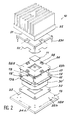
- FIGS. 1 and 2 illustrate the preferred embodiment according to the invention of an integrated circuit housing 10 11 mounted on a TAB support 12.
- the housing 10 shown in Figure 1 is a half view in median and axial section along the axis ZZ ′ passing perpendicular to the integrated circuit 11 at its center. It is also illustrated in its final position of connection with an interconnection card 13, illustrated schematically and partially in the form of a printed circuit board.
- FIGS. 3, 4 and 5 illustrate exemplary embodiments according to the invention of the TAB support 12 included in the housing 10.
- the integrated circuit 11 carries on its active face peripheral input-output terminals 14, generally arranged in a line or in staggered rows.
- the terminals 14 are fixed to the inner ends of respective conductors (lugs) 15 assembled in a bundle (TAB spider) 16 on one face of a flexible electrically insulating substrate 17.
- the substrate 17 illustrated is formed of a single frame for the convenience of the drawings, knowing that in practice it usually consists of several frames concentric with the axis ZZ ′ of the integrated circuit 11.
- the support TAB 12 has been cut from a film TAB 18 along the line L indicated by a ghost line. On a conventional support, only the signal tabs 15s are extended to the film 18 and cut along line L, since the supply tabs are very short, like the tabs 15′a and 15′b illustrated in FIG. 3.
- the supply tabs 15′a, 15′b stop near the integrated circuit 11, at the inner periphery of the frame 17 of the substrate.
- the short legs 15′a, 15′b stop at the level of holes 19 made in the inner periphery of the frame 17, and the long legs 15a, 15b pass through similar holes 19 formed in the inner periphery of the frame 17.
- the support TAB 12 is thus adapted to the embodiment of the housing 10 which will now be described.
- the integrated circuit 11 has its base fixed by a conductive seal 20 to a base 21 made of an electrically and thermally conductive material, such as copper or aluminum.
- the base 21 is a substantially square rigid plate, coaxial with the axis ZZ ′ and provided with a coaxial column for fixing a radiator 22.
- the corners of the base 21 extend along its diagonals to form four arms carrying four supply terminals 23a constituted by conductive piles perpendicular to the base.
- the housing 10 comprises a decoupling device 24 composed of an insulating frame 25 provided on its two faces with two respective conductive planes 26a, 26b in connection with corresponding conductive islands 27a, 27b as well as with four capacitors 28.
- the device decoupling 24 coaxially surrounds the integrated circuit 11.
- the conducting plane 26a is fixed to the base 21 by the seal 20 duly extended.
- the conductive plane 26b is in connection with four supply terminals 23b formed of piles fixed to the four sides of the frame 25.
- against the conductive plane 26b is supported the substrate 17 of the TAB support 12.
- the islands 27a , 27b are arranged at the inner periphery of the frame 25, in correspondence with the holes 19 in the substrate 17 so as to be in contact with the respective feed legs 15a, 15b, 15′a, 15′b of the spider TAB 16
- the islands 27b are extensions of the conducting plane 26b and the islets 27a are connected to the conducting plane 26a by means of pillars 29a passing through the frame 25.
- the housing 10 is closed by a cover 30, advantageously made of a conductive material and fixed mechanically and electrically to the piles 23b, while being isolated from the spider 16 by a seal 30 ′.
- the interconnection card 13 on which the housing 10 is applied consists of two conducting planes 31a, 31b placed respectively at the supply potentials Ua and Ub, of metallized holes 32a, 32b in respective connection with the conducting planes 31a, 31b and with the supply piles 23a, 23b of the housing 10, and of a signal interconnection network 33 formed of conductive layers such as the two layers illustrated by a solid line in FIG. 1 and of connection pads 34s aligned along a ring 35 concentric with the axis ZZ ′ and placed in correspondence with the outer ends of the signal tabs 15s of the spider TAB 16 of the housing 10.
- the connection pads 34s are connected to the signal interconnection network 33 by conductive pillars 33, illustrated by a dashed line in FIG. 1.
- At least part of the set of feed legs of the spider TAB 16 is made of long feed legs 15a, 15b connected at the same time to the inner peripheral islands 27a, 27b of the decoupling device 24 of the housing 10 and on external peripheral islands 27′a, 27′b of the decoupling device 24.
- the TAB support 12 illustrated in FIG. 3 and mounted in the housing 10 of FIG. 1 tabs short supply 15a, 15b remain, and the long supply lugs 15a, 15b come at the level of holes 19 ′ formed in the external periphery of the substrate 17 of the TAB support 12.
- the external peripheral islands 27′b are extensions of the potential plane 26b and the islands 27′a are connected to the potential plane 26a by respective pillars 29′a passing through the frame 25.
- the connection of the supply tabs in the holes 19, 19 ′ is preferably made p ar tin-lead soldering on the corresponding islands 27a, 27′a, 27b, 27′b raised relative to the conducting plane 26b.
- FIG 4 is a partial sectional view of enlarged detail of the film 18 shown in Figure 3, used for the manufacture of the housing shown in Figure 1.
- the supply tabs 15a, 15b are extended in the same way as the signal tabs 15s of the spider TAB 16.
- the outer ends of the spider TAB 16 of the housing 10 are connected to corresponding pads 34a, 34b of the card 13.
- the pads 34a , 34b are distributed among the signal ranges 34s in the crown 35.
- the ranges 34a, 34b are connected to the respective potential planes 31a, 31b by means of conductive pillars 36.
- the elongated supply tabs 15a, 15b are arranged among the signal tabs 15s to serve as electromagnetic shielding elements between groups of signal tabs.
- an elongated supply conductor 15a or 15b separates two adjacent groups of signal tabs.
- the groups illustrated consist only of two signal tabs. In practice, each group obviously consists of a larger number of signal legs 15s, this number being able to vary slightly between adjacent groups.
- the elongation of the supply legs 15a, 15b in a TAB spider 16 and their connection to the inner and outer periphery of the conducting planes 26a, 26b surrounding the integrated circuit 11 solves the problem of electromagnetic shielding between groups of legs 15s signals.
- a long single supply leg 15a or 15b has greater self-induction.
- the total self-induction of all the long supply legs 15a, 15b has the value of the self-induction of a long leg shunted according to the invention, divided by the total number of long legs. It finally follows that the total self-induction of the supply circuit in a housing 10 according to the invention is substantially equal to that of a conventional housing.
- the embodiment illustrated in Figures 1, 2, 3, 4 and 6 can receive various variants according to the invention.
- the short feed legs 15′a, 15′b in the spider 16 shown in FIG. 3 can be eliminated so that all of the feed legs are extended to serve as shielding elements between groups of signal tabs 15s.
- the extension of the supply tabs can be limited to their peripheral connection outside the islands 27′a, 27′b with the conducting planes 26a, 26b of the housing 10.
- This variant is shown in Figure 5.
- the variants can coexist in the same spider.
- the production of the housing 10 illustrated in FIGS. 1 and 2 requires the drilling of holes 19 and 19 ′ in the substrate 17 of the TAB support 12 for the connection of the supply tabs with the respective conducting planes of the decoupling device in The box.
- the TAB spider 16 could be applied directly against this face, with the substrate 17 placed towards the cover 30. Consequently, the connection of the islands with the corresponding long supply legs could be made directly without requiring the drilling of the holes in the substrate 17.
- a set of holes 19 or 19 ′ can be substituted for a slot, formed for example in each side of the substrate 17.
- all of the holes 19 or 19 ′ could be formed by the space of two adjacent frames dividing the substrate 17. The drilling of holes under the feed tabs is therefore an expression which includes these extensions. For these extensions, the holes then extend under the signal tabs.
Landscapes
- Lead Frames For Integrated Circuits (AREA)
- Wire Bonding (AREA)
- Semiconductor Integrated Circuits (AREA)
- Coupling Device And Connection With Printed Circuit (AREA)
Applications Claiming Priority (2)
| Application Number | Priority Date | Filing Date | Title |
|---|---|---|---|
| FR8814542A FR2638896B1 (fr) | 1988-11-08 | 1988-11-08 | Boitier de circuit integre de haute densite, support de circuit integre et carte d'interconnexion en resultant |
| FR8814542 | 1988-11-08 |
Publications (2)
| Publication Number | Publication Date |
|---|---|
| EP0368740A1 true EP0368740A1 (de) | 1990-05-16 |
| EP0368740B1 EP0368740B1 (de) | 1995-02-15 |
Family
ID=9371659
Family Applications (1)
| Application Number | Title | Priority Date | Filing Date |
|---|---|---|---|
| EP89403051A Expired - Lifetime EP0368740B1 (de) | 1988-11-08 | 1989-11-07 | Gehäuse für integrierte Schaltung hoher Dichte |
Country Status (5)
| Country | Link |
|---|---|
| EP (1) | EP0368740B1 (de) |
| JP (1) | JPH0618225B2 (de) |
| DE (1) | DE68921148T2 (de) |
| ES (1) | ES2070923T3 (de) |
| FR (1) | FR2638896B1 (de) |
Cited By (2)
| Publication number | Priority date | Publication date | Assignee | Title |
|---|---|---|---|---|
| EP0678917A1 (de) * | 1994-04-22 | 1995-10-25 | Nec Corporation | Trägerelement für Kühlvorrichtung und elektronisches Gehäuse mit einem solchen Element |
| EP0800211A1 (de) * | 1996-04-03 | 1997-10-08 | Bull S.A. | Integriertes Schaltungsgehäuse |
Families Citing this family (1)
| Publication number | Priority date | Publication date | Assignee | Title |
|---|---|---|---|---|
| JP2904123B2 (ja) * | 1996-05-10 | 1999-06-14 | 日本電気株式会社 | 多層フィルムキャリアの製造方法 |
Citations (5)
| Publication number | Priority date | Publication date | Assignee | Title |
|---|---|---|---|---|
| EP0214307A1 (de) * | 1985-02-28 | 1987-03-18 | Sony Corporation | Halbleiterschaltungsanordnung |
| US4680613A (en) * | 1983-12-01 | 1987-07-14 | Fairchild Semiconductor Corporation | Low impedance package for integrated circuit die |
| DE3706251A1 (de) * | 1986-02-28 | 1987-09-03 | Canon Kk | Halbleitervorrichtung |
| EP0239494A1 (de) * | 1986-03-28 | 1987-09-30 | Bull S.A. | Gehäuse für integrierte Schaltung |
| EP0285277A1 (de) * | 1987-03-31 | 1988-10-05 | Amp Incorporated | Chipträger mit Mitteln für Energiespeicherung |
Family Cites Families (1)
| Publication number | Priority date | Publication date | Assignee | Title |
|---|---|---|---|---|
| EP0282617A1 (de) * | 1987-03-18 | 1988-09-21 | Texas Instruments Deutschland Gmbh | Integrierte Schaltung mit einer elektrisch leitenden Trägerplatte |
-
1988
- 1988-11-08 FR FR8814542A patent/FR2638896B1/fr not_active Expired - Lifetime
-
1989
- 1989-11-07 EP EP89403051A patent/EP0368740B1/de not_active Expired - Lifetime
- 1989-11-07 ES ES89403051T patent/ES2070923T3/es not_active Expired - Lifetime
- 1989-11-07 DE DE68921148T patent/DE68921148T2/de not_active Expired - Fee Related
- 1989-11-08 JP JP1290948A patent/JPH0618225B2/ja not_active Expired - Fee Related
Patent Citations (5)
| Publication number | Priority date | Publication date | Assignee | Title |
|---|---|---|---|---|
| US4680613A (en) * | 1983-12-01 | 1987-07-14 | Fairchild Semiconductor Corporation | Low impedance package for integrated circuit die |
| EP0214307A1 (de) * | 1985-02-28 | 1987-03-18 | Sony Corporation | Halbleiterschaltungsanordnung |
| DE3706251A1 (de) * | 1986-02-28 | 1987-09-03 | Canon Kk | Halbleitervorrichtung |
| EP0239494A1 (de) * | 1986-03-28 | 1987-09-30 | Bull S.A. | Gehäuse für integrierte Schaltung |
| EP0285277A1 (de) * | 1987-03-31 | 1988-10-05 | Amp Incorporated | Chipträger mit Mitteln für Energiespeicherung |
Non-Patent Citations (1)
| Title |
|---|
| IBM TECHNICAL DISCLOSURE BULLETIN, vol. 21, no. 5, octobre 1978, pages 1895-1897, New York, US; S. MAGDO: "Low inductance module" * |
Cited By (4)
| Publication number | Priority date | Publication date | Assignee | Title |
|---|---|---|---|---|
| EP0678917A1 (de) * | 1994-04-22 | 1995-10-25 | Nec Corporation | Trägerelement für Kühlvorrichtung und elektronisches Gehäuse mit einem solchen Element |
| EP0800211A1 (de) * | 1996-04-03 | 1997-10-08 | Bull S.A. | Integriertes Schaltungsgehäuse |
| FR2747235A1 (fr) * | 1996-04-03 | 1997-10-10 | Bull Sa | Boitier de circuit integre |
| US5925925A (en) * | 1996-04-03 | 1999-07-20 | Bull, S.A. | Three-dimensional integrated circuit package having conductors at different fixed potentials |
Also Published As
| Publication number | Publication date |
|---|---|
| DE68921148D1 (de) | 1995-03-23 |
| FR2638896A1 (fr) | 1990-05-11 |
| ES2070923T3 (es) | 1995-06-16 |
| JPH02183548A (ja) | 1990-07-18 |
| DE68921148T2 (de) | 1995-06-14 |
| JPH0618225B2 (ja) | 1994-03-09 |
| EP0368740B1 (de) | 1995-02-15 |
| FR2638896B1 (fr) | 1990-12-21 |
Similar Documents
| Publication | Publication Date | Title |
|---|---|---|
| EP0133125B1 (de) | Gehäuse für einen elektronischen Baustein mit einem Kondensator | |
| FR2621173A1 (fr) | Boitier pour circuit integre de haute densite | |
| EP0239494B1 (de) | Gehäuse für integrierte Schaltung | |
| FR2700416A1 (fr) | Dispositif à semiconducteurs comportant un élément semiconducteur sur un élément de montage. | |
| EP0228953B1 (de) | Verkapselungsgehäuse für eine elektronische Schaltung | |
| FR2735648A1 (fr) | Procede de refroidissement d'un circuit integre monte dans un boitier | |
| US5254871A (en) | Very large scale integrated circuit package, integrated circuit carrier and resultant interconnection board | |
| FR2747235A1 (fr) | Boitier de circuit integre | |
| EP0368740B1 (de) | Gehäuse für integrierte Schaltung hoher Dichte | |
| FR2495834A1 (fr) | Dispositif a circuits integres de haute densite | |
| FR2638895A1 (fr) | Support de circuit integre et son procede de fabrication, circuit integre adapte au support et boitier en resultant | |
| EP0161166B1 (de) | Kompakter Addierer mit Halbleiteranordnungen im Hyperfrequenz-Betrieb | |
| FR2693031A1 (fr) | Dispositif à semiconducteurs, substrat et cadre de montage pour ce dispositif. | |
| EP0179714B1 (de) | Verfahren zur Montierung zweier Halbleiterbauelemente in einem gemeinsamen Gehäuse und gemäss diesem Verfahren hergestellte Anordnung | |
| FR2629271A1 (fr) | Dispositif d'interconnexion et de protection d'une pastille nue de composant hyperfrequence | |
| EP1252804B1 (de) | Makrobauteilgeformtes kommunikationsendgerät, zwischenstück, und vorrichtung zur verbindung mit einer grundplatine | |
| FR2503933A1 (fr) | Circuit integre comprenant un reseau de transistors | |
| FR2583251A1 (fr) | Ensemble electronique composite et procede pour ameliorer l'amortissement de l'alimentation d'un circuit integre | |
| EP0030168B1 (de) | Vorrichtung zur Parallelschaltung von Höchstfrequenz-Leistungstransistoren | |
| FR2620275A1 (fr) | Boitier pour le montage en surface d'un composant fonctionnant en hyperfrequences | |
| FR2564244A1 (fr) | Structure de montage pour circuits integres rapides | |
| FR2536910A1 (fr) | Transistor a effet de champ a double grille de haute puissance | |
| CA1094213A (fr) | Ensemble de liaison d'une carte-support de circuit electrique et d'un cadre exterieur | |
| FR2495835A1 (fr) | Dispositif a circuits integres a reseau metallique d'interconnexion, et procede de fabrication de ce dispositif | |
| FR2618255A1 (fr) | Bloc de conditionnement pour le montage et l'interconnexion de puces semiconductrices. |
Legal Events
| Date | Code | Title | Description |
|---|---|---|---|
| PUAI | Public reference made under article 153(3) epc to a published international application that has entered the european phase |
Free format text: ORIGINAL CODE: 0009012 |
|
| AK | Designated contracting states |
Kind code of ref document: A1 Designated state(s): CH DE ES FR GB IT LI NL SE |
|
| 17P | Request for examination filed |
Effective date: 19900605 |
|
| 17Q | First examination report despatched |
Effective date: 19920224 |
|
| RAP3 | Party data changed (applicant data changed or rights of an application transferred) |
Owner name: BULL S.A. |
|
| GRAA | (expected) grant |
Free format text: ORIGINAL CODE: 0009210 |
|
| AK | Designated contracting states |
Kind code of ref document: B1 Designated state(s): CH DE ES FR GB IT LI NL SE |
|
| REF | Corresponds to: |
Ref document number: 68921148 Country of ref document: DE Date of ref document: 19950323 |
|
| GBT | Gb: translation of ep patent filed (gb section 77(6)(a)/1977) |
Effective date: 19950308 |
|
| ITF | It: translation for a ep patent filed | ||
| REG | Reference to a national code |
Ref country code: ES Ref legal event code: FG2A Ref document number: 2070923 Country of ref document: ES Kind code of ref document: T3 |
|
| PLBE | No opposition filed within time limit |
Free format text: ORIGINAL CODE: 0009261 |
|
| STAA | Information on the status of an ep patent application or granted ep patent |
Free format text: STATUS: NO OPPOSITION FILED WITHIN TIME LIMIT |
|
| 26N | No opposition filed | ||
| REG | Reference to a national code |
Ref country code: GB Ref legal event code: IF02 |
|
| PGFP | Annual fee paid to national office [announced via postgrant information from national office to epo] |
Ref country code: SE Payment date: 20041025 Year of fee payment: 16 |
|
| PGFP | Annual fee paid to national office [announced via postgrant information from national office to epo] |
Ref country code: CH Payment date: 20041026 Year of fee payment: 16 Ref country code: DE Payment date: 20041026 Year of fee payment: 16 Ref country code: GB Payment date: 20041026 Year of fee payment: 16 |
|
| PGFP | Annual fee paid to national office [announced via postgrant information from national office to epo] |
Ref country code: ES Payment date: 20041105 Year of fee payment: 16 |
|
| PG25 | Lapsed in a contracting state [announced via postgrant information from national office to epo] |
Ref country code: IT Free format text: LAPSE BECAUSE OF NON-PAYMENT OF DUE FEES;WARNING: LAPSES OF ITALIAN PATENTS WITH EFFECTIVE DATE BEFORE 2007 MAY HAVE OCCURRED AT ANY TIME BEFORE 2007. THE CORRECT EFFECTIVE DATE MAY BE DIFFERENT FROM THE ONE RECORDED. Effective date: 20051107 Ref country code: GB Free format text: LAPSE BECAUSE OF NON-PAYMENT OF DUE FEES Effective date: 20051107 |
|
| PG25 | Lapsed in a contracting state [announced via postgrant information from national office to epo] |
Ref country code: ES Free format text: LAPSE BECAUSE OF NON-PAYMENT OF DUE FEES Effective date: 20051108 Ref country code: SE Free format text: LAPSE BECAUSE OF NON-PAYMENT OF DUE FEES Effective date: 20051108 |
|
| PG25 | Lapsed in a contracting state [announced via postgrant information from national office to epo] |
Ref country code: CH Free format text: LAPSE BECAUSE OF NON-PAYMENT OF DUE FEES Effective date: 20051130 Ref country code: LI Free format text: LAPSE BECAUSE OF NON-PAYMENT OF DUE FEES Effective date: 20051130 |
|
| PG25 | Lapsed in a contracting state [announced via postgrant information from national office to epo] |
Ref country code: DE Free format text: LAPSE BECAUSE OF NON-PAYMENT OF DUE FEES Effective date: 20060601 |
|
| REG | Reference to a national code |
Ref country code: CH Ref legal event code: PL |
|
| EUG | Se: european patent has lapsed | ||
| GBPC | Gb: european patent ceased through non-payment of renewal fee |
Effective date: 20051107 |
|
| PGFP | Annual fee paid to national office [announced via postgrant information from national office to epo] |
Ref country code: FR Payment date: 20061128 Year of fee payment: 18 |
|
| REG | Reference to a national code |
Ref country code: ES Ref legal event code: FD2A Effective date: 20051108 |
|
| PGFP | Annual fee paid to national office [announced via postgrant information from national office to epo] |
Ref country code: NL Payment date: 20071026 Year of fee payment: 19 |
|
| REG | Reference to a national code |
Ref country code: FR Ref legal event code: ST Effective date: 20080930 |
|
| PG25 | Lapsed in a contracting state [announced via postgrant information from national office to epo] |
Ref country code: FR Free format text: LAPSE BECAUSE OF NON-PAYMENT OF DUE FEES Effective date: 20071130 |
|
| PG25 | Lapsed in a contracting state [announced via postgrant information from national office to epo] |
Ref country code: NL Free format text: LAPSE BECAUSE OF NON-PAYMENT OF DUE FEES Effective date: 20090601 |
|
| NLV4 | Nl: lapsed or anulled due to non-payment of the annual fee |
Effective date: 20090601 |