EP0369449A1 - Socle pour composant semi-conducteur - Google Patents
Socle pour composant semi-conducteur Download PDFInfo
- Publication number
- EP0369449A1 EP0369449A1 EP89121239A EP89121239A EP0369449A1 EP 0369449 A1 EP0369449 A1 EP 0369449A1 EP 89121239 A EP89121239 A EP 89121239A EP 89121239 A EP89121239 A EP 89121239A EP 0369449 A1 EP0369449 A1 EP 0369449A1
- Authority
- EP
- European Patent Office
- Prior art keywords
- posts
- seat
- film
- post
- center point
- Prior art date
- Legal status (The legal status is an assumption and is not a legal conclusion. Google has not performed a legal analysis and makes no representation as to the accuracy of the status listed.)
- Granted
Links
Images

Classifications
-
- H—ELECTRICITY
- H05—ELECTRIC TECHNIQUES NOT OTHERWISE PROVIDED FOR
- H05K—PRINTED CIRCUITS; CASINGS OR CONSTRUCTIONAL DETAILS OF ELECTRIC APPARATUS; MANUFACTURE OF ASSEMBLAGES OF ELECTRICAL COMPONENTS
- H05K7/00—Constructional details common to different types of electric apparatus
- H05K7/02—Arrangements of circuit components or wiring on supporting structure
- H05K7/10—Plug-in assemblages of components, e.g. IC sockets
- H05K7/1053—Plug-in assemblages of components, e.g. IC sockets having interior leads
- H05K7/1061—Plug-in assemblages of components, e.g. IC sockets having interior leads co-operating by abutting
Definitions
- This invention relates to the mounting of a semiconductor device of the tape automated bonded (TAB) type, to a socket for connection to external circuitry, the semiconductor device being bonded, in manufacture, to leads attached to a segment of film.
- TAB tape automated bonded
- semiconductor device means any semiconductor apparatus or device including discreet circuit components or integrated circuits, especially those of higher density.
- the invention concerns the minimization of such mismatch in order to optimize mating registration between the film and the socket.
- United States Patent Number 4,007,479 a fixture for a segment of film strip, in which the film is located between pins or posts projecting from one part of the fixture and which engage in openings in the other part.
- United States Patent Number 4,696,526, a two part carrier for a film mounted semiconductor, in which square posts on one part are sized to fit sprocket holes in the film in order to align it with the carrier.
- United States Reissue Patent Number Re30,604 discloses a reusable fixture for a film mounted semiconductor device having lugs which are positioned to project through sprocket holes in the film and are located so that wedge shaped protrusions of the lugs overlie the film.
- the film carrying means described in the three patent specifications mentioned above are intended for holding the film in position, only temporarily, while certain manufacturing steps are carried out thereupon so that the problem of socketing, for permanent use, a film mounted semiconductor device, and in particular the problems outlined above, with which the present invention is concerned, are accordingly not addressed in these specifications.
- the invention proceed from the realization, that when supported between the protective carrier and the socket, there should be free relative movement between the film, and the carrier and socket to allow for the difference in materials mentioned above in the face of temperature and ambient humidity changes.
- an electrical connector assembly comprises, in combination, a semiconductor device bonded to leads attached to a segment of film, a protective carrier for the film, and an insulating socket mating with the protective carrier and having electrical contact elements for connecting the semiconductor device to an external circuit and for engaging contact pads on the leads of the semiconductor device.
- a peripheral margin of the film segment is formed with a plurality of pairs of slots, each of which is elongate in the direction of a center point of the film, within said margin, the slots of each pair being located on diametrically opposite sides of the center point.
- the protective carrier provides a first seat for the film segment and from which seat upstand a plurality of posts each engaged in a respective one of the elongate slots in the margin of the film segment, with substantial clearance in the longitudinal direction of the slot, but fitting the slot in the transverse direction thereof.
- the socket provides a second seat for the film segment, there being formed in the second seat, a plurality of pockets each snugly receiving a respective one of the posts on the protective carrier.
- the slots in the film segment, the posts on the protective carrier, the pockets in the insulating socket are four in number, according to a preferred embodiment of the invention, each slot of one pair slots being angularly spaced by 90° about the center point of the film segment from each of the slots of the other pair.
- the film segment will normally be substantially square and the slots may be located proximate to the corners of the square or each may be located centrally of one side thereof. Since each post fits its slot in the transverse direction thereof, the center lines of the carrier, the film and the socket are maintained concentric when these parts have been assembled.
- the posts are preferably very thin, having a major dimension, of the order, for example, of .040 inches (about 1mm).
- the posts would in the absence of counter-measures, accordingly tend to break at their roots when the assembly is being put together.
- the root of each post is positioned in a well extending below the surface of the protective carrier and supporting ribs connected to the posts and to the peripheral wall of the well are provided, so that the posts will not break at their roots.
- the well may be circular and the ribs may extend radially thereof, being formed integrally as with the posts and insulating material of the carrier.
- a protective carrier for a semiconductor device bonded to leads attached to a segment of film is in the form of a plate defining a planar seat for the film segment, the seat having a peripheral margin and a center point within the margin.
- Two pairs of posts upstand from the margin, normally of the seat, each post being of elongate cross section in the direction of the center point of the seat.
- the posts of each pair are located on diametrically opposite sides of the center point, each post having a base portion which extends into a well in said margin, the well having a peripheral wall and the root of the post being supported therein by means of opposed ribs which connect the root of the post to the peripheral wall of the well.
- a method of socketing a semiconductor device bonded to leads attached to a segment of film having a peripheral margin and a center point within the margin comprises the steps of; forming in said peripheral margin a plurality of pairs of slots each of which is elongate in the direction of said enter point, the slots of each pair being located on diametrically opposite sides of the center point; threading through each slot, a post upstanding from a protective carrier for the film segment, with play only in the longitudinal direction of the slot; and inserting each post snugly into a respective pocket of a semiconductor device socket so that the film is enclosed between the carrier and the socket.
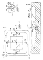
- a protective carrier 4 molded in one piece from insulating material is substantially square as seen in plan view, being in the form of a plate defining a seat 6, which is planar, for a semiconductor device 8 ( Figure 4) mounted on a segment 10 of film and which is described in more detail below.
- the seat 6, which is substantially rectangular, is surrounded by a rim 12 and has a center point C within a peripheral margin 14 of the seat 6.
- each post extends from the base 6 to a position beyond the rim 12 and has a root 20 located in a well 22 extending into the material of the carrier 4 below the surface of the margin 14 of the seat 6.
- the root 20 is formed integrally with the base 24 of the well 22 and is positioned centrally of the circular peripheral wall 26 of well 22. Also formed integrally with the base 24 and with the wall 26 are supporting ribs 28.
- Each post 16 and 18 is of constant elongate rectangular cross section, each rib 28 adjoining a respective side of the root 20 of the post.
- the posts of each pair 16 and 18, are located on diametrically opposite sides of the center point C of the seat 6.
- Each of the posts is, as seen in cross section, elongate in the direction of the center point C of the seat 6, each post of one pair 16 or 18 being angularly spaced by 90° about the center point 6 from each of the posts of the other pair 16 or 18. It will be apparent from Figure 1, that the posts are arranged in such a way that a line L1 or L2 drawn between a pair of opposite posts of a pair 16 or 18 passes through the center point C.
- each post is located exactly centrally of side of substantially rectangular seat 6.
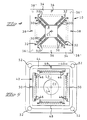
- the semiconductor device 8 is bonded to leads 30, only some of which are shown, attached to the film segment 10 and being electrically connected to contact pads 32 distributed about a center point C1 of the film segment 10, which is substantially square.
- Each slot in the film segment 10 is arranged substantially centrally of a respective one of the sides of the peripheral margin 34.
- each of the posts is, as seen in cross section, shorter than the length of the corresponding slot so that it is received with play therein in the longitudinal direction.
- the post closely fits the slot in the transverse direction thereof, that is to say it is a "line fit" across the slot.
- an insulating carrier 39 for the semiconductor device 8 on its film segment 10 is substantially square as seen in plan view, having a peripheral flange 40 extending about a seat, generally referenced 42, for the film segment 10, the seat 42 having a planar periphery 44.
- sets of electrical contact elements 46 are symmetrically distributed about the center point C2 of the seat 42, each for electrical conductive engagement with a respective one of the contact pads 32 on the film segment 10 when it is on the seat 42.
- each pocket being elongate in the direction of the center point C2 and the pockets of each pair being located on diametrically opposite sides of the point C2, each pocket of one pair being angularly spaced by 90° about the point C2 from each of the pockets of the other pair, in such a way that a line drawn L3 or L4 between each pair of opposite pockets passes through the center point C3.
- the pockets are accordingly located to receive the respective posts of the carrier 4.
- Each pocket 48 is dimensioned to receive its respective post with a snug fit in the transverse direction.
- the flange 40 is formed with openings 52 to receive fasteners (not shown) for securing it to a substrate, for example, a printed circuit board, not shown.
- Each contact element 46 has a tail 54 depending from the socket 39, for connection to electrical circuitry on the substrate or, if the socket is to be surface mounted, a contact (not shown) for engagement with a conductor pad on the surface of the substrate.
- the contact elements may for example be constructed according to the teaching of United States Patent Number 4,354,729, or United States Patent Number 4,513,353, both of which are incorporated herein by reference.
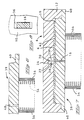
- the film segment 10 is first assembled to the carrier 4 by passing the posts 16 and 18 thereof through respective slots 36 and 38 of the film segment 10 so that the latter lies on the seat 6 of the carrier 4.
- the posts 16 are then inserted into respective pockets 48 of the sockets 39 and the posts 18 are inserted into respective pockets 50 of the socket 39 until film 10 lies on the seat 42 of the socket 39, as shown in Figure 7.
- the carrier 4 and the socket 39 are then in mating relationship with respective contact pads on the film 10 and in electrically conductive contact with respective contact elements 46 of the socket 39.
- the longitudinal play allowed for by the relative dimensions of the posts and the slots permits relative movement between the film 10 and the posts 16 and 18 under the action of humidity and temperature changes to which the electrical connector assembly comprising the carrier 4, the film segment 10 and the socket 39 will be subjected when in use.
- the said "line fit" between the posts and the longitudinal edges of the slots ensures that the parts of the assembly are always concentric.
- the posts will not break off their roots 20 during the assembly of the carrier 4 to the socket.
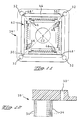
- the posts of the protective carrier 4′ are arranged at the corners of the margin 14′ and are referenced 16′ and 18′ of each pair are diametrically opposite to one another on either side of the center point C and are elongate theretowards as seen in plan view or in cross section, being arranged so that lines L1′ and 2′ drawn between the opposite posts of the post pairs 16′ and 18′, respectively, intersect the center point C.
- the posts of one pair 16′ or 18′ are angularly spaced by 90° about the center point C from each of the posts of the other pair 16′ or 18′.
- slots 36′ and 38′ are formed in a film segment to be used with the carrier of Figures 9 and 10, these slots being arranged to receive respective posts 16′ and 18′ therefore being arranged at the corners of the margin 34 of the film segment. They are positioned with respect to the center point C1 thereof in the same way as the posts of the pairs 16′ and 18′ are positioned relative to the center point C of the carrier 4′.
- the slots of the pairs 36′ and 38′ are dimensioned relative to the posts of the pairs 17′ and 18′ in the same way as the posts 16′ and 18′ of the carrier′ are dimensioned relative to the slots of the pairs 36′ and 38′ in the film segment.
- the socket 39′ is provided with pairs of opposed pockets 48′ and 50′ arranged at the corners of the periphery 44′ of the socket 39′ so as to be located for receiving the respective posts of the pairs 16′ and 18′, the pockets of the pairs 48′ and 50′ being dimensioned snugly to receive their posts.
Landscapes
- Engineering & Computer Science (AREA)
- Microelectronics & Electronic Packaging (AREA)
- Connecting Device With Holders (AREA)
- Wire Bonding (AREA)
- Connector Housings Or Holding Contact Members (AREA)
Applications Claiming Priority (2)
| Application Number | Priority Date | Filing Date | Title |
|---|---|---|---|
| US07/273,398 US4880386A (en) | 1988-11-18 | 1988-11-18 | Socketing a semiconductor device |
| US273398 | 1988-11-18 |
Publications (2)
| Publication Number | Publication Date |
|---|---|
| EP0369449A1 true EP0369449A1 (fr) | 1990-05-23 |
| EP0369449B1 EP0369449B1 (fr) | 1994-06-01 |
Family
ID=23043774
Family Applications (1)
| Application Number | Title | Priority Date | Filing Date |
|---|---|---|---|
| EP89121239A Expired - Lifetime EP0369449B1 (fr) | 1988-11-18 | 1989-11-16 | Socle pour composant semi-conducteur |
Country Status (5)
| Country | Link |
|---|---|
| US (1) | US4880386A (fr) |
| EP (1) | EP0369449B1 (fr) |
| JP (1) | JP2649278B2 (fr) |
| KR (1) | KR950013053B1 (fr) |
| DE (1) | DE68915702T2 (fr) |
Families Citing this family (2)
| Publication number | Priority date | Publication date | Assignee | Title |
|---|---|---|---|---|
| US5158467A (en) * | 1991-11-01 | 1992-10-27 | Amp Incorporated | High speed bare chip test socket |
| JP3514221B2 (ja) * | 2000-08-10 | 2004-03-31 | 株式会社デンソー | プリント配線基板 |
Citations (8)
| Publication number | Priority date | Publication date | Assignee | Title |
|---|---|---|---|---|
| FR2143934A1 (fr) * | 1971-07-01 | 1973-02-09 | Amp Inc | |
| US4007479A (en) * | 1976-03-29 | 1977-02-08 | Honeywell Information Systems, Inc. | Fixture for an integrated circuit chip |
| USRE30604E (en) * | 1979-03-05 | 1981-05-05 | Honeywell Information Systems Inc. | Reusable fixture for an integrated circuit chip |
| EP0055042A2 (fr) * | 1980-12-22 | 1982-06-30 | AMP INCORPORATED (a New Jersey corporation) | Borne de contact électrique précontrainte |
| US4513353A (en) * | 1982-12-27 | 1985-04-23 | Amp Incorporated | Connection of leadless integrated circuit package to a circuit board |
| US4696526A (en) * | 1985-07-26 | 1987-09-29 | Intel Corporation | Carrier for tape automated bonded semiconductor device |
| US4744009A (en) * | 1986-10-31 | 1988-05-10 | Amp Incorporated | Protective carrier and securing means therefor |
| US4768973A (en) * | 1987-07-02 | 1988-09-06 | Amp Incorporated | Removable retaining plate |
Family Cites Families (3)
| Publication number | Priority date | Publication date | Assignee | Title |
|---|---|---|---|---|
| US30604A (en) * | 1860-11-06 | Dyer greene | ||
| US4699593A (en) * | 1986-01-14 | 1987-10-13 | Amp Incorporated | Connector having contact modules for a substrate such as an IC chip carrier |
| US4684184A (en) * | 1986-01-14 | 1987-08-04 | Amp Incorporated | Chip carrier and carrier socket for closely spaced contacts |
-
1988
- 1988-11-18 US US07/273,398 patent/US4880386A/en not_active Expired - Fee Related
-
1989
- 1989-11-13 JP JP1292550A patent/JP2649278B2/ja not_active Expired - Lifetime
- 1989-11-15 KR KR1019890016530A patent/KR950013053B1/ko not_active Expired - Fee Related
- 1989-11-16 DE DE68915702T patent/DE68915702T2/de not_active Expired - Fee Related
- 1989-11-16 EP EP89121239A patent/EP0369449B1/fr not_active Expired - Lifetime
Patent Citations (8)
| Publication number | Priority date | Publication date | Assignee | Title |
|---|---|---|---|---|
| FR2143934A1 (fr) * | 1971-07-01 | 1973-02-09 | Amp Inc | |
| US4007479A (en) * | 1976-03-29 | 1977-02-08 | Honeywell Information Systems, Inc. | Fixture for an integrated circuit chip |
| USRE30604E (en) * | 1979-03-05 | 1981-05-05 | Honeywell Information Systems Inc. | Reusable fixture for an integrated circuit chip |
| EP0055042A2 (fr) * | 1980-12-22 | 1982-06-30 | AMP INCORPORATED (a New Jersey corporation) | Borne de contact électrique précontrainte |
| US4513353A (en) * | 1982-12-27 | 1985-04-23 | Amp Incorporated | Connection of leadless integrated circuit package to a circuit board |
| US4696526A (en) * | 1985-07-26 | 1987-09-29 | Intel Corporation | Carrier for tape automated bonded semiconductor device |
| US4744009A (en) * | 1986-10-31 | 1988-05-10 | Amp Incorporated | Protective carrier and securing means therefor |
| US4768973A (en) * | 1987-07-02 | 1988-09-06 | Amp Incorporated | Removable retaining plate |
Also Published As
| Publication number | Publication date |
|---|---|
| KR900008725A (ko) | 1990-06-04 |
| JPH02218151A (ja) | 1990-08-30 |
| DE68915702T2 (de) | 1994-09-15 |
| DE68915702D1 (de) | 1994-07-07 |
| US4880386A (en) | 1989-11-14 |
| EP0369449B1 (fr) | 1994-06-01 |
| JP2649278B2 (ja) | 1997-09-03 |
| KR950013053B1 (ko) | 1995-10-24 |
Similar Documents
| Publication | Publication Date | Title |
|---|---|---|
| US4744009A (en) | Protective carrier and securing means therefor | |
| US4832612A (en) | Protective carrier and securing means therefor | |
| US4843313A (en) | Integrated circuit package carrier and test device | |
| US6836003B2 (en) | Integrated circuit package alignment feature | |
| US5205741A (en) | Connector assembly for testing integrated circuit packages | |
| US4195193A (en) | Lead frame and chip carrier housing | |
| US3825876A (en) | Electrical component mounting | |
| US5131852A (en) | Electrical socket | |
| JP3325060B2 (ja) | 電気コネクタ | |
| KR970000291Y1 (ko) | 표면 장착 전기 커넥터 어셈블리 | |
| US5884395A (en) | Assembly structure for making integrated circuit chip probe cards | |
| EP0516402A1 (fr) | Substrat muni de lignes électriques et son procédé de fabrication | |
| US5456018A (en) | Alignment system for planar electronic devices arranged in parallel fashion | |
| KR20010053507A (ko) | Ic 소켓 | |
| EP0311513B1 (fr) | Segment de film ayant une puce de circuit intégré soudé dessus et sa fixation | |
| US4331373A (en) | Modular system with system carrier, test carrier and system connector | |
| US4648666A (en) | Electrical connector | |
| EP0369449B1 (fr) | Socle pour composant semi-conducteur | |
| US5429511A (en) | Stackable interconnection socket | |
| JPH0638463B2 (ja) | 電子パッケージ | |
| EP0145327A2 (fr) | Arrangement d'interface électrique | |
| US5813869A (en) | IC socket and guide member | |
| JPH07230837A (ja) | 混成集積回路基板用端子 | |
| KR100246360B1 (ko) | 마이크로 비지에이 패키지 | |
| JP2000195630A (ja) | Icソケット |
Legal Events
| Date | Code | Title | Description |
|---|---|---|---|
| PUAI | Public reference made under article 153(3) epc to a published international application that has entered the european phase |
Free format text: ORIGINAL CODE: 0009012 |
|
| AK | Designated contracting states |
Kind code of ref document: A1 Designated state(s): DE FR GB |
|
| 17P | Request for examination filed |
Effective date: 19901109 |
|
| 17Q | First examination report despatched |
Effective date: 19920630 |
|
| RAP1 | Party data changed (applicant data changed or rights of an application transferred) |
Owner name: THE WHITAKER CORPORATION |
|
| GRAA | (expected) grant |
Free format text: ORIGINAL CODE: 0009210 |
|
| AK | Designated contracting states |
Kind code of ref document: B1 Designated state(s): DE FR GB |
|
| REF | Corresponds to: |
Ref document number: 68915702 Country of ref document: DE Date of ref document: 19940707 |
|
| ET | Fr: translation filed | ||
| PLBE | No opposition filed within time limit |
Free format text: ORIGINAL CODE: 0009261 |
|
| STAA | Information on the status of an ep patent application or granted ep patent |
Free format text: STATUS: NO OPPOSITION FILED WITHIN TIME LIMIT |
|
| 26N | No opposition filed | ||
| PGFP | Annual fee paid to national office [announced via postgrant information from national office to epo] |
Ref country code: GB Payment date: 19971007 Year of fee payment: 9 |
|
| PGFP | Annual fee paid to national office [announced via postgrant information from national office to epo] |
Ref country code: FR Payment date: 19971106 Year of fee payment: 9 |
|
| PGFP | Annual fee paid to national office [announced via postgrant information from national office to epo] |
Ref country code: DE Payment date: 19971127 Year of fee payment: 9 |
|
| PG25 | Lapsed in a contracting state [announced via postgrant information from national office to epo] |
Ref country code: GB Free format text: LAPSE BECAUSE OF NON-PAYMENT OF DUE FEES Effective date: 19981116 |
|
| GBPC | Gb: european patent ceased through non-payment of renewal fee |
Effective date: 19981116 |
|
| PG25 | Lapsed in a contracting state [announced via postgrant information from national office to epo] |
Ref country code: FR Free format text: LAPSE BECAUSE OF NON-PAYMENT OF DUE FEES Effective date: 19990730 |
|
| REG | Reference to a national code |
Ref country code: FR Ref legal event code: ST |
|
| PG25 | Lapsed in a contracting state [announced via postgrant information from national office to epo] |
Ref country code: DE Free format text: LAPSE BECAUSE OF NON-PAYMENT OF DUE FEES Effective date: 19990901 |