EP0369843A1 - Zentrale Datenverarbeitungseinheit mit mehreren Prozessoren und mehreren Speichern für ein Datenverarbeitungssystem - Google Patents
Zentrale Datenverarbeitungseinheit mit mehreren Prozessoren und mehreren Speichern für ein Datenverarbeitungssystem Download PDFInfo
- Publication number
- EP0369843A1 EP0369843A1 EP19890402917 EP89402917A EP0369843A1 EP 0369843 A1 EP0369843 A1 EP 0369843A1 EP 19890402917 EP19890402917 EP 19890402917 EP 89402917 A EP89402917 A EP 89402917A EP 0369843 A1 EP0369843 A1 EP 0369843A1
- Authority
- EP
- European Patent Office
- Prior art keywords
- station
- input
- request
- output
- requests
- Prior art date
- Legal status (The legal status is an assumption and is not a legal conclusion. Google has not performed a legal analysis and makes no representation as to the accuracy of the status listed.)
- Granted
Links
Images




Classifications
-
- G—PHYSICS
- G06—COMPUTING OR CALCULATING; COUNTING
- G06F—ELECTRIC DIGITAL DATA PROCESSING
- G06F15/00—Digital computers in general; Data processing equipment in general
- G06F15/76—Architectures of general purpose stored program computers
- G06F15/80—Architectures of general purpose stored program computers comprising an array of processing units with common control, e.g. single instruction multiple data processors
- G06F15/8053—Vector processors
- G06F15/8092—Array of vector units
-
- G—PHYSICS
- G06—COMPUTING OR CALCULATING; COUNTING
- G06F—ELECTRIC DIGITAL DATA PROCESSING
- G06F15/00—Digital computers in general; Data processing equipment in general
- G06F15/76—Architectures of general purpose stored program computers
- G06F15/80—Architectures of general purpose stored program computers comprising an array of processing units with common control, e.g. single instruction multiple data processors
- G06F15/8007—Architectures of general purpose stored program computers comprising an array of processing units with common control, e.g. single instruction multiple data processors single instruction multiple data [SIMD] multiprocessors
Definitions
- the invention relates to the field of information processing systems and in particular high performance systems using several processors which can operate simultaneously to execute a common program.
- the invention relates more particularly to a central unit architecture which can serve as a vector unit of a vector computer.
- the performance of a system also depends on the performance of the memories with which the processors must communicate.
- the performance of a memory or a set of memories is defined by its access time and its cycle time.
- Access time is defined as the time interval between the sending of a request by one of the processors and the appearance of an acknowledgment signal indicating that the request is taken into account by the memory and thus a new request can be addressed to him.
- Cycle time defines the time interval between when a request is received by memory and when the response is available in the memory output register.
- a conventional solution consists in using a memory made up of several modules and in performing interleaved addressing of these modules. According to this interleaving technique, successive or simultaneous requests sent by the processors are addressed successively or simultaneously to different modules of the memory.
- the bus solution shared by processors and memories prohibits simultaneous exchanges between several processors and several memories.
- the bus is therefore unsuitable for parallel operation.
- the most commonly used solution consists in providing an interconnection network of the "crossbar" or derivative type which allows these simultaneous links. This solution is however limited by the increase in the complexity of the interconnection device when the cycle times decrease and when the parallelization rate increases.
- a "crossbar" network implies a centralization of the paths which has the following unfavorable effects: - increased connectivity which is all the more important when the paths are wide; - longer connections when the memory size increases, with an unfavorable effect on bit rates and access times; - difficult integration because the percentage of connection is high compared to the associated logical functions; - need for centralized order management, which leads to difficulties in managing data flows and conflicts; - lack of modularity; - difficulty in implementing redundancies to allow reconfigurations.
- the invention aims to remedy these drawbacks and more particularly to provide a device ensuring the same connection possibilities as a "crossbar" network and having the same peak flow.
- each processor sends a request containing an address making it possible to identify the memory concerned.
- the connection between the processors and the memories is carried out by means of a ring of stations which can operate in looped shift register of which each stage can memorize a request, this request being accompanied by a validity indicator.
- the output of each station is connected, directly or indirectly, to the input interface of a memory.
- each station can be accessed, under the control of a station control device, by requests from an associated processor.
- the proposed solution presents a decentralized management and a distributed physical implantation making the realization and the modularity easier.
- the reconfiguration possibilities are more flexible.
- the subject of the invention is a central unit for a data processing system comprising several processors connected to several memories, said processors operating as transmitters of requests while the memories operate as receivers of said requests, said requests comprising control information, addressing and possibly data, input interconnection means being provided for transmitting to said memories the requests from said processors, output interconnection means being provided for transmitting to said processors the responses from said memories to said requests, said means for input interconnection comprising several parallel input interfaces, each input interface providing for each request received a request acknowledgment signal representative of the acceptance by said input interface of said received request, said central unit being features e in that each request is associated with a request indicator whose logical value is representative of the validity of the associated request, in that the input interconnection means comprise input stations each associated with a processor and to an input interface, in that each station includes at least one register capable of storing a request and its associated request indicator, a first access input to said register and an output connected to the output of said register, in that said stations are connected in cascade, the output of the last
- each parallel interface is simply constituted by the input interface of a memory.
- the processors will not be able to transmit for two clock cycles for each accepted request.
- the number of station rings is increased so as to increase the average bit rate in the case of unframed requests.
- the central unit is further characterized in that said input interconnection device is formed of several rings of stations arranged in as many levels, each ring of stations being identical to said ring of input stations, said ring of input stations constituting the first level, said parallel input interfaces then being formed by the ring of stations of the second level, in that for each memory a memory input interface delivers a memory acknowledgment signal, in that each station of the last level has its output connected to the input interface of an associated memory and receives on its acknowledgment input the memory acknowledgment signal from the memory input interface which is connected to the station of said last level and which is located upstream of said station, in that each station of another level has its output connected to the second input of a station belonging to the level directly higher and receives on its acknowledgment input the notification signal from the station located upstream of said station belonging to said directly higher level.
- the first consists in using only two station rings, which has the advantage of a simplification of construction.
- Another interesting case consists in using a number of stations equal to the number of processors and memories. This solution promotes communication between each processor and its associated memory.
- the invention also relates to a central unit characterized in that said output interconnection device is identical to one of the input interconnection devices as defined above, the respective roles of the processors and of the memories being inverted, the memories functioning as transmitters of responses, the processors functioning as receptors of responses, said responses being accompanied by an indicator of validity of the responses.
- FIG. 1 represents the general diagram of a central unit of conventional type and which can serve as a framework for the invention.
- the central unit comprises a processing unit P generally consisting of several processors operating in parallel, each processor being able to be organized in "pipeline".
- the processing unit P communicates with a set M of memories.
- the assembly M can comprise a plurality of memories, usually called logical banks, having independent accesses, each logical bank being able to be constituted by a plurality of modules or physical banks interleaved.
- the processors simultaneously generate memory requests which are available in parallel in the output interfaces of the ISP processors. These requests are transferred to the input interfaces of the IEM memories via an XE input interconnection system, the role of which is also to manage the conflicts that may arise.
- the set M of memories Depending on the requests received, the set M of memories provides the corresponding responses in ISM output interfaces. These responses are transmitted, via an output interconnection device XS, to the input interfaces IEP of the processing unit P.
- the output interconnection device XS has a role completely symmetrical to that of XE input.
- unit P communicates with the outside by means of input-output units not shown.
- the solution consists in using as an interconnection device a system of “crossbar” type produced by means of a plurality of multiplexers. Its management is carried out using associated logic.
- this solution has limits which are linked to the parallelization rate, the frequency of transmission of requests and responses, as well as the width of the data paths.
- the problem of conflict management becomes very difficult to solve when the number of processors and memories becomes high. The following description will show how the invention solves this problem.
- n processors P1, ... P i-1 , P i , ... P n constitute the processing unit P of FIG. 1.
- the set M of memories is constituted by n logical banks M1 , ... M i-1 , M i , ... M n .
- the logical benches M i will be more simply designated under the name "memory”.
- Each processor has an output interface IS1, ... IS i-1 , IS i , ... IS n .
- These IS i interfaces serve both as output buffers for available requests and as control devices vis-à-vis the processors and the XE input interconnection device.
- the XE input interconnection device comprises an IE input interface made up of several parallel input interfaces IE1, ... IE i-1 , IE i , ... IE n .
- Each input interface IE i receives requests from the processors.
- an IE i interface accepts a request present at its input, it sends an acknowledgment signal N2 i to signal whether this request is accepted by the interface or not.
- the input interconnection device XE also comprises a set of input stations ST1, ... ST i-1 , ST i , ... ST n .
- Each station ST i contains at least one register 1 capable of storing requests.
- Each station has a first input 2 and an output 3 connected to the output of the register 1.
- These stations are connected in cascade, the output of the last station ST n being connected to the first input of the first station ST1 so as to allow the station registers to operate, under the action of a clock signal not shown, in looped shift register.
- station ring AS1 this set of stations ST i .
- the output 3 of each station ST i is on the other hand connected to an associated input interface IE i .
- Each station ST i also has a second input 4 connected to the output interface IS i of an associated processor P i .
- Each station ST i is also provided with a control device, not shown, making it possible to selectively put the entry of register 1 into communication with the first entry 2 or the second entry 4 of the station.
- the output interfaces IS i , the input interfaces IE i are controlled by the clock signal already mentioned.
- each request is accompanied by a validity indicator B which can be supplied by the processor which issues the request.
- the control device of each station ST i receives by an acknowledgment input 7 the acknowledgment signal N2 i-1 delivered by the downstream interface IE i-1 as well as the indicator B contained in the downstream station ST i- 1 .
- Each station ST i finally comprises a notification output 8 connected to the output interface IS i of the associated processor.
- the device of Figure 2 operates as follows.
- the requests contained in the registers are assumed to be all invalid.
- the indicator B associated with each request contained in the ring AS 1 has a first logical value which indicates an invalid associated request.
- each processor P i-1 places a valid request in its output interface IS i-1 .
- the control device of the associated station ST i-1 detects that the request contained in the upstream register is not valid and authorizes the transfer of the request from the processor P i-1 to the register 1 of the station.
- each register contains a valid request.
- the request contained in the ST i-1 station is presented to the IE i-1 input interface. If this request is indeed intended for the interface, the latter delivers an acknowledgment signal N2 i-1 having a first logical value signifying the acceptance of the request by the interface. During this time, a subsequent request is present in the output interface of the processor P i .
- the associated station ST i detects the indicator B of the request contained in the upstream station ST i-1 .
- the indicator signaling a valid request the station ST i is informed. But the station ST i receives the acknowledgment signal N2 i-1 from the downstream interface IE i-1 indicating that this request will be accepted by the interface.
- the control device of the station ST i will therefore authorize the transfer of the new request from the processor P i to its associated register.
- the register of the ST station i-1 would contain a request which is not intended for the IE interface i-1 .
- the acknowledgment signal N2 i-1 will then take another logic value corresponding to this situation.
- the downstream station ST i will take this into account and inform the processor P i of this situation by a notification signal N i originating from the output 8 and delivered by the control device of the station ST i .
- the notification signal N i will therefore prevent the processor P i from issuing a new request in the following cycle.
- the request contained in the register of station ST i-1 will then be transferred to the register of station ST i .
- FIG. 3 represents an exemplary embodiment of the stations ST i .
- the register 1 of the station ST i comprises several flip-flops controlled by the clock signal h. One of the flip-flops is assigned to the indicator B.
- the output of register 1 constitutes output 3 of the station.
- the control device 5 comprises a selection device such as a multiplexer 9 and a control device formed by the logic circuits 10 and 11.
- the input of the register 1 is connected to the output of the multiplexer 9 including a first input "0 "is connected to the first input 2 of the station and a second input" 1 "of which is connected to the second input 4 of the station.
- the multiplexer 9 is controlled by a binary selection signal S supplied by the control device 10 and 11. When the signal S takes the logic value 1, the multiplexer 9 puts the input 4 in communication with the input of the register 1. If S is 0, entry 2 is put in communication with the entry of register 1.
- the control device consists of an inverter 11 whose input 6 receives the indicator B contained in the downstream station.
- the output of the inverter 11 is connected to a first input of an OR gate 10, the second input of which is connected to the acknowledgment input 7 of the station.
- the OR gate 10 then delivers the selection signal S described above. This signal S is also applied to the notification output 8 of the station and will therefore also constitute the notification signal N i .
- the simplest embodiment of the device in FIG. 2 consists in using the input interfaces of the memories directly as parallel input interfaces IE i .
- This solution has the advantage of simplicity of implementation but has the drawback of lowering the speed in the case of unframed requests.
- each processor P i does not address its associated memory M i but the memory M i + d .
- the processors After sending a first request, the processors will be blocked for d cycle time before being able to issue their next request. This results in a drop in flow which is all the more significant the larger the cropping d.
- this problem can be solved by adding additional station rings.
- the first ring of stations AS1 is identical to that described in FIG. 2 and the input interface IE is now produced by means of a second ring of stations AS2 identical to the first ring AS1.
- Each station ST i of the first ring AS1 has its output 3 connected to the second input 4 of a peer station ST2 i of the second ring AS2.
- the acknowledgment input 7 of the station ST i receives the signal N2 i-1 from the station ST2 i-1 placed directly upstream of the peer station ST2 i .
- This signal N2 i-1 comes from the notification output 8 of the station ST2 i-1 .
- each station ST2 i of the second ring AS2 is connected to the input interface IEM i of an associated memory M i .
- the acknowledgment input 7 of the station ST2 i is connected to the acknowledgment output ACK i-1 of the memory M i-1 located downstream.
- the notification signal N2 i delivered by a station ST2 i of the second ring replaces the acknowledgment signal of a parallel interface IE i of the Figure 2.
- the acknowledgment signal ACK i-1 from the IEM interface i-1 of a memory M i-1 constitutes the acknowledgment signal for the station ST2 i which is placed directly downstream of this memory and which belongs to the second ring AS2.
- each station gives absolute priority to the upstream station on the same ring; - if the upstream station is free, or if it becomes available (acceptance of the request by the associated memory or by the associated upper station), a request is transferred to the station in question from the first ring or from a processor ; - if a request presented to a memory is not intended for him or if a request intended for a memory is presented to him while this memory is occupied, this request remains on the ring and will be represented in memory after a complete revolution in the 'ring; - the indicator B accompanies each request and makes it possible to determine whether the station which contains it is free or not.
- the output of the stations ST i is not simply connected to the input interface of a memory.
- the additional ring allows a more advantageous behavior in the case of framed requests. Indeed, initially this system authorizes for each processor the emission of two successive unframed requests. Then the processors are blocked during d cropping cycles during which all the requests contained in the stations shift by d stages to the right. Then, two new successive unframed requests can be issued by the processors. As a result, the overall throughput is improved because each crop cycle causes the shift of twice as many requests as in the case of a single ring.
- Figure 5 partially shows an embodiment using q rings: AS1, ... AS j , AS j + 1 , ... AS q .
- These rings are arranged in q levels, the ring AS1 of the first level being connected to the processors, while the ring AS q of level q communicates directly with the memories.
- the AS1 ring of the first level is the same as before.
- the arrangement of the last ring AS q with respect to the memories is identical to that of the ring AS2 in FIG. 4.
- each station STj i is identified by a double index j i where j is the level to which the station belongs, i being the rank of the station in its ring AS j .
- Each station STj i of an intermediate level j (j different from q) is associated with a station ST (j + 1) i of the same rank i and of higher level j + 1.
- each station STj i has its output 3 connected to the input 4 of the associated station ST (j + 1) i of the upper level j + 1.
- the station STj i receives on its acknowledgment input 7 the notification signal N (j + 1) (i-1) coming from the notification output 8 of the station ST (j + 1) (i-1) of the level upper j + 1 and located upstream.
- FIG. 6 shows in detail the links between two neighboring stations STq i , STq (i + 1) of the last level q with the input interface IEM i of the memory M i .
- Register 1 of station STq i consists of a first flip-flop B assigned to the validity indicator, one or more flip-flops F corresponding to the function code associated with the request, several flip-flops DT to store a label d origin or data, of several AD flip-flops to store the address associated with the request, the least significant PF of the address AD used to identify the memory concerned by the address.
- the outputs of these flip-flops constitute output 3 of the station STq i .
- These flip-flops are controlled by the clock signal h.
- the IEM interface i comprises an input register 12 and a decoder 13 connected to the output 3.
- the decoder 13 receives the least significant PF from the address and delivers a signal SEL taking the logic value 1 when the least significant PF received coincide with the identity of the memory M i .
- the input register 12 receives the rest of the request contained in the register 1.
- the flip-flop BM of the register 12 is assigned to the indicator B.
- the output of the flip-flop BM is applied to the input of an inverter 15 whose the output is connected to a first input of an AND gate 14.
- the second input of gate 14 receives the signal SEL from the decoder 13.
- the AND gate 14 delivers the acknowledgment signal ACK i from the memory M i .
- the register 12 is of a conventional type, comprising parallel inputs and outputs, a clock input, a loading command input and a reset input.
- Register 12 receives the clock signal h on its clock input and the signal ACK i on its loading control input. Its reset input receives the reset signal from a free memory detection circuit 17. The output of register 12 communicates with the memory input.
- the interface circuit operates as follows. When the memory becomes free, the circuit 17 forces the reset signal to a logic value which resets the register 12 to zero. If a request contained in the register 1 is intended for the memory, the output SEL of the decoder 13 takes the value 1. As BM is equal to 0, the output of the inverter 15 takes the value 1. As a result, ACK i is equal to 1. The register 12 is therefore authorized to load at the next clock pulse. After loading the request, as long as the reset signal has not reappeared, BM retains the value of indicator B. If B was 0, a new request can be loaded in the next cycle, without waiting for the reset. If on the other hand B was equal to 1, a subsequent request can only be taken into account after the reset signal has appeared.
- the interconnection according to the invention makes it possible to solve the problem of unframed requests with a drop in performance which can be limited by increasing the number of rings.
- Another cause of drop in speed in the interconnection device is related to the problems of saturation of the rings and memory conflicts.
- a buffer memory 16 of the "first in - first out” (FIFO) type which will make it possible to absorb requests in memory in the event that requests that are too closely spaced address the same physical bench. The saturation of the rings will be avoided.
- a buffer of this type could also be provided at the output of the memories so that saturation at the level of the responses does not cause saturation of the input rings. Since buffers of the "FIFO" type are well known per se, there is no need to give one. detailed description. It can however be noted that the circuit 17 generates the RESET signal as a function of a signal indicating whether the buffer 16 is saturated or not.
- the solutions described above can be transposed to the output interconnection device.
- the responses from the briefs will be accompanied by an indicator for the validity of the responses B r .
- These responses will be conveyed by response rings composed of the same elements as the request rings described above.
- Each ring therefore defines a direction of circulation of requests and, by convention, this direction corresponds to the increasing order of the indices i of the processors P i and of the memories M i .
- the same arrangement is used as for the request rings. If we suppose, to simplify the reasoning, that the input interconnection has the same number q of levels as the output interconnection, we can see that for well-framed requests, the minimum number of stages crossed by requests or by responses equals q. However, the cycle time for a memory access is equal to the sum of the cycle time of a memory and of a transmission time of a request to the memory and of the response to the processor which issued the request.
- the transmission time therefore the cycle time for a framed memory access is independent of the framing.
- This property can be advantageous when it is desired that the order of arrival of the responses is the same as that of the requests in the case of a non-zero framing.
- the framed requests are favored in cycle time.
- the shortest path (q stages) is no longer chosen to connect the output of a memory M i to its associated processor P i but to connect it to the processor of higher index P i + 1 .
- the number of output stages to cross is equal to n-1-d.
- the total transmission time is therefore proportional to n-1, whatever the cropping between 0 and n-1 .
- the direction of circulation of the responses is reversed, that is to say that it corresponds to the order of the increasing indices for the memories and to the order of the decreasing indices for the processors.
- the number of output stages to cross is equal to 2q for the framed requests, if the shortest path is chosen to connect the output of a memory M i to its associated processor P i .
- the number of output stages to be crossed is equal to d + q.
- the total transmission time is therefore proportional to 2d + 2q.
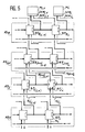
- FIG. 7 shows a complete embodiment of a central unit according to the invention in the case where the input and output interconnection devices each comprise two rings. We find in this figure the elements already described above, with the same references. The direction of circulation of responses is the opposite of that of requests.
- processor P1 it transmits its requests through the station ST1 of the ring AS1. If the station ST21 of the second ring is available, the request contained in the station ST1 is transmitted to the next cycle to ST21. Otherwise, the request is transmitted to the downstream station ST2 of the first ring.
- a request contained in the station ST21 is accepted by the memory M1, this releases the station ST22.
- this request is transferred to this station. If the station STR21 of the second ASR2 response ring is available, this request is transferred to the next cycle in the station STR21 which presents it to the input interface of the processor P1.
- Figure 7 also shows an arrangement of the processors and memories which facilitates the connection. This example also illustrates the modular nature of the embodiments permitted by the invention.
Landscapes
- Engineering & Computer Science (AREA)
- Computer Hardware Design (AREA)
- Theoretical Computer Science (AREA)
- Computing Systems (AREA)
- Physics & Mathematics (AREA)
- General Engineering & Computer Science (AREA)
- General Physics & Mathematics (AREA)
- Multi Processors (AREA)
Applications Claiming Priority (2)
| Application Number | Priority Date | Filing Date | Title |
|---|---|---|---|
| FR8813904A FR2638259A1 (fr) | 1988-10-25 | 1988-10-25 | Unite centrale a plusieurs processeurs et plusieurs memoires pour systemes de traitement de donnees |
| FR8813904 | 1988-10-25 |
Publications (2)
| Publication Number | Publication Date |
|---|---|
| EP0369843A1 true EP0369843A1 (de) | 1990-05-23 |
| EP0369843B1 EP0369843B1 (de) | 1994-05-18 |
Family
ID=9371237
Family Applications (1)
| Application Number | Title | Priority Date | Filing Date |
|---|---|---|---|
| EP19890402917 Expired - Lifetime EP0369843B1 (de) | 1988-10-25 | 1989-10-24 | Zentrale Datenverarbeitungseinheit mit mehreren Prozessoren und mehreren Speichern für ein Datenverarbeitungssystem |
Country Status (4)
| Country | Link |
|---|---|
| EP (1) | EP0369843B1 (de) |
| JP (1) | JP2589828B2 (de) |
| DE (1) | DE68915400T2 (de) |
| FR (1) | FR2638259A1 (de) |
Families Citing this family (1)
| Publication number | Priority date | Publication date | Assignee | Title |
|---|---|---|---|---|
| DE4227634A1 (de) * | 1992-08-18 | 1994-02-24 | Siemens Ag | Tür für einen Schaltschrank mit einem an der Innenseite anzubringenden Rahmen |
Citations (3)
| Publication number | Priority date | Publication date | Assignee | Title |
|---|---|---|---|---|
| US3735362A (en) * | 1971-09-22 | 1973-05-22 | Ibm | Shift register interconnection system |
| US4334305A (en) * | 1979-02-15 | 1982-06-08 | Cselt - Centro Studi E Laboratori Telecomunicazioni S.P.A. | Data-handling system with operatively interconnected processors |
| EP0201088A2 (de) * | 1985-05-10 | 1986-11-12 | Hitachi, Ltd. | Parallelrechner |
-
1988
- 1988-10-25 FR FR8813904A patent/FR2638259A1/fr active Granted
-
1989
- 1989-10-24 DE DE1989615400 patent/DE68915400T2/de not_active Expired - Fee Related
- 1989-10-24 EP EP19890402917 patent/EP0369843B1/de not_active Expired - Lifetime
- 1989-10-25 JP JP1278324A patent/JP2589828B2/ja not_active Expired - Fee Related
Patent Citations (3)
| Publication number | Priority date | Publication date | Assignee | Title |
|---|---|---|---|---|
| US3735362A (en) * | 1971-09-22 | 1973-05-22 | Ibm | Shift register interconnection system |
| US4334305A (en) * | 1979-02-15 | 1982-06-08 | Cselt - Centro Studi E Laboratori Telecomunicazioni S.P.A. | Data-handling system with operatively interconnected processors |
| EP0201088A2 (de) * | 1985-05-10 | 1986-11-12 | Hitachi, Ltd. | Parallelrechner |
Non-Patent Citations (1)
| Title |
|---|
| K. HWANG et al.: "Computer architecture and parallel processing", 1984, pages 145-164, McGraw-Hill Book Co., US * |
Also Published As
| Publication number | Publication date |
|---|---|
| JP2589828B2 (ja) | 1997-03-12 |
| EP0369843B1 (de) | 1994-05-18 |
| JPH02171879A (ja) | 1990-07-03 |
| DE68915400T2 (de) | 1994-10-06 |
| FR2638259A1 (fr) | 1990-04-27 |
| FR2638259B1 (de) | 1995-03-17 |
| DE68915400D1 (de) | 1994-06-23 |
Similar Documents
| Publication | Publication Date | Title |
|---|---|---|
| EP0104293B1 (de) | Anordnung zum Laden und Lesen verschiedener Kippschaltungsketten in einem Datenverarbeitungssystem | |
| FR2667706A1 (fr) | Antememoire hierarchique a circuits integres. | |
| EP0558125B1 (de) | Neuronaler Prozessor mit verteilten synaptischen Zellen | |
| FR2617304A1 (fr) | Sequenceur d'entrees/sorties programmable pour processeur d'entree/sortie | |
| EP0021917A1 (de) | Terminal-Konzentrator für Datenpaketübertragungs- und -vermittlungsnetz | |
| FR2713422A1 (fr) | Procédé de conversion automatique pour le portage d'applications de télécommunication du réseau TCP/IP sur le réseau OSI-CO et module utilisé dans ledit procédé. | |
| FR2820921A1 (fr) | Dispositif et procede de transmission dans un commutateur | |
| EP0920157A1 (de) | Verwaltungseinrichtung eines gemeinsamen Pufferspeichers | |
| FR2571565A1 (fr) | Procede et dispositif de selection d'un bit d'adresse dans un reseau de commutation de paquets | |
| EP0020255B1 (de) | Vermittlungsebene eines Operators für Datenpaketvermittlungsnetz | |
| FR2948206A1 (fr) | Dispositif et procede pour l'execution distribuee de traitements de donnees numeriques | |
| EP0369843B1 (de) | Zentrale Datenverarbeitungseinheit mit mehreren Prozessoren und mehreren Speichern für ein Datenverarbeitungssystem | |
| EP0782815B1 (de) | Vorrichtung zur verwaltung von verbindungen zwischen objekten | |
| EP0359607B1 (de) | Zentrale Datenverarbeitungseinheit für ein Datenverarbeitungssystem | |
| EP0344052B1 (de) | Modularer Speicher | |
| EP0771130B1 (de) | Multiplex- und Zuweisungsgerät für ein ATM-Netzwerk | |
| EP0346420B1 (de) | Verfahren zum informationsaustausch in einem mehrprozessorsystem | |
| EP0974902B1 (de) | Verfahren um Fehler auf einer seriellen Verbindung einer integrierten Schaltung zu erkennen und Vorrichtung zur Durchführung des Verfahrens | |
| EP0589743B1 (de) | Modulare Vorrichtung zum Koppeln und zum Multiplexen von unterschiedlichen Bussen | |
| EP0379436A1 (de) | Anordnung und Verfahren zur Anforderungsarbitrierung und zur Auflösung von Konflikten, verbunden mit Zugriff zu Speichern mit unabhängigen Bereichen für Computergeräte | |
| EP0333537A1 (de) | Digitale Signalverarbeitungsanordnung | |
| FR2753030A1 (fr) | Equipement de serveur d'acces | |
| FR2742894A1 (fr) | Systeme d'echange d'informations entre plusieurs operateurs | |
| EP0512882A1 (de) | Erkennungsverfahren und Steuerungsanordnung einer zu einem Empfänger gesendeten digitalen Nachrichtenform | |
| EP0011540A1 (de) | Ein-/Ausgabe-Schnittstelle zwischen einem Datenvermittler und mehreren Übertragungsleitungen |
Legal Events
| Date | Code | Title | Description |
|---|---|---|---|
| PUAI | Public reference made under article 153(3) epc to a published international application that has entered the european phase |
Free format text: ORIGINAL CODE: 0009012 |
|
| AK | Designated contracting states |
Kind code of ref document: A1 Designated state(s): DE FR GB IT NL |
|
| 17P | Request for examination filed |
Effective date: 19900411 |
|
| RAP3 | Party data changed (applicant data changed or rights of an application transferred) |
Owner name: BULL S.A. |
|
| 17Q | First examination report despatched |
Effective date: 19931026 |
|
| GRAA | (expected) grant |
Free format text: ORIGINAL CODE: 0009210 |
|
| AK | Designated contracting states |
Kind code of ref document: B1 Designated state(s): DE FR GB IT NL |
|
| GBT | Gb: translation of ep patent filed (gb section 77(6)(a)/1977) |
Effective date: 19940524 |
|
| REF | Corresponds to: |
Ref document number: 68915400 Country of ref document: DE Date of ref document: 19940623 |
|
| ITF | It: translation for a ep patent filed | ||
| PLBE | No opposition filed within time limit |
Free format text: ORIGINAL CODE: 0009261 |
|
| STAA | Information on the status of an ep patent application or granted ep patent |
Free format text: STATUS: NO OPPOSITION FILED WITHIN TIME LIMIT |
|
| 26N | No opposition filed | ||
| REG | Reference to a national code |
Ref country code: GB Ref legal event code: IF02 |
|
| PGFP | Annual fee paid to national office [announced via postgrant information from national office to epo] |
Ref country code: FR Payment date: 20050831 Year of fee payment: 17 |
|
| PGFP | Annual fee paid to national office [announced via postgrant information from national office to epo] |
Ref country code: GB Payment date: 20050926 Year of fee payment: 17 |
|
| PGFP | Annual fee paid to national office [announced via postgrant information from national office to epo] |
Ref country code: DE Payment date: 20051004 Year of fee payment: 17 |
|
| PGFP | Annual fee paid to national office [announced via postgrant information from national office to epo] |
Ref country code: IT Payment date: 20061031 Year of fee payment: 18 |
|
| PG25 | Lapsed in a contracting state [announced via postgrant information from national office to epo] |
Ref country code: DE Free format text: LAPSE BECAUSE OF NON-PAYMENT OF DUE FEES Effective date: 20070501 |
|
| GBPC | Gb: european patent ceased through non-payment of renewal fee |
Effective date: 20061024 |
|
| PG25 | Lapsed in a contracting state [announced via postgrant information from national office to epo] |
Ref country code: GB Free format text: LAPSE BECAUSE OF NON-PAYMENT OF DUE FEES Effective date: 20061024 |
|
| PGFP | Annual fee paid to national office [announced via postgrant information from national office to epo] |
Ref country code: NL Payment date: 20070924 Year of fee payment: 19 |
|
| REG | Reference to a national code |
Ref country code: FR Ref legal event code: ST Effective date: 20080630 |
|
| PG25 | Lapsed in a contracting state [announced via postgrant information from national office to epo] |
Ref country code: FR Free format text: LAPSE BECAUSE OF NON-PAYMENT OF DUE FEES Effective date: 20071031 |
|
| PG25 | Lapsed in a contracting state [announced via postgrant information from national office to epo] |
Ref country code: FR Free format text: LAPSE BECAUSE OF NON-PAYMENT OF DUE FEES Effective date: 20061031 |
|
| NLV4 | Nl: lapsed or anulled due to non-payment of the annual fee |
Effective date: 20090501 |
|
| PG25 | Lapsed in a contracting state [announced via postgrant information from national office to epo] |
Ref country code: NL Free format text: LAPSE BECAUSE OF NON-PAYMENT OF DUE FEES Effective date: 20090501 |
|
| PG25 | Lapsed in a contracting state [announced via postgrant information from national office to epo] |
Ref country code: IT Free format text: LAPSE BECAUSE OF NON-PAYMENT OF DUE FEES Effective date: 20071024 |