EP0370322A2 - Bilderausrichtungsverfahren und -gerät - Google Patents
Bilderausrichtungsverfahren und -gerät Download PDFInfo
- Publication number
- EP0370322A2 EP0370322A2 EP89120795A EP89120795A EP0370322A2 EP 0370322 A2 EP0370322 A2 EP 0370322A2 EP 89120795 A EP89120795 A EP 89120795A EP 89120795 A EP89120795 A EP 89120795A EP 0370322 A2 EP0370322 A2 EP 0370322A2
- Authority
- EP
- European Patent Office
- Prior art keywords
- image
- pixel
- values
- value
- pixels
- Prior art date
- Legal status (The legal status is an assumption and is not a legal conclusion. Google has not performed a legal analysis and makes no representation as to the accuracy of the status listed.)
- Granted
Links
Images





Classifications
-
- G—PHYSICS
- G06—COMPUTING OR CALCULATING; COUNTING
- G06T—IMAGE DATA PROCESSING OR GENERATION, IN GENERAL
- G06T3/00—Geometric image transformations in the plane of the image
- G06T3/14—Transformations for image registration, e.g. adjusting or mapping for alignment of images
- G06T3/153—Transformations for image registration, e.g. adjusting or mapping for alignment of images using elastic snapping
-
- G—PHYSICS
- G06—COMPUTING OR CALCULATING; COUNTING
- G06T—IMAGE DATA PROCESSING OR GENERATION, IN GENERAL
- G06T5/00—Image enhancement or restoration
- G06T5/80—Geometric correction
Definitions
- the present invention relates to methods and apparatus for alignment of high-resolution pixel images, and more particularly to methods and apparatus for aligning stroboscopic voltage contrast images of operating states of integrated circuit devices.
- the aligned images are useful in analyzing dynamic failures of integrated circuits, for example.
- VLSI Very Large Scale Integrated
- IC Integrated Circuit
- a conventional IC tester detects a fault at some vector (for example, vector v ) in a test vector sequence when testing an IC device.
- the test sequence may contain a large number of test vectors, for example, 100 or more test vectors, each vector representing a set of stimuli, such as input voltages, applied to the pins of the DUT.
- the origin of the detected fault occurs somewhere in the chip, at some vector (for example, vector a ), between the first vector of the sequence (vector 1) and the vector at which the fault was detected (vector v ). This fault then propagates forward and appears at an external pin or bond pad of the DUT at vector v . It is then desired to identify the nature, location and time of generation of the fault occurring at vector a .
- Measurement and information gathering is thus no longer a major problem in analyzing IC failures. Organizing the extensive and detailed information obtained about an IC with such a tester is, however, critical to rapid and effective fault diagnosis.
- a time period of interest between 0 (the beginning of the test sequence of interest) and the first fault detection is selected. This period is divided into intervals such that, in each interval, the IC has a fixed behavior. Each interval thus corresponds to an operating state of the IC. After the states of interest have been identified, a comparison can be made between a known "good" IC device and the DUT, at each state.
- the device under test (DUT) is stimulated with a sequence of test "vectors" in a conventional E-Beam test system such as the Schlumberger "IDS 5000." Each test "vector” represents a specified set of stimuli, such as input voltages applied to the pins of the IC.
- the DUT is in a state for a period of time called a "strobe window.”
- a stroboscopic image representing the state of the DUT in any desired strobe window can be obtained.
- This strobe process is analogous to that of using a stroboscopic light to "freeze" the operation of an automobile engine to adjust ignition timing.
- a series of state images makes up a stack .
- the process is repeated using a known good IC device (also called a golden die ), so as to acquire a stack of stroboscopic images representing its states in response to the same series of test vectors.
- a known good IC device also called a golden die
- Each of the images may, for example, be a graphical representation in digital format in the form of a 512 x 512 matrix of pixels of varying intensity, the intensities being represented by a value between 0 and 255 (an 8-bit value).
- the images thus acquired, representing operating states of the DUT can be stored and used to diagnose operating faults in the DUT.
- the stacks may be compared.
- the comparison may take the form of subtracting an image of the golden die from an image of the DUT (or vice versa ), pixel by pixel, where the compared images are those produced in response to the same set of stimuli.
- the comparison is repeated, image by image, so as to produce a stack of "difference" images.
- the two stacks may represent states of a single DUT in response to two different sets of stimuli.
- a DUT may operate as designed at a given temperature or with a given input voltage, but fail at higher temperature or input voltage.
- One stack of images may be acquired representing correct operation of the DUT under one set of circumstances and a second stack acquired representing failed operation under a second set of circumstances.
- These stacks may also be compared, image by image, to produce a stack of "difference" images.
- the two stacks of images must represent identical conditions: the same area of the chip, imaged at the same magnification under the same SEM operating conditions.
- the images of one stack are translated or rotated with respect to those of another stack due to slightly different orientation of the chips with respect to the SEM when the images are acquired. Perfect alignment is not always possible.
- a spatial "warping" operation may need to be performed on each image of one stack to align it with a corresponding image of the other stack.
- the warping operation must result in precise alignment because the comparison (difference) of two images is made pixel by pixel. Any misalignment would appear in the resulting (differenced) image.
- a warping procedure offering such precision could take an unacceptably long time (tens of seconds) for use in rapid, interactive DFI diagnosis if there is no dedicated hardware to perform the warping operation.
- the difference images may be displayed to permit tracking of fault propagation through the series of images.
- the "difference" images may also be processed to enhance only the important information (the fault propagation) for analysis.
- Some operations in a DFI session are repetitive (e.g., image acquisition and processing). For instance, once the right SEM operating conditions are found for an image acquired in a controlled manner, the same operation can be repeated in a batch process for the rest of the images in the stack. It is desirable to automate such repetitive tasks to allow the engineer to concentrate on the diagnostic work. At the same time, interactivity is desired so that the engineer may set parameters for the task and view the result without significant delay.
- a method which has heretofore been carried out in the Schlumberger "IDS 5000" system involves selection of three locations from a first image to be aligned respectively with three selected locations of a second image, calculating a geometric planar transformation in the form of a matrix of floating point values, and using the matrix values to transform positions of the first image into positions of a resultant image having pixels aligned with pixels of the second image, using floating point arithmetic operations. While the quality of the alignment is acceptable, the processing is not as rapid as desired. To achieve "interactive" operation, it is desirable to carry out any selected process, such as image alignment, and display the result within, for example, a period of not more than two seconds.
- Another way to speed up image processing is to employ dedicated hardware processors designed to perform specific tasks at high speed.
- the cost of such processors can, however, add significantly to the cost of a test system. It is preferred instead to use the general-purpose processor of a standard engineering workstation to perform image processing, if this can be done without much loss of processing time.
- a principal aim of the present invention is to provide a method of carrying out the alignment of stroboscopic voltage contrast images in a workstation of the type provided in a system such as the Schlumberger "IDS 5000" with sufficient speed to permit Dynamic Fault Imaging with an interactive "feel," but without the need for dedicated hardware to perform the processing.
- Yet another object of the present invention is to provide methods and apparatus for aligning stroboscopic voltage contrast images representing integrated circuit operating states, as an aid in DFI analysis of integrated circuits.
- Still another object of the present invention to provide for rapid and interactive alignment of voltage contrast images in a general-purpose workstation associated with an electron-beam test system, without the need for special-purpose computing hardware to perform the alignment.
- a resultant image is prepared from a first image, the resultant image being aligned pixel-for-pixel with a second image.
- Each of the images comprises a set of machine-displayable pixels and has visible features defined by the pixels when displayed.
- Each pixel is defined by a display coordinate position and an intensity value.
- the alignment may be carried out in a series of steps, as follows: (a) calculating a matrix of floating point values from which coordinate positions of the first image may be mapped into respective coordinate positions of the resultant image; (b) transforming the matrix of floating point values into respective fixed point representations; (c) using the fixed point representations to calculate with fixed point arithmetic, for each display coordinate position of the resultant image, a corresponding coordinate position of the first image; and (d) extrapolating a pixel intensity value for each display coordinate position of the resultant image, from intensity values of pixels surrounding the corresponding coordinate position of the first image, thereby producing a set of pixels defining the resulting image.
- the resultant image comprises a version of the first image having features aligned with features of the second image, the pixels of the resultant image being aligned with respective display coordinate positions of pixels of the second image.
- the first and second images may be stroboscopic voltage contrast images produced by an electron-beam test system and representative of integrated circuit operating states.
- the calculation of the matrix may include displaying the first and second images on a display screen, recording coordinate positions of three selected features of the first image, recording coordinate positions of three selected features of the second image with which the selected features of the first image are to be aligned in the resultant image, and calculating the matrix from the recorded coordinate positions.
- the values representative of the selected locations are preferably recorded with sub-pixel precision.
- the matrix preferably comprises a 2 x 2 block of values representing factors for correction of rotation, tilt and magnification distortion between the first and second images, and a 1 x 2 block of values representing translation of points between the first and second images.
- the fixed point representatives of the matrix values may be stored in a register.
- the corresponding coordinate positions of the first image are preferably calculated in a microprocessor device.
- floating point values representing distances of the corresponding coordinate position to the surrounding pixels may be calculated, the distance values converted into fixed point values, and the resultant image pixel value calculated from the fixed point distance values and the surrounding pixel intensity values in a processor employing fixed point arithmetic.
- the extrapolation is such that the resultant image pixel value comprises an average of the surrounding pixel intensity values, the average being weighted by the distance values.
- the extrapolation involves calculating a table of fixed-point values, each value of the table representing a weighted contribution of one surrounding pixel to the resultant image pixel intensity value, and storing the table of values.
- Values are retrieved from the table for each surrounding pixel and combined to form the resultant image pixel intensity value.
- Each stored value of the table is associated with a stored index value.
- an index value is calculated from the value of at least one surrounding pixel and from the distances of such surrounding pixel to the corresponding coordinate position. The calculated index value is matched with the stored index value to select a value to be retrieved from the table.
- Preparation of the resultant image is preferably carried out with a suitably programmed general purpose processor associated with an electron beam test probe system.
- FIG. 1 A schematic block diagram of an electron beam test probe system useful for analyzing integrated circuits is shown at 10 in Figure 1.
- the electron beam test probe system has three functional elements: an electron beam test probe 12, a circuit exerciser 14, and a data processing system 16 which includes a display terminal 18.
- An integrated circuit to be analyzed is placed in the electron beam test probe 12 so that potential measurements can be made at various points of the IC.
- the points at which said measurements are to be made are sent to the electron beam test probe 12 by the data processing system 16 over a bus 22.
- a test signal pattern is applied to the integrated circuit by the circuit exerciser 14 which is connected to the IC under test by a bus 24.
- the data processing system 16 may also be used to specify the test signal pattern used and the timing of the potential measurements relative to the test signal pattern.
- the electron beam test probe system is controlled by an operator who inputs commands through the display terminal 18.
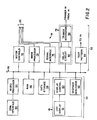
- FIG. 2 A block diagram of data processing system 16 is shown in Figure 2.
- the data processing system 16 may be divided into two broad functional groups: a computing system 50 and an electron beam test probe control system 52. Only a novel aspect of the computing system 50 will be described here.
- the basic system is described in U.S. Patent No. 4,706,019, the disclosure of which is incorporated herein by reference.
- the computing system 50 is capable of storing, processing and displaying high resolution voltage contrast images of the IC under test.
- Computer system 50 includes a microprocessor 54, a RAM memory 56, and a data storage module 58 which may comprise a disk drive.
- computer system 50 includes a display terminal 18 having a display interface 60 for driving a high resolution color display terminal 61 having a resolution of, for example, at least 1000 x 1000 pixels.
- the display terminal 18 also includes a keyboard for entering commands and a pointer means (such as a "mouse") for pointing to and specifying points on the display screen.
- Display terminal 18 may also include its own graphics generator 62 to improve the time needed to produce a graphic display.
- Computing system 50 may further include interfaces 64 for communicating with other computer systems via a communication bus 66.
- Figure 3 shows a pair of stroboscopic voltage contrast images selected from two stacks of images acquired with a Schlumberger "IDS 5000" electron beam test probe system.
- Each image is made up of an array of 512 x 512 pixels, each pixel having a digital gray-scale intensity value between 0 and 255.
- Each stack may consist of up to 100 or even more of such images. It is desired to compare two such stacks, image-by-image, pixel-by-pixel, to prepare a stack of difference images which may displayed for DFI analysis.
- the image displayed at the left side of Figure 3 has visible features (for example, those marked 1, 2, 3) which appear similar to visible features (also marked 1, 2, 3) of the image displayed at the right side of Figure 3, but the images are misaligned.
- the misalignment may be due to any of a number of factors: rotation, tilt or other differing physical orientation of the integrated circuits within the test probe, translation, display magnification, or the like. Also visible in the image at the right side of Figure 3 is a circular region, labeled 20, showing a magnified portion of the image.
- Figure 4 shows three voltage contrast images: the upper left image (in background) is the same as the upper right image of Figure 3; the upper right image (in background) is the same as the upper left image of Figure 3; and the lower center image (in foreground) is a "difference" image of the two images in background. Because of the misalignment, the difference image is of little diagnostic value.
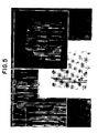
- Figure 5 also shows three voltage contrast images: the upper left image (in background) is the same as the upper left image of Figure 4; the upper right image (in foreground) is a version of the upper right image of Figure 4 which has been processed in accordance with the invention to align it with the upper left image of Figure 5; and the lower center image (in middle ground) is a "difference" image of the upper left and upper right images of Figure 5.
- the lower center image of Figure 5 makes visible the differing voltage levels (representing differing logic levels, for example) at locations within the IC devices from which the images were acquired.
- the alignment process of the present invention serves in general to "warp" one image, correcting for relative geometric distortion of the images.
- the "warped” image represents the same area of an integrated circuit as the image with which it has been aligned.
- Prior art alignment methods using floating point representation have been found to process the 512 x 512 pixels of an image to be warped in about 80 seconds, even with a dedicated floating-point math coprocessor on the same type of workstation.
- the present invention offers a method of performing the warping operation employing fixed point representations, and has been found to take about 1.3 seconds, when programmed in the "C" language on a UNIX-based Sun 3/160 workstation.
- a listing of such a program for carrying out a preferred form of the inventive method in such a workstation is included below as an Appendix to this description.
- the speed of the inventive technique allows images to be aligned quickly and interactively for use in Dynamic Fault Imaging diagnosis, without requiring a dedicated coprocessor.
- Correction of relative geometric distortions between corresponding images of two stacks may be made by first mapping the coordinate system ( x,y ) of the second image into the coordinate system ( u,v ) of the first image.
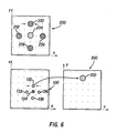
- Figure 6 shows in box 100 a grouping of features 130, 132, 134, 136, 138 which define a first image.
- the features of box 100 are formed by pixels within the graphics frame, represented by a grid of dots positioned in their ( u,v ) coordinate system.
- Box 200 shows the positions of respective corresponding features 230, 232, 234, 236, 238 of a second image in relation to the ( x,y ) coordinate system of the second image. It can be seen from comparison of the size and spacing of features 130-138 of box 100 relative to features 230-238 of box 200 that the magnification of the second image is twice (2X) that of the first image, i.e., that features of the first image are spaced half as far apart as those of the second image.
- Comparison of boxes 100 and 200 also show that the features of box 100 are positioned slightly below and to the right of the corresponding features of box 200.
- the spatial relationship of features 130, 132, 134, 136, 138 to the pixels defining them is not the same as the spatial relationship of features 230, 232, 234, 236 and 238 to the pixels defining them, it is necessary to extrapolate pixel intensity values for features 130, 132, 134, 136 and 138 at the pixel positions of the second image (box 200) in order to produce a resultant "warped" version of the first image (box 300).
- Box 300 of Figure 6 shows a feature 330 of such a resultant image, magnified and translated about 11 ⁇ 2 increments upwardly and about1 ⁇ 2 increment to the left, such that feature 330 is aligned with the position of feature 230 of the second image.
- the intensity value assigned to pixels defining feature 330 must be determined from the values of pixels from the first image, as follows.
- X and Y graphs are not available and empiric models have to be used, such as a polynomial approximation.
- One possible method of performing such mapping is described in more detail below with reference to a preferred embodiment of the invention.
- the corrected display intensity value of a given pixel p( x,y ) in the resultant graphics frame must then be extrapolated from the pixels surrounding the corresponding location of that pixel in the source graphics frame, using a convolution operation.
- the four surrounding pixels are employed and the convolution becomes a bilinear extrapolation.
- extrapolation techniques are known in the art: see, for example W. PRATT, DIGITAL IMAGE PROCESSING (1978), the disclosure of which is incorporated herein by reference, at page 115.
- Figure 7 shows in detail the relationship between location 440, which is the translated position of a pixel in the ( x,y ) coordinate system of the second image 200 to the ( u,v ) coordinate system of the first image 100, and pixels p1, p2, p3, p4 surrounding this translated position; the third dimension, p, of Figure 7 represents pixel intensity.
- the question mark ("?”) in Figure 7 represents the value of pixel 440 to be extrapolated.
- Standard convolution algorithms use floating point arithmetic or decimal variables as basic objects of computation.
- the precision of a floating point representation is the number of digits after the decimal point.
- a precision of 3 digits was discovered to be adequate for the case of a 512x512 matrix of pixels having intensity values between 0 and 255. Accordingly, the relatively slow operations with the floating point variables was avoided by replacing them with integer or "short" variables. Fixed point arithmetic operations were used, with significant savings of processing time.
- the final result is shifted by 8 (the equivalent of division by 256) to give the value of the resulting pixel.
- the present invention is preferably carried out in a series of steps, as follows:
- a cursor is moved to the location of any selected feature of the first image, a marker is placed at that location on the displayed image and the coordinate position of the feature is recorded, preferably in RAM 56.
- the cursor is moved to the location of any selected feature of the second image (preferably a feature which the operator considers to correspond to the selected feature of the first image), a marker is placed on that location of the displayed image and the coordinate position of this feature is recorded.
- the selection and recording process is then repeated for two additional features of each image.
- the amplitude of the warping operation (stretch + translation) is thereby set interactively by the user.
- computing system 50 includes a magnification feature which allows a portion of an image to be displayed in a window of selected magnification, such that individual pixels of the image may be discerned, and a capability for recording the position of a selected feature with sub-pixel precision.
- the computing system preferably permits 4X magnification of a portion of the image and placement of the cursor and recording of the cursor position with a precision of 1 ⁇ 4 to 1 ⁇ 2 pixel.
- An example of a magnified portion of an image is shown in the encircled region of the right-hand image of Figure 3.
- Such magnification aids proper alignment of images in which features, such as the width of a line representing a metal conductor in the IC device, may be defined by as few as two pixels.
- the magnification may be carried out by means of the alignment method of the present invention: the portion of the image to be magnified is treated as an image to be "warped". If the magnification is 4X, the magnified version will have 16 times as many pixels representing the same features as the selected portion of the original image. The value of each pixel in the magnified version is extrapolated from the values of the pixels surrounding the location of the original image which corresponds to the pixel of the magnified version.
- a geometric planar transformation in the form of a 3 x 3 matrix of floating point values is then calculated which maps the positions of the selected features of the first image into those of the second image.
- the three markers on the first image have the coordinates b[ i ] ⁇ x and b[ i ] ⁇ y and the three markers on the second image have the coordinates a[ i ] ⁇ x and a[ i ] ⁇ y , with i having values between 1 and 3.
- the values in the 2x2 sub-matrix M[ i ][ j ] are the factors correcting the rotation, tilt and magnification distortion of the images.
- the value of M[0][2] is the horizontal translation factor, and the value of M[1][2] is the vertical translation factor.
- an FPR is preferably an integer which is 255 times as large as the floating point variable. For instance: 0 becomes 0; 0.25 becomes 64; 0.5 becomes 127.
- An advantage of FPR transformation is that subsequent arithmetic operations to be performed will be integer operations which are many times faster to perform than floating point operations in a general-purpose processor such as microprocessor 54.
- the resultant image is then scanned line by line to transform positions of the first image into pixel positions of the resultant image, using the FPR values of the transformation matrix.
- a test is performed to determine whether a given position of the first image, when mapped into the coordinates of the resultant image, will be within the desired display field of the resultant image. It will be recalled that the intention is to have a resultant image which matches pixel-for-pixel with the second image, which has a display field of 512 lines and 512 columns of pixels. If the transformed pixel location is outside the display field, it is assigned a fixed intensity value to produce, for example a black pixel when displayed.
- the resultant image is made up of pixels, each pixel having a value that is to be calculated from the pixel values of the first image (image1).
- a location L1 in image1 (for example, location 440 in Figure 7) is transformed into a location L1a (location 330 in Figure 6) in image1-aligned.
- the pixel at the location L1a in image1-aligned retains the value extrapolated for location L1 in image1.
- FIG. 8 schematically illustrates the principle: A location a of image 1 corresponds to a location A outside the display field of image1-aligned, while a location b of image 1 corresponds to a location within the display field of image1-aligned.
- the position L1 is a decimal value. But because FPR values are used, the four tests (two for the horizontal border and two for the vertical border of the display field) may be performed with integer logical operations. The test is therefore many times faster than if done with floating point arithmetic. If the test diagnoses a pixel outside the frame of the display field, the result is set to black.
- the position L1 may be decimal (i.e., the coordinates of L1 may fall between pixels of the first image), it is necessary to extrapolate the pixel value from surrounding pixels.
- the extrapolation can be viewed as a weighted average of the four pixels surrounding position L1. If the distance between two pixels is 1 unit, the weight assigned to each pixel is 1 minus the fractional unit distance to the location.
- Pre-calculated "look-up" tables are preferably used to minimize the time needed to perform the extrapolation. Use of such tables is made possible by the use of FPR: at this stage of the alignment process it is only necessary to deal with integers that may become element numbers of a pre-calculated array of values. Instead of computing each result individually, it may simply be selected from an indexed static table of values. Such a table is preferably calculated automatically upon startup of the computing system 50, and may be stored in the active memory of RAM 56 or in "swap space" in data storage device 58. For the example given below, the table contains 2 x 65536 values, requiring about 128K bytes of storage space.
- a location of interest, L1 is surrounded by pixels, pixels P1 and p2 above, and p3 and p4 below.
- the values of these four pixels are compressed to 4 bits.
- Fixed point representations of ⁇ x and ⁇ y values ( ⁇ x and ⁇ y are decimal values between 0 and 1, as described above).
- Averaging is then performed in three steps: The average of p1 and p2 is calculated, the average of p3 and p4 is calculated, and the two averages are added.
- the first averaging makes use of the lookup table, which has 16 bit entries (representing four bits each for pixel intensity values p1 and p2, and four bits each for position values ⁇ x and ⁇ y ). The contribution of the two upper pixels is read in the lookup table.
- the index used to select the value from the lookup table is prepared by calculating decimal values between 0 and 1 for ⁇ x and ⁇ y (from the position coordinates of the location of interest L1 and the surrounding pixels), calculating a FPR for ⁇ x and ⁇ y , extracting pixel intensity values p1 and p2 and putting the four values in a single short (which is 16 bits for the UNIX-based computing system of a Schlumberger "IDS 5000" test system).
- the second averaging uses the same lookup table.
- An index which is made of p3, p4, ⁇ x and ⁇ y points in the table to a value that is the contribution of the lower pixels.
- the value of the resulting pixel (a value between 0 and 255) is the sum of the two contributions.
- the computing system 50 is capable of aligning two 512x512 pixel images with pixel intensity values of 0 to 255 in less than two seconds, if the properly indexed lookup table is pre-calculated.
- the four bits representing ⁇ x would be 8 (in decimal), the four bits representing ⁇ y would be 12, the four bits representing p1 would be 2, the four bits representing p2 would be 12, the four bits representing p3 would be 3, and the four bits representing p4 would be 13.
- the index value for the first lookup is thus 3 8 12 12, and the corresponding value from the lookup table is 42, representing the contributions of p1 and p2 to the resultant pixel.
- the index value for the second lookup is thus 3 8 13 12, and the corresponding value from the lookup table is 54, representing the contributions of p3 and p4.
- the sum of these values, 96, is the value of the resultant pixel.
- 32 gray levels pixel intensity values
- these 32 levels are represented by values ranging from 33 to 64.
- Other such modifications are possible within the spirit and scope of the present invention.
- the resultant image (a version of a first image "warped" into alignment with a second image) may be compared with the second image by subtracting intensity values, pixel-by-pixel.
- the intensity of each pixel is represented by 8 bits and thus has a value between 0 and 255.
- the difference values are between -255 and +255. Since the difference image must still be a pixel value, the -255 to 255 range must be mapped into the regular 0 to 255 gray range level.
- the difference image consists of information which falls into three ranges of intensity or bands of interest.
- the first band (from 0 to a level L1) corresponds to features that are in the second image but not in the first image.
- the second band (from L1 to a level L2) corresponds to features that are the same in both images.
- the third band (from L2 to 255) corresponds to features that are in the first image but not in the second image.
- a 3 level threshold filter is used, as illustrated in Figure 9.
- the histogram which has initially 8 bit deep gray levels (256 different grays) is mapped into a black (0 to L1), gray (L1 to L2) and white (L2 to 255) three level scale.
- a false coloring mode may be employed: instead of using images with gray levels, bright colors (i.e.: blue, yellow and red) may displayed.
- the levels may be set interactively on a selected image of the stack ("the star image"), to optimize the information, and applied to all or any desired set of images of the stack. Differences in contrast and brightness between the images of one stack (e.g., "golden device” images) and the images of the other stack (e.g., "test device” images) are addressed by just changing the threshold values.
Landscapes
- Physics & Mathematics (AREA)
- General Physics & Mathematics (AREA)
- Engineering & Computer Science (AREA)
- Theoretical Computer Science (AREA)
- Image Processing (AREA)
- Image Analysis (AREA)
- Testing Of Individual Semiconductor Devices (AREA)
- Tests Of Electronic Circuits (AREA)
- Testing Or Measuring Of Semiconductors Or The Like (AREA)
- Closed-Circuit Television Systems (AREA)
Applications Claiming Priority (2)
| Application Number | Priority Date | Filing Date | Title |
|---|---|---|---|
| US07/276,359 US5054097A (en) | 1988-11-23 | 1988-11-23 | Methods and apparatus for alignment of images |
| US276359 | 1994-07-15 |
Publications (3)
| Publication Number | Publication Date |
|---|---|
| EP0370322A2 true EP0370322A2 (de) | 1990-05-30 |
| EP0370322A3 EP0370322A3 (de) | 1991-09-25 |
| EP0370322B1 EP0370322B1 (de) | 1998-07-08 |
Family
ID=23056339
Family Applications (1)
| Application Number | Title | Priority Date | Filing Date |
|---|---|---|---|
| EP89120795A Expired - Lifetime EP0370322B1 (de) | 1988-11-23 | 1989-11-09 | Bilderausrichtungsverfahren und -gerät |
Country Status (4)
| Country | Link |
|---|---|
| US (1) | US5054097A (de) |
| EP (1) | EP0370322B1 (de) |
| JP (1) | JP2581815B2 (de) |
| DE (1) | DE68928726T2 (de) |
Cited By (9)
| Publication number | Priority date | Publication date | Assignee | Title |
|---|---|---|---|---|
| EP0790577A3 (de) * | 1995-11-27 | 1998-02-04 | Sun Microsystems, Inc. | Operationen auf Bildern |
| EP0880858A4 (de) * | 1996-02-16 | 2000-12-27 | Cornell Res Foundation Inc | Verfahren und system zur faksimilebasierten videokompression |
| WO2003088148A1 (en) * | 2002-04-05 | 2003-10-23 | General Hospital Corporation | Systems and method for generating an image |
| WO2005006731A3 (en) * | 2003-07-11 | 2005-03-03 | Axalto Sa | A method for checking the information to be printed on intermediate supports manufactured for printing an image on a final support |
| EP1955225A4 (de) * | 2005-11-18 | 2009-11-04 | Kla Tencor Tech Corp | Verfahren und systeme zur verwendung von entwurfsdaten in kombination mit prüfdaten |
| WO2009038838A3 (en) * | 2007-06-07 | 2009-11-12 | Kla-Tencor Corporation | Methods and systems for determining a position of inspection data in design data space |
| US9659670B2 (en) | 2008-07-28 | 2017-05-23 | Kla-Tencor Corp. | Computer-implemented methods, computer-readable media, and systems for classifying defects detected in a memory device area on a wafer |
| CN107533017A (zh) * | 2015-03-23 | 2018-01-02 | 泰科英赛科技有限公司 | 与成像装置中失真校正相关的方法、系统和装置 |
| US9865512B2 (en) | 2013-04-08 | 2018-01-09 | Kla-Tencor Corp. | Dynamic design attributes for wafer inspection |
Families Citing this family (69)
| Publication number | Priority date | Publication date | Assignee | Title |
|---|---|---|---|---|
| DE69227056T2 (de) * | 1991-03-22 | 1999-05-12 | Nec Corp., Tokio/Tokyo | Verfahren zur Fehleranalyse unter Verwendung eines Elektronenstrahles |
| JP3140782B2 (ja) * | 1991-12-10 | 2001-03-05 | ストーム テクノロジー,インコーポレイテッド | 画像を自動併合するための装置及び方法 |
| JP2940317B2 (ja) * | 1992-06-24 | 1999-08-25 | 三菱電機株式会社 | 画像処理装置 |
| US5748195A (en) * | 1992-10-29 | 1998-05-05 | International Business Machines Corporation | Method and means for evaluating a tetrahedral linear interpolation function |
| US5432892A (en) * | 1992-11-25 | 1995-07-11 | International Business Machines Corporation | Volummetric linear interpolation |
| US5751926A (en) * | 1992-12-23 | 1998-05-12 | International Business Machines Corporation | Function approximation using a centered cubic packing with tetragonal disphenoid extraction |
| US5390035A (en) * | 1992-12-23 | 1995-02-14 | International Business Machines Corporation | Method and means for tetrahedron/octahedron packing and tetrahedron extraction for function approximation |
| US5401972A (en) * | 1993-09-02 | 1995-03-28 | Schlumberger Technologies, Inc. | Layout overlay for FIB operations |
| US6061467A (en) * | 1994-05-02 | 2000-05-09 | Cognex Corporation | Automated optical inspection apparatus using nearest neighbor interpolation |
| IL110771A (en) * | 1994-08-25 | 1998-02-08 | Holon Holon Hanni | A priori and adaptive filtering for detection of signals corrupted by noise |
| JP3515199B2 (ja) * | 1995-01-06 | 2004-04-05 | 大日本スクリーン製造株式会社 | 欠陥検査装置 |
| US5541411A (en) * | 1995-07-06 | 1996-07-30 | Fei Company | Image-to-image registration focused ion beam system |
| US6137494A (en) * | 1995-08-18 | 2000-10-24 | International Business Machines Corporation | Method and means for evaluating a tetrahedral linear interpolation function |
| US5818951A (en) * | 1995-10-13 | 1998-10-06 | Infrared Service Corporation | Methods and related apparatus for generating thermographic survey images |
| US5917961A (en) * | 1996-10-30 | 1999-06-29 | Hewlett-Packard Co. | Image convolution using pre-calculated lookup tables |
| US6330354B1 (en) * | 1997-05-01 | 2001-12-11 | International Business Machines Corporation | Method of analyzing visual inspection image data to find defects on a device |
| US6236222B1 (en) * | 1997-11-19 | 2001-05-22 | Philips Electronics North America Corp. | Method and apparatus for detecting misalignments in interconnect structures |
| US6445399B1 (en) * | 1998-01-20 | 2002-09-03 | Rafael - Armament Development Authority Ltd. | System and method of visual orientation |
| US6115643A (en) * | 1998-02-03 | 2000-09-05 | Mcms | Real-time manufacturing process control monitoring method |
| US6690840B1 (en) | 2000-02-08 | 2004-02-10 | Tektronix, Inc. | Image alignment with global translation and linear stretch |
| EP1410004A2 (de) * | 2000-11-17 | 2004-04-21 | Molecular Diagnostics, Inc. | Auswertung von mikroskop-objektträgern |
| US7392287B2 (en) | 2001-03-27 | 2008-06-24 | Hemisphere Ii Investment Lp | Method and apparatus for sharing information using a handheld device |
| US6943569B1 (en) * | 2002-04-12 | 2005-09-13 | Advanced Micro Devices, Inc. | Method, system and apparatus to detect defects in semiconductor devices |
| JP2004021495A (ja) * | 2002-06-14 | 2004-01-22 | Mitsubishi Electric Corp | 監視システムおよび監視方法 |
| GB2405764A (en) * | 2003-09-04 | 2005-03-09 | Sharp Kk | Guided capture or selection of stereoscopic image pairs. |
| US7160741B2 (en) * | 2003-11-06 | 2007-01-09 | Chartered Semiconductor Manufacturing Ltd. | Planar voltage contrast test structure and method |
| JP4904034B2 (ja) | 2004-09-14 | 2012-03-28 | ケーエルエー−テンカー コーポレイション | レチクル・レイアウト・データを評価するための方法、システム及び搬送媒体 |
| EP1810220A4 (de) * | 2004-11-03 | 2008-04-30 | Tyzx Inc | Integrierter bildprozessor |
| US20060098897A1 (en) * | 2004-11-10 | 2006-05-11 | Agfa-Gevaert | Method of superimposing images |
| US7383994B2 (en) * | 2005-05-03 | 2008-06-10 | Datalogic Scanning, Inc. | Methods and systems for forming images of moving optical codes |
| JP4591211B2 (ja) * | 2005-05-31 | 2010-12-01 | 富士ゼロックス株式会社 | 画像処理装置、画像処理方法、媒体、符号読取装置、及びプログラム |
| US7570796B2 (en) | 2005-11-18 | 2009-08-04 | Kla-Tencor Technologies Corp. | Methods and systems for utilizing design data in combination with inspection data |
| US7676077B2 (en) | 2005-11-18 | 2010-03-09 | Kla-Tencor Technologies Corp. | Methods and systems for utilizing design data in combination with inspection data |
| US7873233B2 (en) * | 2006-10-17 | 2011-01-18 | Seiko Epson Corporation | Method and apparatus for rendering an image impinging upon a non-planar surface |
| WO2008077100A2 (en) | 2006-12-19 | 2008-06-26 | Kla-Tencor Corporation | Systems and methods for creating inspection recipes |
| WO2008086282A2 (en) | 2007-01-05 | 2008-07-17 | Kla-Tencor Corporation | Methods and systems for using electrical information for a device being fabricated on a wafer to perform one or more defect-related functions |
| US8990681B2 (en) * | 2007-01-24 | 2015-03-24 | Bluebeam Software, Inc. | Method for aligning a modified document and an original document for comparison and difference highlighting |
| US7962863B2 (en) | 2007-05-07 | 2011-06-14 | Kla-Tencor Corp. | Computer-implemented methods, systems, and computer-readable media for determining a model for predicting printability of reticle features on a wafer |
| US7738093B2 (en) | 2007-05-07 | 2010-06-15 | Kla-Tencor Corp. | Methods for detecting and classifying defects on a reticle |
| US8213704B2 (en) | 2007-05-09 | 2012-07-03 | Kla-Tencor Corp. | Methods and systems for detecting defects in a reticle design pattern |
| US7796804B2 (en) | 2007-07-20 | 2010-09-14 | Kla-Tencor Corp. | Methods for generating a standard reference die for use in a die to standard reference die inspection and methods for inspecting a wafer |
| US7711514B2 (en) | 2007-08-10 | 2010-05-04 | Kla-Tencor Technologies Corp. | Computer-implemented methods, carrier media, and systems for generating a metrology sampling plan |
| TWI469235B (zh) | 2007-08-20 | 2015-01-11 | Kla Tencor Corp | 決定實際缺陷是潛在系統性缺陷或潛在隨機缺陷之由電腦實施之方法 |
| US8139844B2 (en) | 2008-04-14 | 2012-03-20 | Kla-Tencor Corp. | Methods and systems for determining a defect criticality index for defects on wafers |
| CN102246258B (zh) | 2008-10-12 | 2015-09-02 | Fei公司 | 用于局部区域导航的高精确度射束放置 |
| US8781219B2 (en) | 2008-10-12 | 2014-07-15 | Fei Company | High accuracy beam placement for local area navigation |
| US8775101B2 (en) | 2009-02-13 | 2014-07-08 | Kla-Tencor Corp. | Detecting defects on a wafer |
| US8204297B1 (en) | 2009-02-27 | 2012-06-19 | Kla-Tencor Corp. | Methods and systems for classifying defects detected on a reticle |
| US8112241B2 (en) | 2009-03-13 | 2012-02-07 | Kla-Tencor Corp. | Methods and systems for generating an inspection process for a wafer |
| JP5683839B2 (ja) | 2010-05-17 | 2015-03-11 | セミコンダクター・コンポーネンツ・インダストリーズ・リミテッド・ライアビリティ・カンパニー | 撮像装置の制御回路 |
| US8781781B2 (en) | 2010-07-30 | 2014-07-15 | Kla-Tencor Corp. | Dynamic care areas |
| US9602697B2 (en) * | 2010-08-27 | 2017-03-21 | Ricoh Company, Ltd. | Color substitution mechanism |
| EP2612342B1 (de) | 2010-08-31 | 2018-08-22 | FEI Company | Navigation und probenbearbeitung unter verwendung einer ionenquelle mit sowohl massearmen als auch massereichen spezies |
| US9170211B2 (en) | 2011-03-25 | 2015-10-27 | Kla-Tencor Corp. | Design-based inspection using repeating structures |
| US9087367B2 (en) | 2011-09-13 | 2015-07-21 | Kla-Tencor Corp. | Determining design coordinates for wafer defects |
| US8831334B2 (en) | 2012-01-20 | 2014-09-09 | Kla-Tencor Corp. | Segmentation for wafer inspection |
| US8826200B2 (en) | 2012-05-25 | 2014-09-02 | Kla-Tencor Corp. | Alteration for wafer inspection |
| US9189844B2 (en) | 2012-10-15 | 2015-11-17 | Kla-Tencor Corp. | Detecting defects on a wafer using defect-specific information |
| US9053527B2 (en) | 2013-01-02 | 2015-06-09 | Kla-Tencor Corp. | Detecting defects on a wafer |
| US9134254B2 (en) | 2013-01-07 | 2015-09-15 | Kla-Tencor Corp. | Determining a position of inspection system output in design data space |
| US9311698B2 (en) | 2013-01-09 | 2016-04-12 | Kla-Tencor Corp. | Detecting defects on a wafer using template image matching |
| US9092846B2 (en) | 2013-02-01 | 2015-07-28 | Kla-Tencor Corp. | Detecting defects on a wafer using defect-specific and multi-channel information |
| US9310320B2 (en) | 2013-04-15 | 2016-04-12 | Kla-Tencor Corp. | Based sampling and binning for yield critical defects |
| US9265463B1 (en) | 2014-12-22 | 2016-02-23 | Medical Metrics, Inc. | Methods for determining spine instability and for eliminating the impact of patient effort on stability determinations |
| US9542732B2 (en) * | 2015-04-03 | 2017-01-10 | Cognex Corporation | Efficient image transformation |
| US10275863B2 (en) | 2015-04-03 | 2019-04-30 | Cognex Corporation | Homography rectification |
| WO2018170416A1 (en) * | 2017-03-16 | 2018-09-20 | Vid Scale, Inc. | Floating point to integer conversion for 360-degree video projection format conversion and spherical metrics calculation |
| US12190533B2 (en) * | 2020-09-14 | 2025-01-07 | The Regents Of The University Of Michigan | Focal stack camera as secure imaging device and image manipulation detection method |
| WO2022187464A1 (en) * | 2021-03-03 | 2022-09-09 | Battelle Memorial Institute | Systems and methods for inspection of ic devices |
Family Cites Families (9)
| Publication number | Priority date | Publication date | Assignee | Title |
|---|---|---|---|---|
| JPS57138685A (en) * | 1981-02-23 | 1982-08-27 | Hitachi Ltd | Graphic conversion for graphic indicator |
| US4610026A (en) * | 1982-04-30 | 1986-09-02 | Hitachi, Ltd. | Method of and apparatus for enlarging/reducing two-dimensional images |
| US4578812A (en) * | 1982-12-01 | 1986-03-25 | Nec Corporation | Digital image processing by hardware using cubic convolution interpolation |
| JPS59137942A (ja) * | 1983-01-28 | 1984-08-08 | Hitachi Ltd | 画像位置合わせ方式 |
| JPS6240146A (ja) * | 1985-08-14 | 1987-02-21 | Mitsubishi Electric Corp | 荷電ビ−ムパタ−ン欠陥検査装置 |
| US4721909A (en) * | 1985-08-16 | 1988-01-26 | Schlumberger Technology Corporation | Apparatus for pulsing electron beams |
| US4706019A (en) * | 1985-11-15 | 1987-11-10 | Fairchild Camera And Instrument Corporation | Electron beam test probe system for analyzing integrated circuits |
| US4760548A (en) * | 1986-06-13 | 1988-07-26 | International Business Machines Corporation | Method and apparatus for producing a curve image |
| US4805123B1 (en) * | 1986-07-14 | 1998-10-13 | Kla Instr Corp | Automatic photomask and reticle inspection method and apparatus including improved defect detector and alignment sub-systems |
-
1988
- 1988-11-23 US US07/276,359 patent/US5054097A/en not_active Expired - Lifetime
-
1989
- 1989-11-09 EP EP89120795A patent/EP0370322B1/de not_active Expired - Lifetime
- 1989-11-09 DE DE68928726T patent/DE68928726T2/de not_active Expired - Fee Related
- 1989-11-24 JP JP1303486A patent/JP2581815B2/ja not_active Expired - Fee Related
Cited By (13)
| Publication number | Priority date | Publication date | Assignee | Title |
|---|---|---|---|---|
| EP0790577A3 (de) * | 1995-11-27 | 1998-02-04 | Sun Microsystems, Inc. | Operationen auf Bildern |
| EP0880858A4 (de) * | 1996-02-16 | 2000-12-27 | Cornell Res Foundation Inc | Verfahren und system zur faksimilebasierten videokompression |
| WO2003088148A1 (en) * | 2002-04-05 | 2003-10-23 | General Hospital Corporation | Systems and method for generating an image |
| US7333647B2 (en) | 2002-04-05 | 2008-02-19 | The General Hospital Corporation | Systems and method for generating an image |
| WO2005006731A3 (en) * | 2003-07-11 | 2005-03-03 | Axalto Sa | A method for checking the information to be printed on intermediate supports manufactured for printing an image on a final support |
| EP1955225A4 (de) * | 2005-11-18 | 2009-11-04 | Kla Tencor Tech Corp | Verfahren und systeme zur verwendung von entwurfsdaten in kombination mit prüfdaten |
| WO2009038838A3 (en) * | 2007-06-07 | 2009-11-12 | Kla-Tencor Corporation | Methods and systems for determining a position of inspection data in design data space |
| US9659670B2 (en) | 2008-07-28 | 2017-05-23 | Kla-Tencor Corp. | Computer-implemented methods, computer-readable media, and systems for classifying defects detected in a memory device area on a wafer |
| US9865512B2 (en) | 2013-04-08 | 2018-01-09 | Kla-Tencor Corp. | Dynamic design attributes for wafer inspection |
| CN107533017A (zh) * | 2015-03-23 | 2018-01-02 | 泰科英赛科技有限公司 | 与成像装置中失真校正相关的方法、系统和装置 |
| EP3274698A4 (de) * | 2015-03-23 | 2018-12-26 | Techinsights Inc. | Verfahren, systeme und vorrichtungen im zusammenhang mit verzerrungskorrektur bei abbildungsvorrichtungen |
| US10469777B2 (en) | 2015-03-23 | 2019-11-05 | Techinsights Inc. | Methods, systems and devices relating to distortion correction in imaging devices |
| CN107533017B (zh) * | 2015-03-23 | 2021-01-08 | 泰科英赛科技有限公司 | 与成像装置中失真校正相关的方法、系统和装置 |
Also Published As
| Publication number | Publication date |
|---|---|
| DE68928726T2 (de) | 1999-04-08 |
| EP0370322B1 (de) | 1998-07-08 |
| EP0370322A3 (de) | 1991-09-25 |
| DE68928726D1 (de) | 1998-08-13 |
| JP2581815B2 (ja) | 1997-02-12 |
| JPH03162685A (ja) | 1991-07-12 |
| US5054097A (en) | 1991-10-01 |
Similar Documents
| Publication | Publication Date | Title |
|---|---|---|
| US5054097A (en) | Methods and apparatus for alignment of images | |
| EP0370323B1 (de) | Verfahren und Gerät zum Verdichten von Bildern hoher Auflösung | |
| US6757428B1 (en) | System and method for color characterization with applications in color measurement and color matching | |
| US5757198A (en) | Method and apparatus for detecting an IC defect using charged particle beam | |
| US7076101B2 (en) | Method and apparatus for local image quantification verification | |
| JPH0776974B2 (ja) | 多次元視覚解析方法及び装置 | |
| US7092571B2 (en) | Method and apparatus for regional image quantification verification | |
| US20230024820A1 (en) | Analysis device and analysis method | |
| US12254618B2 (en) | Circuit apparatus, electronic instrument, and error detection method | |
| US6961468B2 (en) | Method and apparatus for adaptive local image quantification verification | |
| Collin et al. | Device testing and SEM testing tools | |
| JP4691732B1 (ja) | 組織抽出システム | |
| US5682104A (en) | Electron beam tester and testing method using the same | |
| US6606394B1 (en) | Surface inspecting apparatus and method therefor | |
| CN108896972A (zh) | 一种基于图像识别的雷达图像仿真方法 | |
| Collin et al. | Failure analysis using e-beam | |
| Suryawan | FPGA-based geometric test pattern generator | |
| CN113870255A (zh) | Mini LED产品缺陷检测方法及相关设备 | |
| JP2645864B2 (ja) | 集積回路試験装置 | |
| EP0391587A2 (de) | Verfahren und Anordnung zur schnellen Erzeugung von Verzerrungs-Koeffizienten | |
| JP2976423B2 (ja) | 半導体集積回路の断線故障検出装置及びその方法並びにその制御プログラムを記録した記録媒体 | |
| JPH06102328A (ja) | 半導体装置の故障診断装置及びそれを用いた故障診断方法 | |
| Zeng et al. | 41‐3: A High‐Accuracy Display Compensation Method for Full‐Display with Camera | |
| JPH0321881A (ja) | Lsi診断装置 | |
| CN121544621A (zh) | 一种显示器图像的均匀性统计方法、装置及存储介质 |
Legal Events
| Date | Code | Title | Description |
|---|---|---|---|
| PUAI | Public reference made under article 153(3) epc to a published international application that has entered the european phase |
Free format text: ORIGINAL CODE: 0009012 |
|
| AK | Designated contracting states |
Kind code of ref document: A2 Designated state(s): DE FR GB IT NL |
|
| PUAL | Search report despatched |
Free format text: ORIGINAL CODE: 0009013 |
|
| AK | Designated contracting states |
Kind code of ref document: A3 Designated state(s): DE FR GB IT NL |
|
| 17P | Request for examination filed |
Effective date: 19920324 |
|
| 17Q | First examination report despatched |
Effective date: 19941114 |
|
| GRAG | Despatch of communication of intention to grant |
Free format text: ORIGINAL CODE: EPIDOS AGRA |
|
| GRAG | Despatch of communication of intention to grant |
Free format text: ORIGINAL CODE: EPIDOS AGRA |
|
| GRAG | Despatch of communication of intention to grant |
Free format text: ORIGINAL CODE: EPIDOS AGRA |
|
| GRAH | Despatch of communication of intention to grant a patent |
Free format text: ORIGINAL CODE: EPIDOS IGRA |
|
| GRAH | Despatch of communication of intention to grant a patent |
Free format text: ORIGINAL CODE: EPIDOS IGRA |
|
| GRAA | (expected) grant |
Free format text: ORIGINAL CODE: 0009210 |
|
| AK | Designated contracting states |
Kind code of ref document: B1 Designated state(s): DE FR GB IT NL |
|
| PG25 | Lapsed in a contracting state [announced via postgrant information from national office to epo] |
Ref country code: IT Free format text: LAPSE BECAUSE OF FAILURE TO SUBMIT A TRANSLATION OF THE DESCRIPTION OR TO PAY THE FEE WITHIN THE PRE;WARNING: LAPSES OF ITALIAN PATENTS WITH EFFECTIVE DATE BEFORE 2007 MAY HAVE OCCURRED AT ANY TIME BEFORE 2007. THE CORRECT EFFECTIVE DATE MAY BE DIFFERENT FROM THE ONE RECORDED.SCRIBED TIME-LIMIT Effective date: 19980708 |
|
| REF | Corresponds to: |
Ref document number: 68928726 Country of ref document: DE Date of ref document: 19980813 |
|
| PGFP | Annual fee paid to national office [announced via postgrant information from national office to epo] |
Ref country code: GB Payment date: 19980930 Year of fee payment: 10 |
|
| ET | Fr: translation filed | ||
| PLBE | No opposition filed within time limit |
Free format text: ORIGINAL CODE: 0009261 |
|
| STAA | Information on the status of an ep patent application or granted ep patent |
Free format text: STATUS: NO OPPOSITION FILED WITHIN TIME LIMIT |
|
| 26N | No opposition filed | ||
| PGFP | Annual fee paid to national office [announced via postgrant information from national office to epo] |
Ref country code: NL Payment date: 19991027 Year of fee payment: 11 |
|
| PG25 | Lapsed in a contracting state [announced via postgrant information from national office to epo] |
Ref country code: GB Free format text: LAPSE BECAUSE OF NON-PAYMENT OF DUE FEES Effective date: 19991109 |
|
| PG25 | Lapsed in a contracting state [announced via postgrant information from national office to epo] |
Ref country code: NL Free format text: LAPSE BECAUSE OF NON-PAYMENT OF DUE FEES Effective date: 20000601 |
|
| GBPC | Gb: european patent ceased through non-payment of renewal fee |
Effective date: 19991109 |
|
| NLV4 | Nl: lapsed or anulled due to non-payment of the annual fee |
Effective date: 20000601 |
|
| PGFP | Annual fee paid to national office [announced via postgrant information from national office to epo] |
Ref country code: DE Payment date: 20021114 Year of fee payment: 14 |
|
| PG25 | Lapsed in a contracting state [announced via postgrant information from national office to epo] |
Ref country code: DE Free format text: LAPSE BECAUSE OF NON-PAYMENT OF DUE FEES Effective date: 20040602 |
|
| PGFP | Annual fee paid to national office [announced via postgrant information from national office to epo] |
Ref country code: FR Payment date: 20041105 Year of fee payment: 16 |
|
| PG25 | Lapsed in a contracting state [announced via postgrant information from national office to epo] |
Ref country code: FR Free format text: LAPSE BECAUSE OF NON-PAYMENT OF DUE FEES Effective date: 20060731 |
|
| REG | Reference to a national code |
Ref country code: FR Ref legal event code: ST Effective date: 20060731 |