EP0370421A1 - Absorber für elektromagnetische Wellen - Google Patents
Absorber für elektromagnetische Wellen Download PDFInfo
- Publication number
- EP0370421A1 EP0370421A1 EP89121399A EP89121399A EP0370421A1 EP 0370421 A1 EP0370421 A1 EP 0370421A1 EP 89121399 A EP89121399 A EP 89121399A EP 89121399 A EP89121399 A EP 89121399A EP 0370421 A1 EP0370421 A1 EP 0370421A1
- Authority
- EP
- European Patent Office
- Prior art keywords
- electromagnetic wave
- wave absorbing
- wave absorber
- absorbing layers
- electromagnetic
- Prior art date
- Legal status (The legal status is an assumption and is not a legal conclusion. Google has not performed a legal analysis and makes no representation as to the accuracy of the status listed.)
- Withdrawn
Links
- 239000006096 absorbing agent Substances 0.000 title claims abstract description 88
- OKTJSMMVPCPJKN-UHFFFAOYSA-N Carbon Chemical compound [C] OKTJSMMVPCPJKN-UHFFFAOYSA-N 0.000 claims abstract description 27
- 229910052799 carbon Inorganic materials 0.000 claims abstract description 27
- 239000000463 material Substances 0.000 claims abstract description 23
- 239000011347 resin Substances 0.000 claims abstract description 23
- 229920005989 resin Polymers 0.000 claims abstract description 23
- 230000000644 propagated effect Effects 0.000 claims abstract description 4
- 230000010287 polarization Effects 0.000 claims description 11
- 239000007787 solid Substances 0.000 claims description 5
- 238000003475 lamination Methods 0.000 claims description 3
- 230000004308 accommodation Effects 0.000 claims 4
- 230000005540 biological transmission Effects 0.000 claims 4
- 239000011810 insulating material Substances 0.000 claims 2
- 230000005855 radiation Effects 0.000 claims 2
- 241000490025 Schefflera digitata Species 0.000 claims 1
- 235000015250 liver sausages Nutrition 0.000 claims 1
- 239000004576 sand Substances 0.000 claims 1
- 239000002245 particle Substances 0.000 description 7
- 239000011358 absorbing material Substances 0.000 description 6
- 230000002238 attenuated effect Effects 0.000 description 5
- 239000002184 metal Substances 0.000 description 5
- 238000010521 absorption reaction Methods 0.000 description 4
- 238000002310 reflectometry Methods 0.000 description 4
- 238000012986 modification Methods 0.000 description 3
- 230000004048 modification Effects 0.000 description 3
- 230000000694 effects Effects 0.000 description 2
- 238000002474 experimental method Methods 0.000 description 2
- 239000012212 insulator Substances 0.000 description 2
- 238000005259 measurement Methods 0.000 description 2
- JOYRKODLDBILNP-UHFFFAOYSA-N Ethyl urethane Chemical compound CCOC(N)=O JOYRKODLDBILNP-UHFFFAOYSA-N 0.000 description 1
- PPBRXRYQALVLMV-UHFFFAOYSA-N Styrene Chemical compound C=CC1=CC=CC=C1 PPBRXRYQALVLMV-UHFFFAOYSA-N 0.000 description 1
- BZHJMEDXRYGGRV-UHFFFAOYSA-N Vinyl chloride Chemical compound ClC=C BZHJMEDXRYGGRV-UHFFFAOYSA-N 0.000 description 1
- 230000001154 acute effect Effects 0.000 description 1
- 230000003444 anaesthetic effect Effects 0.000 description 1
- 238000006243 chemical reaction Methods 0.000 description 1
- 239000004020 conductor Substances 0.000 description 1
- 230000001678 irradiating effect Effects 0.000 description 1
- 229920002635 polyurethane Polymers 0.000 description 1
- 239000004814 polyurethane Substances 0.000 description 1
- 239000013585 weight reducing agent Substances 0.000 description 1
Images





Classifications
-
- H—ELECTRICITY
- H01—ELECTRIC ELEMENTS
- H01Q—ANTENNAS, i.e. RADIO AERIALS
- H01Q17/00—Devices for absorbing waves radiated from an antenna; Combinations of such devices with active antenna elements or systems
- H01Q17/007—Devices for absorbing waves radiated from an antenna; Combinations of such devices with active antenna elements or systems with means for controlling the absorption
-
- G—PHYSICS
- G01—MEASURING; TESTING
- G01R—MEASURING ELECTRIC VARIABLES; MEASURING MAGNETIC VARIABLES
- G01R29/00—Arrangements for measuring or indicating electric quantities not covered by groups G01R19/00 - G01R27/00
- G01R29/08—Measuring electromagnetic field characteristics
- G01R29/10—Radiation diagrams of antennas
- G01R29/105—Radiation diagrams of antennas using anechoic chambers; Chambers or open field sites used therefor
-
- H—ELECTRICITY
- H01—ELECTRIC ELEMENTS
- H01Q—ANTENNAS, i.e. RADIO AERIALS
- H01Q17/00—Devices for absorbing waves radiated from an antenna; Combinations of such devices with active antenna elements or systems
Definitions
- This invention relates to an electromagnetic wave absorber used for anechoic or semi-anechoic chambers or shield rooms.
- Anechoic or semi-anechoic chambers are used for measuring electromagnetic wave noises generated from various electronic devices represented by computers without receiving influence of external electromagnetic waves.
- Such an anechoic chamber is constituted by a space covered by metal shield walls for preventing intrusion of external electromagnetic waves.
- an electromagnetic wave noise source and a receiving unit for measuring noise are disposed in the space for determining the state of noise generation in a state free from external electromagnetic waves.
- electromagnetic wave absorber is applied to its shield wall inner surface.
- An anechoic chamber using electromagnetic wave absorber applied to it is disclosed in, for instance, Japanese Patent Laid-Open Sho 61(1986)-292,999.
- the electromagnetic wave absorber is used those of resistive type.
- This type of electromagnetic wave absorber is of pyramid type. The sectional area of resistor is increased in relation to the progress of electromagnetic waves, and electromagnetic energy of electromagnetic waves striking the resistor is converted into thermal energy to avoid reflection of electromagnetic waves.
- the prior art electromagnetic wave absorber has a pyramidal shape so that its sectional area increases in relation to the progress of electromagnetic waves. This is done so because with the smaller sectional area of the surface section of the electromagnetic wave absorber the electric conductivity and dielectric constant of that section is the lower so that it is possible to avoid reflection of incident waves and the greater the electric conductivity and dielectric constant the greater is the energy loss, i.e., conversion of electromagnetic energy into thermal energy in the partient part of the absorber.
- the weight of the electromagnetic wave absorber is increased to present the above problems.
- the inventors have conducted various experiments in order to develop electromagnetic wave absorbers, which are light in weight and can reliably absorb electromagnetic waves in a wide frequency range of 30MHz to 1 GHz in an anechoic chamber.
- a plurality of electromagnetic wave absorbing plates are disposed side by side at a prescribed interval, and electromagnetic waves are passed through these plates to cause their energy loss, while suppressing their reflection by plates nearer an electromagnetic wave source and cause their great absorption by remoter plates.
- the absorption of waves is increased, the reflection of waves toward the wave source in the pertinent portion is increased.
- waves returning from positions remoter from the wave source are transmitted through electromagnetic wave absorber plates even when the waves are reflected waves.
- the inventor further endeavored to obtain a structure which can cause energy loss and absorb waves. If there is such a structure, it will permit reliable absorption of incident waves to suppress reflection thereof without increasing the weight of the electromagnetic wave absorber.
- Electromagnetic wave at various frequencies are irradiated on an electromagnetic wave absorbing plate having a certain thickness to find that waves at frequencies below 200 MHz are comparatively readily transmitted through the plate while waves at higher frequencies are comparatively difficulty transmitted to result in comparatively great loss while they are being transmitted through the plate.
- An experiment is also conducted with respect to waves at the above frequencies using an electromagnetic waves absorbing plate having an increased thickness to find that high frequency waves behave with respect to the increased thickness plate as though the electric conductivity and dielectric constant were increased and reflected by an increased amount by the plate surface while low frequency waves are losses by an increased amount in the plate.
- a primary object of the invention is to provide an electromagnetic wave absorber comprising a hollow taper section consisting of a pyramidal shell formed by electromagnetic wave absorbing plates containing carbon particles and a stem section provided on the bottom of the taper section and including a plurality of electromagnetic wave absorbing plates containing carbon particles, the electromagnetic wave absorbing plates having different thicknesses and arranged at a prescribed interval from one another in the stem section.
- Another object of the invention is to provide an electromagnetic wave absorber, which can suppress reflection of electromagnetic waves over a frequency range from low frequencies of about 30 MHz to high frequencies of several GHz.
- a further object of the invention is to provide an electromagnetic wave absorber, wherein the electromagnetic wave absorbing plates disposed in the stem section have progressively greater thicknesses as one goes away from the taper section.
- a still further object of the invention is to provide an electromagnetic wave absorbing material, in which electromagnetic wave absorbing plates having the same thickness are used to form the taper section and disposed in the stem section, and different numbers of electromagnetic wave absorbing plates are provided in the stem section as different laminations arranged at a prescribed interval from one another.
- a yet further object of the invention is to provide an electromagnetic wave absorber, in which the electromagnetic wave absorbing plates each have a lightweight structure having a plurality of distinct strip-like inner spaces.
- an electromagnetic wave absorber for converting energy of propagated electromagnetic waves into heat energy for absorbing the electromagnetic waves, comprising: a hollow taper section consisting of a shell formed by plates composed of a resin as base material and incorporating carbon; a stem section bounded to the bottom of the taper section; and a plurality of electromagnetic wave absorbing layers disposed internally at a prescribed interval from one another and extending in a direction substantially at right angles to the center line of the taper section, the electromagnetic wave absorbing layers consisting of plates composed of a resin as base material and incorporating carbon; the electromagnetic wave absorbing layers increasing stepwise in thickness as the layer goes away from the taper section, so that the average electric conductivity of a region in the stem section extending in the right angle direction increases stepwise as the region goes away from the taper section.
- Fig. 1 shows an embodiment of electromagnetic wave absorber 1 according to the invention.
- the electromagnetic wave absorber 1 comprises a taper section 2 which is also called right pyramid section or cone section and a rectangular stem section 3 integral with the bottom of the taper section 2.
- the taper section 2 is hollow and consists of electromagnetic wave absorbing plates 10.
- the electromagnetic wave absorbing plate 10 consists of inner and outer walls 11 and 12 spaced apart by a prescribed interval and plurality of parallel connecting walls 13 extending at right angle to and connecting together inner and outer walls 11 and 12. A plurality of strip-like spaces are thus defined in the electromagnetic wave absorbing plates 10.
- Walls 11 to 13 are made of a material composed of polypropyrene and incorporating carbon particles, and they have a thickness of about 1 to several millimeters. They are electric conductors having a resistance of 103 to 104 ohms, for instance, which is determined by the amount of carbon particles incorporated. Their dielectric constant is set to a given value by adjusting the amount of carbon.
- the stem section 3 includes five stationary layers 15a to 15b, which are made of a foamed resin such as foamed styrol or foamed urethane, i.e., an insulator, and form electromagnetic space or "null", and four electromagnetic wave absorbing layers 16a to 16d, which intervene between adjacent ones of stationary layers 15a to 15e and has the same structure as electromagnetic wave absorbing plates 10.
- the electromagnetic wave absorbing layers inclusive of the stationary layers consisting of insulator the average electric conductivity of a zone extending in a direction at right angle to the center axis of the electromagnetic wave absorber is increased stepwise as one goes away from the taper section 2.
- the first electromagnetic wave absorbing layer 16a which is nearest to the taper section 2, as shown in Fig. 4A, consists of an electromagnetic wave absorbing plate 10a having the plate 10, consisting of upper and lower walls 11a and 12a and a plurality of connecting walls 13a connecting together walls 11a and 12a. Again it is made of a material composed of polypropyrene and incorporating carbon particles.
- the second electromagnetic wave absorbing layer 16b is located to be remoter from taper section 2 than the layer 16a. As shown in Fig. 4B, it consists of two electromagnetic wave absorbing plates 10b1 and 10b2. Like electromagnetic wave absorbing plate 10a, plate 10b1 consists of upper an lower walls 11b1 and 12b1 and connecting walls 13b1 while plate 10b2 consists of upper and lower walls 11b2 and 12b2 and connecting walls 13b2.
- the third and fourth electromagnetic wave absorbing layers 16c and 16d as shown in Figs. 4C and 4D, respectively consist of three and four electromagnetic wave absorbing plates same as that of the first electromagnetic wave absorbing layer.
- the fourth electromagnetic wave absorbing layer 16d is the final layer.
- the electromagnetic wave absorbing plates constituting the electromagnetic wave absorbing layers are hollow and light in weight.
- Figs. 5A and 5B show the single electromagnetic wave absorber 1 mounted in an anechoic chamber, exaggeratingly.
- the anechoic chamber 20 has an inner measuring space 27 which is rectangular in a horizontal plane, and defined by metal walls. i.e., side walls 21 to 24, a ceiling wall 25 and a bottom wall 26, these walls preventing intrusion of external electromagnetic waves into the space 27.
- anechoic chamber 20 is provided with an operator's entrance/exit and a measuring instrument entrance/exit. In Figs. 5A and 5B such entrances/exits are not shown.
- a transmitter 28 for transmitting electromagnetic waves and a receiving antenna 29 for receiving linearly polarized components of the transmitted waves are disposed.
- the transmitter 28 transmits waves having vertically polarization components
- the receiving antenna 29 uses a rod-like linearly polarization component antenna.
- a horizontally extending receiving antenna 29 is disposed, as shown by phantom lines in Fig. 5B.
- the primary reflected wave the receiving antenna 29 is reached at obtuser angles to the left and right walls 23 and 24 than to the front and rear walls 21 and 22.
- the obtuse the reflection angle the greater is the amount of primary reflected waves incident on the receiving antenna 29.
- electromagnetic wave absorber 1 is mounted on the inner surface of either one of walls 21 to 24 such that the connecting walls 13a of the first electromagnetic wave absorbing layer 16a are directed horizontally.
- vertically polarization components of waves transmitted from transmitter 28 are mainly reflected by left and right walls 23 and 24 and reach receiving antenna 29.
- a greater portion of wave is transmitted through the connecting walls 13a of the first electromagnetic wave absorbing layer 16a, and the reflection is reduced.
- a comparatively small amount of wave reaches receiving antenna 29 after reflection by the front and rear walls 21 and 22 because wave from the transmitter 28 is incident on walls 21 and 22 at an acute angle.
- electromagnetic wave absorber 1 when it is considered to mount electromagnetic wave absorber 1 on the inner surface of the upper and lower walls 25 and 26, it is desired to mount the material 1 such that the connecting walls 13a of first electromagnetic wave absorbing layer 16a are directed in the longitudinal direction of anechoic chamber 20, i.e., the direction of line connecting transmitter 28 and receiving antenna 29.
- all the connecting walls may be directed in the same direction.
- electromagnetic wave absorber 1 When electromagnetic wave absorber 1 according to the invention is mounted in the anechoic chamber 20 as shown in Figs. 5A and 5B, waves from transmitter 28 are incident on the taper section 2 of the electromagnetic wave absorber 1. Since the taper section 2 has inclined surfaces, less primary reflected waves therefrom directly reach the receiving antenna 29. Also, wave is readily transmitted through comparatively thin electromagnetic wave absorbing plate 10. Further, since the plate 10 is inclined, a function as if there were a thicker electromagnetic wave absorbing material than the plate 10 is provided for an incident wave parallel to the center line of electromagnetic wave absorber 1.
- Wave transmitted through the taper section 2 is attenuated to be incident on the first electromagnetic wave absorbing layer 16a.
- the transmitted and attenuated wave is further transmitted through the subsequent layers to each fourth layer 16d.
- the material lying in a lateral plane transmits a comparatively large amount of wave because of the low density, thus increasing the amount of wave captured in the stem section 3.
- the captured wave partly emerges from the electromagnetic wave absorber 1 and reflected toward the space 27 to be further attenuated by electromagnetic wave absorbing plates, through which the wave has already been transmitted.
- electromagnetic wave absorbing plates having the same electric conductivity provides higher transmissivity to incident waves at low frequencies of about 30 to 200 MHz than to waves at higher frequencies.
- the thickness of the first to fourth layer 16a to 16d is increased by one electromagnetic wave absorbing plate for each layer toward the fourth layer 16d.
- the average electric conductivity is increased stepwise for region including each layer, and transmissvity is progressively reduced with low frequency waves as well.
- incident waves strike the electromagnetic wave absorbing layers stepwise to increase attenuation.
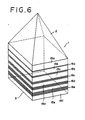
- Fig. 6 shows a different embodiment of electromagnetic wave absorber 1 according to the invention.
- the stem section 3 has five electromagnetic wave absorbing layers 16a to 16e and six stationary layers 15a to 15f made of a resin.
- each electromagnetic wave absorbing plate was hollow as shown in Figs. 3 and 4A to 4D.
- solid electromagnetic wave absorbing plates as shown in Fig. 7.
- first layer 16a is constituted by a single electromagnetic wave absorbing plate made of a resin containing carbon particles, and the succeeding layers increasing numbers of plates by one for each layer.
- Fig. 8 shows a further embodiment of electromagnetic wave absorber according to the invention.
- the electromagnetic wave absorber 1 shown in Fig. 1 is covered by a cover 30 several centimeters thick.
- the cover 30 desirably uses a foamed resin like the stationary layers for weight reduction. In the illustrated case, foamed polyurethane is used.
- the cover 30 desirably contains carbon particles as noted above, and in this case electromagnetic wave absorption effect can be obtained with the cover 30 itself as well.
- Fig. 9 is a sectional view showing a further embodiment of the electromagnetic wave absorber according to the invention.
- the stem section 3 integral with the bottom of the taper section 2 has a shape as an extension of the taper of the taper section 2.
- the outer walls of the stem section 3 are extensions of the walls of the taper section 2.
- These walls may be constituted by hollow electromagnetic wave absorbing plates as those shown in Fig. 2. In the illustrated case, however, they are constituted by solid electromagnetic wave absorbing materials.
- the stem section 3 has four electromagnetic wave absorbing layers 41 to 44 spaced apart from one another, i.e., defining a space between adjacent ones of these layers.
- the first electromagnetic wave absorbing layer 41 is constituted by a single electromagnetic wave absorbing plate, and the individual layers have increasing numbers of layers by one for each other toward the fourth layer 44.
- Fig. 10 shows a further embodiment of electromagnetic wave absorber according to the invention.
- the basic structure in this case is almost the same as the electromagnetic wave absorber shown in Fig. 9.
- ten electromagnetic wave absorbing plates 51a to 51j are incorporated in the stem section 3. These plates are spaced apart from one another such that the distance between adjacent ones of them is reduced as one goes away from the taper section 2.
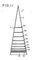
- Fig. 11 shows a modification of electromagnetic wave absorber shown in Fig. 10.
- the same number of electromagnetic wave absorbing plates 51a to 51j are used.
- the modification is different from the structure shown in Fig. 10 in that the steam section 3 has a greater height than the height of the taper section 2.
- resin to which carbon is added may be used various resins such as vinyl chloride as well as polypropyrene noted above.
- Figs. 12A and 12B are graphs showing measurement date concerning the electromagnetic wave absorbing effect according to the invention.
- Fig. 12A shows measurement data concerning the reflectivity of electromagnetic wave absorber only, without use of metal plates corresponding to wall members constituting an anechoic chamber.
- Data labeled A is of the reflectivity of an electromagnetic wave absorber including taper section 2 also called cone section and stem section 3 as showing in Fig. 1
- data labeled B is of the reflectivity of an electromagnetic wave absorber consisting of taper section 2 only.
- Fig. 12B shows data obtained by mounting electromagnetic wave absorber on metal reflecting plates corresponding to wall members constituting an anechoic chamber, irradiating the electromagnetic wave absorber with wave and measuring the reflectivity of the electramagnetic wave absorber.
- date labeled A is obtained with the electromagnetic wave absorber including the taper section 2 and stem section 3
- data labeled B is obtained with the electromagnetic wave absorber consisting of taper section 2 only.
- the reflectively can obviously be reduced over a wide frequency range from low to high frequencies.
- taper section in the illustrated embodiments is pyramidal, it is possible to use a conical taper section as well.
- incident high frequency electromagnetic waves are captured in the stem section with their reflection suppressed by electromagnetic wave absorbing layers near the taper section.
- incident low frequency waves are attenuated till reaching the final layer, which has increased electric conductivity, although they intrude up to a layer near the final layer.
- each electromagnetic wave absorbing layer waves reflected by each electromagnetic wave absorbing layer are attenuated in each region, through which they have been transmitted, thus greatly reducing the amount of wave returning to the space in the anechoic chamber after reflection.
- the taper section of the electromagnetic wave absorber is constituted by electromagnetic wave absorbing material which is hollow and light in weight, the electromagnetic wave absorber can be readily mounted in the anechoic chamber. In addition, the electromagnetic wave absorber can reliably capture waves particularly in a low frequency region and eliminate reflection.
Landscapes
- Physics & Mathematics (AREA)
- Electromagnetism (AREA)
- General Physics & Mathematics (AREA)
- Shielding Devices Or Components To Electric Or Magnetic Fields (AREA)
- Aerials With Secondary Devices (AREA)
Applications Claiming Priority (2)
| Application Number | Priority Date | Filing Date | Title |
|---|---|---|---|
| JP63295493A JPH02142200A (ja) | 1988-11-22 | 1988-11-22 | 電波吸収体 |
| JP295493/88 | 1988-11-22 |
Publications (1)
| Publication Number | Publication Date |
|---|---|
| EP0370421A1 true EP0370421A1 (de) | 1990-05-30 |
Family
ID=17821323
Family Applications (1)
| Application Number | Title | Priority Date | Filing Date |
|---|---|---|---|
| EP89121399A Withdrawn EP0370421A1 (de) | 1988-11-22 | 1989-11-18 | Absorber für elektromagnetische Wellen |
Country Status (3)
| Country | Link |
|---|---|
| EP (1) | EP0370421A1 (de) |
| JP (1) | JPH02142200A (de) |
| KR (1) | KR900008719A (de) |
Cited By (8)
| Publication number | Priority date | Publication date | Assignee | Title |
|---|---|---|---|---|
| EP0584011A1 (de) * | 1992-08-18 | 1994-02-23 | TDK Corporation | Absorber für elektromagnetische Wellen und Wellenabsorbierkonstruktion |
| WO1995000983A1 (de) * | 1993-06-25 | 1995-01-05 | Nimtz Guenter | Anordnung zur absorption von elektromagnetischen wellen und verfahren zur herstellung dieser anordnung |
| FR2710459A1 (fr) * | 1993-09-21 | 1995-03-31 | Ibm | Absorbeur avec réflexion basse optimisée. |
| EP0689262A1 (de) * | 1994-06-23 | 1995-12-27 | Takenaka Corporation | Wellenabsorbierende Zusammensetzung, Absorberelement für Funkwellen, Funkwellenabsorber und Verfahren zur Herstellung von Absorberelementen |
| EP0689263A1 (de) * | 1994-06-21 | 1995-12-27 | SIBET Gmbh SICAN FORSCHUNGS- UND ENTWICKLUNGSBETRIEBSGESELLSCHAFT mbH | Absorber für Einrichtungen zur Ermittlung der elektromagnetischen Verträglichkeit elektrischer und elektronischer Systeme |
| FR2772520A1 (fr) * | 1997-12-11 | 1999-06-18 | Giat Ind Sa | Materiau composite structural absorbant les ondes radar et utilisation d'un tel materiau |
| GB2434251A (en) * | 2006-01-16 | 2007-07-18 | Univ Sheffield | Absorber |
| CN102995863A (zh) * | 2012-12-26 | 2013-03-27 | 东南大学 | 薄型复合多层带隙微波暗室墙体衬里 |
Families Citing this family (6)
| Publication number | Priority date | Publication date | Assignee | Title |
|---|---|---|---|---|
| JP5422343B2 (ja) * | 2009-11-16 | 2014-02-19 | Necトーキン株式会社 | 複合型中空電波吸収体及びそれを用いた電波吸収壁、電波暗室 |
| JP5488620B2 (ja) * | 2010-02-15 | 2014-05-14 | 日本電気株式会社 | 電波吸収体、及びパラボラアンテナ |
| KR102258919B1 (ko) * | 2018-01-30 | 2021-06-02 | 엘지이노텍 주식회사 | 차폐층을 포함하는 안테나 모듈 및 무선 전력 수신 장치 |
| KR101971091B1 (ko) | 2018-01-30 | 2019-04-22 | 엘지이노텍 주식회사 | 차폐층을 포함하는 안테나 모듈 및 무선 전력 수신 장치 |
| CN108901194B (zh) * | 2018-08-14 | 2024-07-23 | 桂林电子科技大学 | 一种新型超宽带吸波器 |
| JP7410708B2 (ja) * | 2019-12-24 | 2024-01-10 | 株式会社アドバンテスト | 電子部品試験装置、ソケット、及び、電子部品試験装置用の交換部品 |
Citations (5)
| Publication number | Priority date | Publication date | Assignee | Title |
|---|---|---|---|---|
| US3234549A (en) * | 1961-03-20 | 1966-02-08 | Mcmillan Corp Of North Carolin | Absorber for radio waves |
| US3836967A (en) * | 1958-03-10 | 1974-09-17 | R Wright | Broadband microwave energy absorptive structure |
| US4170010A (en) * | 1968-03-04 | 1979-10-02 | Rockwell International Corporation | Inflatable radiation attenuator |
| US4381510A (en) * | 1981-08-18 | 1983-04-26 | The Boeing Co. | Microwave absorber |
| FR2610780A1 (fr) * | 1987-02-07 | 1988-08-12 | Rheinhold & Mahla Gmbh | Absorbeur pour des rayonnements electromagnetiques |
-
1988
- 1988-11-22 JP JP63295493A patent/JPH02142200A/ja active Pending
-
1989
- 1989-11-18 EP EP89121399A patent/EP0370421A1/de not_active Withdrawn
- 1989-11-22 KR KR1019890016978A patent/KR900008719A/ko not_active Ceased
Patent Citations (5)
| Publication number | Priority date | Publication date | Assignee | Title |
|---|---|---|---|---|
| US3836967A (en) * | 1958-03-10 | 1974-09-17 | R Wright | Broadband microwave energy absorptive structure |
| US3234549A (en) * | 1961-03-20 | 1966-02-08 | Mcmillan Corp Of North Carolin | Absorber for radio waves |
| US4170010A (en) * | 1968-03-04 | 1979-10-02 | Rockwell International Corporation | Inflatable radiation attenuator |
| US4381510A (en) * | 1981-08-18 | 1983-04-26 | The Boeing Co. | Microwave absorber |
| FR2610780A1 (fr) * | 1987-02-07 | 1988-08-12 | Rheinhold & Mahla Gmbh | Absorbeur pour des rayonnements electromagnetiques |
Non-Patent Citations (1)
| Title |
|---|
| ELECTRONICS AND COMMUNICATIONS IN JAPAN * |
Cited By (12)
| Publication number | Priority date | Publication date | Assignee | Title |
|---|---|---|---|---|
| EP0584011A1 (de) * | 1992-08-18 | 1994-02-23 | TDK Corporation | Absorber für elektromagnetische Wellen und Wellenabsorbierkonstruktion |
| US5373296A (en) * | 1992-08-18 | 1994-12-13 | Tdk Corporation | Electromagnetic wave absorber and wave absorption structure |
| WO1995000983A1 (de) * | 1993-06-25 | 1995-01-05 | Nimtz Guenter | Anordnung zur absorption von elektromagnetischen wellen und verfahren zur herstellung dieser anordnung |
| FR2710459A1 (fr) * | 1993-09-21 | 1995-03-31 | Ibm | Absorbeur avec réflexion basse optimisée. |
| EP0689263A1 (de) * | 1994-06-21 | 1995-12-27 | SIBET Gmbh SICAN FORSCHUNGS- UND ENTWICKLUNGSBETRIEBSGESELLSCHAFT mbH | Absorber für Einrichtungen zur Ermittlung der elektromagnetischen Verträglichkeit elektrischer und elektronischer Systeme |
| EP0689262A1 (de) * | 1994-06-23 | 1995-12-27 | Takenaka Corporation | Wellenabsorbierende Zusammensetzung, Absorberelement für Funkwellen, Funkwellenabsorber und Verfahren zur Herstellung von Absorberelementen |
| US5932054A (en) * | 1994-06-23 | 1999-08-03 | Takenaka Corporation | Radio wave absorber composition, radio wave absorber member, radio wave absorber, and method for producing radio wave absorber member |
| FR2772520A1 (fr) * | 1997-12-11 | 1999-06-18 | Giat Ind Sa | Materiau composite structural absorbant les ondes radar et utilisation d'un tel materiau |
| EP0924798A1 (de) * | 1997-12-11 | 1999-06-23 | Giat Industries | Radarabsorbierendes Verbundmaterial und dessen Verwendung |
| US6111534A (en) * | 1997-12-11 | 2000-08-29 | Giat Industries | Structural composite material absorbing radar waves and use of such a material |
| GB2434251A (en) * | 2006-01-16 | 2007-07-18 | Univ Sheffield | Absorber |
| CN102995863A (zh) * | 2012-12-26 | 2013-03-27 | 东南大学 | 薄型复合多层带隙微波暗室墙体衬里 |
Also Published As
| Publication number | Publication date |
|---|---|
| JPH02142200A (ja) | 1990-05-31 |
| KR900008719A (ko) | 1990-06-04 |
Similar Documents
| Publication | Publication Date | Title |
|---|---|---|
| Sievenpiper et al. | High-impedance electromagnetic surfaces with a forbidden frequency band | |
| US5583318A (en) | Multi-layer shield for absorption of electromagnetic energy | |
| US5103241A (en) | High Q bandpass structure for the selective transmission and reflection of high frequency radio signals | |
| US20040206527A1 (en) | Frequency-selective shield structure and electric device having the structure | |
| US5095311A (en) | Electromagnetic wave absorbing element | |
| JPH02142200A (ja) | 電波吸収体 | |
| US4381510A (en) | Microwave absorber | |
| EP0327675A2 (de) | Abschirmungsmembran | |
| US6359581B2 (en) | Electromagnetic wave abosrber | |
| JP2001156487A (ja) | 電波吸収体及びその製造方法 | |
| US8643530B2 (en) | Apparatus for radar target cloaking using polyhedral conducting mesh | |
| US4480256A (en) | Microwave absorber | |
| KR102119723B1 (ko) | 복합재 레이어와 이를 포함하는 구조 일체형 연료 탱크 및 항공기 | |
| US5358787A (en) | RF absorptive window | |
| JP3435916B2 (ja) | フェーズドアレーアンテナ装置 | |
| Itou et al. | A fundamental study of a thin λ/4 wave absorber using FSS technology | |
| US5642118A (en) | Apparatus for dissipating electromagnetic waves | |
| US5617096A (en) | Broad-band radio wave absorber | |
| EP1195848B1 (de) | Mikrowellenabsorberwand | |
| CN117080713B (zh) | 一种基于辐散一体化的相控阵天线平台 | |
| US3365667A (en) | Shielded chamber for measuring electromagnetic or acoustic waves | |
| JPH0241197B2 (ja) | Denpamukyoshitsu | |
| JPH04140905A (ja) | 平面アンテナ | |
| JP7847811B2 (ja) | 電波吸収体およびアンテナ | |
| US3680133A (en) | Subsurface traveling wave antenna |
Legal Events
| Date | Code | Title | Description |
|---|---|---|---|
| PUAI | Public reference made under article 153(3) epc to a published international application that has entered the european phase |
Free format text: ORIGINAL CODE: 0009012 |
|
| AK | Designated contracting states |
Kind code of ref document: A1 Designated state(s): DE FR GB NL |
|
| 17P | Request for examination filed |
Effective date: 19900705 |
|
| STAA | Information on the status of an ep patent application or granted ep patent |
Free format text: STATUS: THE APPLICATION IS DEEMED TO BE WITHDRAWN |
|
| 18D | Application deemed to be withdrawn |
Effective date: 19920602 |