EP0370428A2 - Méthode de fabrication d'électrodes de porte - Google Patents
Méthode de fabrication d'électrodes de porte Download PDFInfo
- Publication number
- EP0370428A2 EP0370428A2 EP89121433A EP89121433A EP0370428A2 EP 0370428 A2 EP0370428 A2 EP 0370428A2 EP 89121433 A EP89121433 A EP 89121433A EP 89121433 A EP89121433 A EP 89121433A EP 0370428 A2 EP0370428 A2 EP 0370428A2
- Authority
- EP
- European Patent Office
- Prior art keywords
- layer
- structuring
- polymer layer
- polymer
- gate electrode
- Prior art date
- Legal status (The legal status is an assumption and is not a legal conclusion. Google has not performed a legal analysis and makes no representation as to the accuracy of the status listed.)
- Granted
Links
Images


Classifications
-
- H—ELECTRICITY
- H10—SEMICONDUCTOR DEVICES; ELECTRIC SOLID-STATE DEVICES NOT OTHERWISE PROVIDED FOR
- H10D—INORGANIC ELECTRIC SEMICONDUCTOR DEVICES
- H10D30/00—Field-effect transistors [FET]
- H10D30/01—Manufacture or treatment
- H10D30/061—Manufacture or treatment of FETs having Schottky gates
- H10D30/0612—Manufacture or treatment of FETs having Schottky gates of lateral single-gate Schottky FETs
-
- H—ELECTRICITY
- H10—SEMICONDUCTOR DEVICES; ELECTRIC SOLID-STATE DEVICES NOT OTHERWISE PROVIDED FOR
- H10D—INORGANIC ELECTRIC SEMICONDUCTOR DEVICES
- H10D64/00—Electrodes of devices having potential barriers
- H10D64/01—Manufacture or treatment
- H10D64/012—Manufacture or treatment of electrodes comprising a Schottky barrier to a semiconductor
- H10D64/0124—Manufacture or treatment of electrodes comprising a Schottky barrier to a semiconductor to Group III-V semiconductors
- H10D64/0125—Manufacture or treatment of electrodes comprising a Schottky barrier to a semiconductor to Group III-V semiconductors characterised by the sectional shape, e.g. T or inverted T
Definitions
- the invention relates to a method for producing gate electrodes according to the preamble of patent claim 1.
- the invention has for its object to provide a method in which the cross-sectional dimensions of the gate electrode are variably adjustable and the transistor properties can thereby be improved.
- the method has the advantage that all etching steps for producing the gate structure can be carried out on a dry etching system.
- the method is easily reproducible and different cross sections of the gate electrode can be produced in a labor-economical manner.
- the generation of gate structures with a very short gate length, which have a low lead resistance of the gate electrode are advantageous for the production of high-frequency field effect transistors. This leads to an increase in the maximum cut-off frequency and better amplifier properties of the transistor.
- the noise behavior of the transistor is improved.
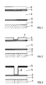
- FIGS. 1 to 14 show the process sequence, including some process variants for producing a gate electrode which is mushroom-shaped in cross section.
- a mushroom-shaped gate electrode with a small footprint and an extensive overhang is produced by means of the method described below.
- the invention uses a 5-layer technique, the structure of which is shown in FIG. 1.
- a semiconductor substrate e.g. GaAs
- an approximately 200 to 500 nm thick first polymer layer e.g. Photoresist AZ4040, applied.
- a thin structuring layer 3 e.g. SiO2, Si3N4 or Ge from about 10 to 50 and then a thick second polymer layer 4, e.g. Photoresist AZ 4110 from about 500 to 1100nm deposited.
- This top layer 6 consists either of a photoresist for optical lithography, e.g. Photoresist AZ4040, or from an electron sensitive photoresist for electron optical exposure, e.g. PMMA, to achieve the finest structures.
- the invention uses etching processes, e.g. Plasma etching.
- the individual etching processes must have the highest possible selectivity between the polymer layers 2, 4, 6 and the structuring layers 3, 5.
- the base structure 7 of the gate contact is produced lithographically in the top polymer layer (FIG. 2).
- the base structure 7 is then introduced into the upper structuring layer 5 via a dry etching step and then this structure is transferred exactly to the lower structuring layer 3 by means of anisotropic RIE (reactive ion etching) etching.
- the upper polymer layer 6 is removed and the trench 8 is formed perpendicular to the layers 4, 5 (FIG. 3).
- a The following isotropic dry etching step produces an underetching of the upper structuring layer 5 and the trench 9 (FIG. 4) expanded downward is formed in the second polymer layer 4.
- a window in the lower structuring layer 3 is opened and a subsequent anisotropic RIE etching process transfers the base structure down to the substrate surface.
- the mushroom-shaped trench 10 is formed (FIG. 5).
- the overhang 11 of the upper structuring layer 5 serves as an etching mask, since in this etching step it is mainly the reactive ions directed vertically onto the surface that cause the etching.
- the window in the lower structuring layer 3 is opened, the upper structuring layer 5 is removed with the same material from the upper and lower structuring layer.
- the upper structuring layer 5 must therefore be chosen thicker than the lower structuring layer.
- the desired structure 12 is produced (FIG. 6).
- the oblique side walls of the second polymer layer 4 of the mushroom-shaped trench 10 are not covered with gate metal (FIG. 7).
- a subsequent lift-off process of the second polymer layer 4 simultaneously removes the unwanted metal layer 14 above the second polymer layer 4.
- the lower structuring layer 3 and the first polymer layer 2 are etched away or detached and the mushroom-shaped gate electrode 13 has a foot 15 with the original base structure 7 and a wide head 16 (Fig. 8).
- the layer thicknesses of the structuring layers are chosen so thin that there is sufficient transparency of the layers for adjustment purposes in the case of electron beam exposure.
Landscapes
- Junction Field-Effect Transistors (AREA)
- Drying Of Semiconductors (AREA)
Applications Claiming Priority (2)
| Application Number | Priority Date | Filing Date | Title |
|---|---|---|---|
| DE3839770A DE3839770A1 (de) | 1988-11-25 | 1988-11-25 | Verfahren zur herstellung von gate-elektroden |
| DE3839770 | 1988-11-25 |
Publications (3)
| Publication Number | Publication Date |
|---|---|
| EP0370428A2 true EP0370428A2 (fr) | 1990-05-30 |
| EP0370428A3 EP0370428A3 (en) | 1990-11-28 |
| EP0370428B1 EP0370428B1 (fr) | 1995-01-04 |
Family
ID=6367851
Family Applications (1)
| Application Number | Title | Priority Date | Filing Date |
|---|---|---|---|
| EP89121433A Expired - Lifetime EP0370428B1 (fr) | 1988-11-25 | 1989-11-20 | Méthode de fabrication d'électrodes de porte |
Country Status (2)
| Country | Link |
|---|---|
| EP (1) | EP0370428B1 (fr) |
| DE (2) | DE3839770A1 (fr) |
Cited By (5)
| Publication number | Priority date | Publication date | Assignee | Title |
|---|---|---|---|---|
| EP0352736A3 (fr) * | 1988-07-28 | 1991-03-27 | Siemens Aktiengesellschaft | Procédé pour la réalisation d'une structure de laque sur un matériau semiconducteur ayant une ouverture se rétrécissant vers le matériau semiconducteur |
| US5288654A (en) * | 1990-12-26 | 1994-02-22 | Mitsubishi Denki Kabushiki Kaisha | Method of making a mushroom-shaped gate electrode of semiconductor device |
| US5445979A (en) * | 1993-12-28 | 1995-08-29 | Fujitsu Limited | Method of making field effect compound semiconductor device with eaves electrode |
| US5583063A (en) * | 1993-11-30 | 1996-12-10 | Nec Corporation | Method of forming T-shaped, cross-sectional pattern using two layered masks |
| WO2003096399A1 (fr) * | 2002-05-11 | 2003-11-20 | United Monolithic Semiconductors Gmbh | Procede de production d'un composant semi-conducteur et composant semi-conducteur ainsi produit |
-
1988
- 1988-11-25 DE DE3839770A patent/DE3839770A1/de not_active Withdrawn
-
1989
- 1989-11-20 DE DE58908855T patent/DE58908855D1/de not_active Expired - Fee Related
- 1989-11-20 EP EP89121433A patent/EP0370428B1/fr not_active Expired - Lifetime
Non-Patent Citations (2)
| Title |
|---|
| IEEE ELECTRON DEVICE LETTERS, Band EDL-7, Nr. 2, Februar 1986, Seiten 69-70, IEEE, New York, US; H.M. MACKSEY: "GaAs power FET's having the gate recess narrower than the gate" * |
| JOURNAL OF THE ELECTROCHEMICAL SOCIETY, Band 133, Nr. 10, Oktober 1986, Seiten 409-416, Manchester, NH, US; C.E. WEITZEL et al.: "A review of GaAs MESFET gate electrode fabrication technologies" * |
Cited By (7)
| Publication number | Priority date | Publication date | Assignee | Title |
|---|---|---|---|---|
| EP0352736A3 (fr) * | 1988-07-28 | 1991-03-27 | Siemens Aktiengesellschaft | Procédé pour la réalisation d'une structure de laque sur un matériau semiconducteur ayant une ouverture se rétrécissant vers le matériau semiconducteur |
| US5288654A (en) * | 1990-12-26 | 1994-02-22 | Mitsubishi Denki Kabushiki Kaisha | Method of making a mushroom-shaped gate electrode of semiconductor device |
| US5583063A (en) * | 1993-11-30 | 1996-12-10 | Nec Corporation | Method of forming T-shaped, cross-sectional pattern using two layered masks |
| US5445979A (en) * | 1993-12-28 | 1995-08-29 | Fujitsu Limited | Method of making field effect compound semiconductor device with eaves electrode |
| WO2003096399A1 (fr) * | 2002-05-11 | 2003-11-20 | United Monolithic Semiconductors Gmbh | Procede de production d'un composant semi-conducteur et composant semi-conducteur ainsi produit |
| US7041541B2 (en) | 2002-05-11 | 2006-05-09 | United Monolithic Semiconductors Gmbh | Method for producing a semiconductor component, and semiconductor component produced by the same |
| US7432563B2 (en) | 2002-05-11 | 2008-10-07 | United Monolithic Semiconductors Gmbh | Method for producing a semiconductor component and semiconductor component produced by the same |
Also Published As
| Publication number | Publication date |
|---|---|
| EP0370428A3 (en) | 1990-11-28 |
| DE3839770A1 (de) | 1990-05-31 |
| DE58908855D1 (de) | 1995-02-16 |
| EP0370428B1 (fr) | 1995-01-04 |
Similar Documents
| Publication | Publication Date | Title |
|---|---|---|
| EP0283546B1 (fr) | Procédé pour la fabrication de composants micromécaniques, de n'importe quelle forme, à partir de plaques plans parallèles en polymère, et des traversées dans celles-ci | |
| DE3706127C2 (fr) | ||
| EP0352736B1 (fr) | Procédé pour la réalisation d'une structure de laque sur un matériau semiconducteur ayant une ouverture se rétrécissant vers le matériau semiconducteur | |
| DE19548056C1 (de) | Verfahren zur Herstellung einer Gateelektrode für eine MOS-Struktur | |
| EP0057254B1 (fr) | Procédé de réalisation des structures entrêmement fines | |
| DE19929239A1 (de) | Verfahren zur Herstellung von Halbleitern | |
| DE19938072A1 (de) | Verfahren zum selbstjustierenden Herstellen von zusätzlichen Strukturen auf Substraten mit vorhandenen ersten Strukturen | |
| DE3939319A1 (de) | Asymmetrischer feldeffekttransistor und verfahren zu seiner herstellung | |
| EP0001038B1 (fr) | Procédé de fabrication d'un masque de silicium et son utilisation | |
| DE4413152A1 (de) | Verfahren zur Strukturerzeugung in einem Halbleiterbauelement | |
| DE4446850C2 (de) | Verfahren zur Herstellung eines Transistors für eine Halbleitervorrichtung | |
| EP0370428B1 (fr) | Méthode de fabrication d'électrodes de porte | |
| DE68922474T2 (de) | Verfahren zum Herstellen einer integrierten Schaltung einschliesslich Schritte zum Herstellen einer Verbindung zwischen zwei Schichten. | |
| EP0257328B1 (fr) | Procédé pour fabriquer des jonctions du type PN | |
| DE69534412T2 (de) | III-V-Halbleiterstruktur und Verfahren zu deren Herstellung | |
| DE19945170B4 (de) | Verfahren zur Herstellung einer Schablonenmaske | |
| EP1344245B1 (fr) | Procede pour realiser un corps solide dote d'une microstructure | |
| DE69508273T2 (de) | Verfahren zum ätzen von siliziumnitrid mit verstärkung der kritischen abmessung | |
| EP0003733B1 (fr) | Procédé pour la génération de fenêtres échelonnées dans des couches de matière isolante ou de matière d'électrode pour la production de circuits intégrés à semiconducteur et transistor MIS à effet de champ avec courte longueur de canal fabriqué par ce procédé | |
| WO2003105211A1 (fr) | Procede de production d'un transistor bipolaire a heterojonction et transistor bipolaire a heterojonction | |
| EP1380047B1 (fr) | Procede de production d'un composant semi-conducteur presentant une electrode de contact en forme de t | |
| DE19846691C1 (de) | Verfahren zur Mikrostrukturierung von Gläsern | |
| EP0358042B1 (fr) | Procédé autoaligné pour la fabrication d'une électrode de porte | |
| DE3901288A1 (de) | Verfahren zur herstellung von gate-elektroden | |
| DE2046872A1 (de) | Verfahren zur Herstellung einer Halb leitervornchtung Soieta Generale Semicondutton SpA SGS, Agrate, Mailand (Italien) |
Legal Events
| Date | Code | Title | Description |
|---|---|---|---|
| PUAI | Public reference made under article 153(3) epc to a published international application that has entered the european phase |
Free format text: ORIGINAL CODE: 0009012 |
|
| AK | Designated contracting states |
Kind code of ref document: A2 Designated state(s): DE FR GB IT |
|
| PUAL | Search report despatched |
Free format text: ORIGINAL CODE: 0009013 |
|
| AK | Designated contracting states |
Kind code of ref document: A3 Designated state(s): DE FR GB IT |
|
| 17P | Request for examination filed |
Effective date: 19910116 |
|
| RAP1 | Party data changed (applicant data changed or rights of an application transferred) |
Owner name: DAIMLER-BENZ AKTIENGESELLSCHAFT |
|
| 17Q | First examination report despatched |
Effective date: 19930723 |
|
| GRAA | (expected) grant |
Free format text: ORIGINAL CODE: 0009210 |
|
| ITF | It: translation for a ep patent filed | ||
| AK | Designated contracting states |
Kind code of ref document: B1 Designated state(s): DE FR GB IT |
|
| REF | Corresponds to: |
Ref document number: 58908855 Country of ref document: DE Date of ref document: 19950216 |
|
| GBT | Gb: translation of ep patent filed (gb section 77(6)(a)/1977) |
Effective date: 19950222 |
|
| ET | Fr: translation filed | ||
| PGFP | Annual fee paid to national office [announced via postgrant information from national office to epo] |
Ref country code: GB Payment date: 19951018 Year of fee payment: 7 |
|
| PLBE | No opposition filed within time limit |
Free format text: ORIGINAL CODE: 0009261 |
|
| STAA | Information on the status of an ep patent application or granted ep patent |
Free format text: STATUS: NO OPPOSITION FILED WITHIN TIME LIMIT |
|
| PGFP | Annual fee paid to national office [announced via postgrant information from national office to epo] |
Ref country code: FR Payment date: 19951107 Year of fee payment: 7 |
|
| PGFP | Annual fee paid to national office [announced via postgrant information from national office to epo] |
Ref country code: DE Payment date: 19951122 Year of fee payment: 7 |
|
| 26N | No opposition filed | ||
| PG25 | Lapsed in a contracting state [announced via postgrant information from national office to epo] |
Ref country code: GB Effective date: 19961120 |
|
| GBPC | Gb: european patent ceased through non-payment of renewal fee |
Effective date: 19961120 |
|
| PG25 | Lapsed in a contracting state [announced via postgrant information from national office to epo] |
Ref country code: FR Effective date: 19970731 |
|
| PG25 | Lapsed in a contracting state [announced via postgrant information from national office to epo] |
Ref country code: DE Effective date: 19970801 |
|
| REG | Reference to a national code |
Ref country code: FR Ref legal event code: ST |
|
| PG25 | Lapsed in a contracting state [announced via postgrant information from national office to epo] |
Ref country code: IT Free format text: LAPSE BECAUSE OF NON-PAYMENT OF DUE FEES Effective date: 20051120 |