EP0370661A2 - Convertisseur analogique-numérique en pipeline à sous-gammes et auto-étalonnage - Google Patents
Convertisseur analogique-numérique en pipeline à sous-gammes et auto-étalonnage Download PDFInfo
- Publication number
- EP0370661A2 EP0370661A2 EP89311613A EP89311613A EP0370661A2 EP 0370661 A2 EP0370661 A2 EP 0370661A2 EP 89311613 A EP89311613 A EP 89311613A EP 89311613 A EP89311613 A EP 89311613A EP 0370661 A2 EP0370661 A2 EP 0370661A2
- Authority
- EP
- European Patent Office
- Prior art keywords
- analog
- converter
- resolution
- digital
- low
- Prior art date
- Legal status (The legal status is an assumption and is not a legal conclusion. Google has not performed a legal analysis and makes no representation as to the accuracy of the status listed.)
- Withdrawn
Links
- 239000000872 buffer Substances 0.000 claims abstract description 15
- 238000005070 sampling Methods 0.000 claims description 7
- 238000006243 chemical reaction Methods 0.000 abstract description 8
- 238000000034 method Methods 0.000 abstract description 8
- 238000013459 approach Methods 0.000 abstract description 7
- 230000007774 longterm Effects 0.000 abstract description 2
- 238000001514 detection method Methods 0.000 description 9
- 238000012546 transfer Methods 0.000 description 9
- 238000010586 diagram Methods 0.000 description 8
- 230000006870 function Effects 0.000 description 6
- 238000012545 processing Methods 0.000 description 6
- 230000003321 amplification Effects 0.000 description 3
- 238000005516 engineering process Methods 0.000 description 3
- 238000003199 nucleic acid amplification method Methods 0.000 description 3
- 239000004065 semiconductor Substances 0.000 description 3
- 230000003068 static effect Effects 0.000 description 3
- 238000012360 testing method Methods 0.000 description 3
- 239000003990 capacitor Substances 0.000 description 2
- 230000008569 process Effects 0.000 description 2
- 206010035148 Plague Diseases 0.000 description 1
- 241000607479 Yersinia pestis Species 0.000 description 1
- 230000000295 complement effect Effects 0.000 description 1
- 230000000694 effects Effects 0.000 description 1
- 238000012986 modification Methods 0.000 description 1
- 230000004048 modification Effects 0.000 description 1
- 230000002093 peripheral effect Effects 0.000 description 1
- 230000004044 response Effects 0.000 description 1
- 230000035945 sensitivity Effects 0.000 description 1
Images




Classifications
-
- H—ELECTRICITY
- H03—ELECTRONIC CIRCUITRY
- H03M—CODING; DECODING; CODE CONVERSION IN GENERAL
- H03M1/00—Analogue/digital conversion; Digital/analogue conversion
- H03M1/10—Calibration or testing
- H03M1/1009—Calibration
- H03M1/1033—Calibration over the full range of the converter, e.g. for correcting differential non-linearity
- H03M1/1038—Calibration over the full range of the converter, e.g. for correcting differential non-linearity by storing corrected or correction values in one or more digital look-up tables
-
- H—ELECTRICITY
- H03—ELECTRONIC CIRCUITRY
- H03M—CODING; DECODING; CODE CONVERSION IN GENERAL
- H03M1/00—Analogue/digital conversion; Digital/analogue conversion
- H03M1/12—Analogue/digital converters
- H03M1/34—Analogue value compared with reference values
- H03M1/38—Analogue value compared with reference values sequentially only, e.g. successive approximation type
- H03M1/44—Sequential comparisons in series-connected stages with change in value of analogue signal
Definitions
- the present invention generally relates to analog-to-digital (A/D) converters and, more particularly, to a new architecture to realize fast, high resolution A/D converters in high-reliability VLSI monolithic semiconductor technology.
- A/D analog-to-digital
- VLSI very large scale integrated
- a fully parallel A/D converter architecture is described in an article entitled "A Fully Parallel 10-Bit A/D Converter with Video Speed: by Toyoki Takemoto, Michihiro Inoue, Hideaki Sadamatsu, Akira Matsuzawa, and Kazuhiko Tsuji in IEEE Journal of Solid-State Circuits, vol. SC-17, no. 6, pp. 1133 to 1138 (Dec. 1982).
- the fully parallel architecture described requires 2 m- 1 comparators to achieve m bits of resolution.
- a two-step flash A/D converter architecture is described in an article entitled "An 8-MHz CMOS Subranging 8-Bit A/D Converter” by Andrew G.F. Dingwall and Victor Zazzu in IEEE Journal of Solid-State Circuits, vol. SC-20, no. 6, pp. 1138 to 1143 (Dec. 1985).
- the two-step flash architecture described requires 2' "' -1 comparators to achieve m bits of resolution.
- CMOS complementary metal-oxide-semiconductor
- a self-calibrating pipelined subranging analog-to-digital converter comprises sample-and-hold means for sampling an analog signal which is to be converted to a digital output code, and a pipeline of elemental stages connected for sampling the analog signal to generate a low-resolution output digital code.
- Calibration means are provided and include memory and arithmetic means addressed by the low-resolution output digital code for storing nonlinearity information and computing a second output digital code based on an interpolation of the low-resolution output digital code with the nonlinearity information.
- a high-resolution analog-to-digital converter is connected to the sample-and-hold means and, in response to samples of the analog signal, generates a high-resolution output digital code which serves as a reference.
- the calibration means is periodically responsive to the high resolution output digital code for calibrating the memory and arithmetic means.
- FIGs 1 and 2 which show the architecture of a pipelined subranging A/D converter in accordance with the invention
- the converter is shown to be made up of a clocked pipeline of elemental stages.
- Each stage 10 i , 10z, ..., 10k of the pipeline is comprised, as shown in Figure 2, of a low-resolution n t -bit flash A/D subconverter 12, two n i -bit digital-to-analog (D/A) converters 14, and a unity-gain buffer 16.
- the analog input signal for each respective stage of the pipelined A/D converter is sampled successively through a plurality of sample-and-hold (S/H) circuits 18 1 , 18 2 , . .
- S/H sample-and-hold
- each S/H circuit delivers its held signal V a1 , V a2 ...V ak , respectively, as voltages V aj , V aj-1 ...V aj-k-1 , respectively, to each of the pipeline stages sequentially through a switching circuit 11 such as a continually-clocked shift register.
- the pipeline stages, sample-and-hold circuits, and switching circuit are all driven in common by a clock (not shown, for simplicity of illustration).
- each sample-and-hold circuit With each clock cycle, the held voltage in each sample-and-hold circuit is supplied to the next-successive pipeline stage, and the sample-and-hold circuit that had been coupled to the final stage 10 k of the pipelined A/D converter takes a new sample of the analog input voltage V analog which is held and supplied to the first stage 10, of the pipelined A/D converter.
- the analog input signal V aj of each stage of the pipelined A/D converter is converted by the A/D subconverter 12 of that stage to n f bits.
- the A/D subconverter receives its reference voltages (V refi and -V refi ) from the immediately preceding stage of the pipelined A/D converter.
- the n bits are sent to the D/A converters 14 which generate the corresponding sub-reference voltages (V ni+1.5 and V ni-0.5 ). These voltages are then delivered as voltages V ni+1.5 and V ni-0.5 to the next following stage as its reference voltages through unity-gain buffer 16.
- subscript i as used in conjunction with a voltage, signifies input voltages to any stage as being received from the immediately preceding stage and output voltages from any stage being applied to the next successive stage, while the subscript j signifies the sampled analog voltage supplied to any given one (j) of the pipelined A/D converter stages by a corresponding one of the sample-and-hold circuits.
- the A/D subconverter 12 in each of the pipeline stages can in principle be implemented by any known A/D converter scheme, such as flash, successive-approximation, oversampled delta-sigma, etc. Similar consideration applies to the D/A converters 14 in each of the pipeline stages.
- Figure 3 is a more detailed example of one stage of a high-speed pipelined A/D converter where a flash A/D subconverter 12 and two resistive D/A converters 14a and 14b are employed.
- the amplified difference signal between the analog input voltage and the reference voltage of each comparator is squared up and latched to produce a logic level.
- a decoder and encoder 24 such as the interconnected decoder and encoder shown and described in S.T. Chu et al. U.S. patent 4,768,016, issued August 20, 1988 and assigned to the present applicants, interprets the comparator outputs and selects the appropriate code from the encoder portion to produce a conversion result with n i bits of resolution.
- the resulting conversion signal is supplied to the switch networks 25a and 25b of the respective D/A converters 14a and 14b to select the corresponding reference voltage range (or "subrange") and deliver it to the next pipeline stage through unity-gain buffer 16.
- switch networks 25a and 25b are represented as being made up of mechanical switches for ease of understanding, the switches are actually implemented electronically in a manner well known to those skilled in the art.
- the voltage window for the following stage is doubled to tolerate and correct errors. For instance, when a given analog input signal falls into the voltage range between taps p and q on the resistors R of resistor string 22a shown in Figure 3, the switch network 25a will select and deliver the voltage window between taps r and t to the following stage. In this way, the following stage will generate an extra bit which can be used to correct the digital error of the previous stage.
- This "double-window" scheme relaxes the stringent requirements that necessitate use of high-precision comparators and the unity-gain buffers are allowed to have offsets large compared to 1/2 LSB.
- the comparators in the last stage require the highest resolution since the subrange in the last stage is the narrowest among all the pipeline stages. To relax this stringent resolution requirement, the last stage is modified such that the residual voltage from the previous stage is amplified and delivered to the last stage as its analog input signal. In this way, a coarse amplifier with n k bits of accuracy and the relaxed comparators with 1/2"2 nk ⁇ LSB of resolution will satisfy the performance requirements.
- the sub-reference voltage from the first stage must be accurate to m-bit level; any deviation from this will affect the integral linearity of the converter.
- the sub-reference voltages from the subsequent stages are only required to be accurate to the bit level, where h is the order of the pipeline stage of interest.
- a reference resistor string with more than 9 to 10 bits of accuracy is very difficult to realize.
- a capacitive D/A converter array based on charge redistribution can be employed in the first pipeline stage in order to achieve the required accuracy.
- the pipelining and concurrency features of the pipelined subranging architecture result in high throughput of the converter.
- the first stage is converting the most recent sample (V aj ) with a full voltage range
- the next stage is converting the previous sample (V aj . 1 ) with a "subrange" generated from the previous stage
- the next stage is converting the sample previous to that (V aj . 2 ), and so forth.
- This pipelining scheme achieves a throughput rate at one sample per clock cycle, the same as that in the pure flash converter.
- each stage of the pipeline can have relatively low resolution, making the associated hardware complexity relatively low compared to a pure flash or two-step flash converter.
- the pipelined subranging architecture does not require analog processing (i.e., subtraction and amplification) as in the conventional pipelined approach. Any concern about encountering unknown offset and gain errors that plague the conventional pipelined architecture due to analog processing can thus be relieved.
- the linearity errors (d, e 2 and e 3 ) at each turning point of the curve can be detected and stored in the RAM.
- the gain should be adjusted for the first section of the curve, and both the gain and offset should be adjusted for the remaining sections.
- the transfer characteristic of the converter can be improved to that shown in Figure 4B, where the linearity errors at the one-quarter, one-half and three-quarter points of the transfer curve are eliminated.
- the non-ideal transfer characteristic can be calibrated more accurately with more section approximation.
- n is the number of bits of resolution of the first pipeline stage.
- the linearity error (e x ) at any given output code can be computed by using the interpolation method as shown in Figure 4C.
- equation (1) can be expressed in the following digital form, This computation can be performed in the digital circuitry using shift registers and binary tree adders.
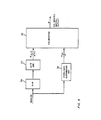
- FIG. 5 A block diagram of the monolithic A/D converter system that implements the above calibration algorithm is shown in Figure 5.
- the system comprises a pipelined subranging A/D converter 30 (of the type shown in Figure 1) to be calibrated, a high-precision but low speed A/D converter 32 such as an over-sampled delta-sigma converter, and a calibrator 34.
- An analog signal entering the system is delivered in parallel to the two converters.
- a sample-and-hold (S/H) circuit 36 samples the analog signal for the delta-sigma converter 32.
- the delta-sigma converter 32 has two more bits of resolution than the pipelined subranging converter 30 and provides an ideal transfer characteristic for calibration. There are two operating modes in the system; an error detection mode and the normal conversion mode.
- the pipelined subranging A/D converter 30 output signal comprised of certain samples is compared with the delta-sigma converter 32 output signal and the difference is detected and stored in a random access memory (RAM) portion of calibrator 34.
- the pipelined subranging A/D converter 30 output signal accesses the stored information to compute its corresponding linearity error (e x ) and to cancel its nonlinearity.
- FIG. 6 is a block diagram of the calibrator 34 of Figure 5
- Figure 7 is a flow diagram illustrating the basic sequence of error detection in the calibrator.
- the calibrator comprises an m-bit comparator 40, an (m + 2)-bit subtractor 42 having one input coupled to the output of comparator 40 through a buffer 54 and a second input receiving the digital output signal (D ⁇ - ⁇ ) from slow delta-sigma A/D converter 32 (shown in Figure 5).
- the output of an n 1 -bit counter 46 which counts a number designated x, is coupled to one input of comparator 40 and to the W ADDR (or Write Address) port of a dual-port static random access memory (RAM) 50.
- W ADDR or Write Address
- the output of an s-bit counter 48 which counts a number designated y, is coupled to one input of an accumulator 44 having a second input coupled to the output of subtractor 42.
- the accumulator comprises a shift register 45 and an adder 47, the output of each being coupled to the input of the other, respectively.
- the digital output signal (Dp s ) from the pipelined subranging A/D converter 30 (shown in Figure 5) is supplied to a second input of comparator 40, the second port designated R ADDR (or Read Address) of dual-port static RAM 50, and to a first input of an arithmetic unit 52 that computes e x according to equation (2).
- the arithmetic unit receives, as a second input, the output signal of dual-port static RAM 50.
- the error detection mode begins by comparing the digital output signal Dp s from the pipelined subranging A/D converter 30 with the output signal of counter 46.
- Dp s is delivered to the buffer 54, as indicated by the test in decision block 60 of Figure 7. Otherwise, a reset signal is generated to reset the sample-and-hold circuit 36 (shown in Figure 5) as well as delta-sigma converter 32 ( Figure 5) to take and convert the next sample, as indicated by function block 62.
- Digital signal Dp s stays in the buffer 54 until the slow delta-sigma converter 32 produces a high precision digital value D ⁇ - ⁇ corresponding to the sample being held.
- the linearity error (e;) with respect to signal D ps is determined by subtracting D ⁇ - ⁇ from Dp s in subtractor 42, as indicated in function block 64.
- offset error e i corresponding to a given digital signal Dp s is detected several times before being stored in RAM 50. This is accomplished by temporarily storing the offset error e; in accumulator 44, as indicated in function block 66, and repeating the error detection sequence 2 5 times, as determined by the test presented in decision block 68.
- Counter 48 counts the number of occurrences of offset error e i detection. Once the output count of counter 48 reaches 2 5 , the accumulated result is divided by 2 5 in shift register 45 of the accumulator to produce an averaged offset error e i , as indicated by function block 70. This averaged offset error e i is then stored in RAM 50 at the address equal to the output count of counter 46.
- the RAM 50 may be a 100-bit memory.
- Counter 48 counts much faster than counter 46.
- Counter 48 counts to 2 s , where s is an arbitrary number defined by the user to average the error. Typically, s might be set equal to 5.
- Counter 46 counts to 2 n1 , where ni is the resolution of the first pipeline stage. In an implemented prototype of the system, ni wad set to equal 4.
- the error detection process continues by incrementing counter 46, as indicated in function block 72, and detecting the linearity error with respect to the next bit pattern constructed by n i most significant bits (MSBs) of digital signal D ps , as determined according to the test presented in decision block 74.
- MSBs most significant bits
- n i bits of pipelined subranging A/D converter 30 output signal access its corresponding nonlinearity terms (e j , e i+1 ) from RAM 50. These terms are delivered to the arithmetic unit to compute its corresponding linear error (e x ) according to equation (2). This linearity error (e x ) is then subtracted from the pipelined subranging A/D converter output signal Dp s to cancel its nonlinearity.
- the error detection mode can be performed concurrently with normal conversion mode to frequently update the error terms (e;) stored in RAM 50. Any long term drift of components due to temperature or environment variations can be detected and corrected.
Landscapes
- Physics & Mathematics (AREA)
- Nonlinear Science (AREA)
- Engineering & Computer Science (AREA)
- Theoretical Computer Science (AREA)
- Analogue/Digital Conversion (AREA)
- Compression, Expansion, Code Conversion, And Decoders (AREA)
Applications Claiming Priority (2)
| Application Number | Priority Date | Filing Date | Title |
|---|---|---|---|
| US275819 | 1988-11-25 | ||
| US07/275,819 US4894656A (en) | 1988-11-25 | 1988-11-25 | Self-calibrating pipelined subranging analog-to-digital converter |
Publications (2)
| Publication Number | Publication Date |
|---|---|
| EP0370661A2 true EP0370661A2 (fr) | 1990-05-30 |
| EP0370661A3 EP0370661A3 (fr) | 1992-04-15 |
Family
ID=23053930
Family Applications (1)
| Application Number | Title | Priority Date | Filing Date |
|---|---|---|---|
| EP19890311613 Withdrawn EP0370661A3 (fr) | 1988-11-25 | 1989-11-09 | Convertisseur analogique-numérique en pipeline à sous-gammes et auto-étalonnage |
Country Status (3)
| Country | Link |
|---|---|
| US (1) | US4894656A (fr) |
| EP (1) | EP0370661A3 (fr) |
| JP (1) | JPH02223227A (fr) |
Cited By (7)
| Publication number | Priority date | Publication date | Assignee | Title |
|---|---|---|---|---|
| WO1998011668A1 (fr) * | 1996-09-16 | 1998-03-19 | Audiologic Hearing Systems, L.P. | Numeriseur a plage dynamique large |
| EP0709971A3 (fr) * | 1994-10-28 | 1998-05-06 | Harris Corporation | Convertisseur analogique-numérique sigma delta à trois points et méthode associée |
| EP0849883A1 (fr) * | 1992-10-01 | 1998-06-24 | Matsushita Electric Industrial Co., Ltd. | Convertisseur analogique numérique |
| WO2001069791A1 (fr) * | 2000-03-14 | 2001-09-20 | Telefonaktiebolaget Lm Ericsson | Calibrage de fond d'un convertisseur analogique/numerique |
| EP0945987A3 (fr) * | 1998-03-26 | 2003-02-12 | Italtel s.p.a. | Procédé de linéarisation de la caractéristique de transfert d'un convertisseur N/A et circuit pour celui-ci |
| FR2858140A1 (fr) * | 2003-07-22 | 2005-01-28 | Denso Corp | Procede et dispositif de correction de non-linearite pour donnees de sortie de conversion a/n |
| CN101924556A (zh) * | 2009-06-12 | 2010-12-22 | 台湾积体电路制造股份有限公司 | 集成电路、系统与模拟信号转换至数字信号的方法 |
Families Citing this family (39)
| Publication number | Priority date | Publication date | Assignee | Title |
|---|---|---|---|---|
| EP0360919B1 (fr) * | 1988-09-30 | 1995-12-20 | Siemens Aktiengesellschaft | Procédé de détermination et de traitement de valeurs de correction pour des convertisseurs A/N et N/A à auto-étalonnage et unité de calcul pour la mise en fonction du procédé |
| US5047772A (en) * | 1990-06-04 | 1991-09-10 | General Electric Company | Digital error correction system for subranging analog-to-digital converters |
| US5196851A (en) * | 1991-05-24 | 1993-03-23 | Samsung Electronics Co., Ltd. | Linearizing non-linear analog-to-digital process and circuit |
| US5182558A (en) * | 1991-10-25 | 1993-01-26 | Halliburton Geophysical Services, Inc. | System for generating correction signals for use in forming low distortion analog signals |
| US5221926A (en) * | 1992-07-01 | 1993-06-22 | Motorola, Inc. | Circuit and method for cancelling nonlinearity error associated with component value mismatches in a data converter |
| US5416485A (en) * | 1993-12-20 | 1995-05-16 | Lee; Hae-Seung | Analog-to-digital conversion circuit with improved differential linearity |
| KR970005828B1 (ko) * | 1993-12-31 | 1997-04-21 | 김정덕 | 파이프 라인 구조의 다단 아날로그/디지탈 변환기 |
| US5499027A (en) * | 1994-02-24 | 1996-03-12 | Massachusetts Institute Of Technology | Digitally self-calibrating pipeline analog-to-digital converter |
| US5552784A (en) * | 1994-06-30 | 1996-09-03 | Northrop Grumman Corporation | Distortion reduction circuit for analog to digital converter system |
| WO1996009692A1 (fr) * | 1994-09-23 | 1996-03-28 | National Semiconductor Corporation | Architecture efficace de correction des defauts de non-concordance des composants et des non-linearites des circuits d'un convertisseur a/n |
| JP3581485B2 (ja) * | 1996-04-05 | 2004-10-27 | 株式会社ルネサステクノロジ | パイプライン型a/dコンバータ |
| JP3597303B2 (ja) * | 1996-04-23 | 2004-12-08 | 株式会社ルネサステクノロジ | A/dコンバータのテスト方法及びテスト装置 |
| JP3597636B2 (ja) * | 1996-05-07 | 2004-12-08 | 株式会社ルネサステクノロジ | サブレンジング型a/d変換器 |
| US5731775A (en) * | 1996-06-17 | 1998-03-24 | Lucent Technologies Inc. | Subranging converter with plurality of resistor strings and transistor switches |
| US5717396A (en) * | 1996-06-17 | 1998-02-10 | Lucent Technologies Inc. | Analog-to-digital converter signal storage capacitor perturbation |
| DE19631972C2 (de) * | 1996-08-08 | 1998-07-02 | Bosch Gmbh Robert | Verfahren zum Überwachen der Funktionsfähigkeit eines zur Digitalisierung von Analogsignalen ausgelegten Analog/-Digital Wandlers |
| US5771012A (en) * | 1996-09-11 | 1998-06-23 | Harris Corporation | Integrated circuit analog-to-digital converter and associated calibration method and apparatus |
| KR100286322B1 (ko) * | 1997-09-11 | 2001-04-16 | 김영환 | 아날로그/디지털변환회로 |
| US6198423B1 (en) * | 1997-12-23 | 2001-03-06 | Texas Instruments Incorporated | Analog-to-digital converter system having enhanced digital self-calibration |
| US6198417B1 (en) | 1998-01-29 | 2001-03-06 | Massachusetts Institute Of Technology | Pipelined oversampling A/D converter |
| US6169502B1 (en) * | 1998-05-08 | 2001-01-02 | Cirrus Logic, Inc. | Pipelined analog-to-digital converter (ADC) systems, methods, and computer program products |
| US6121912A (en) * | 1998-09-30 | 2000-09-19 | National Semiconductor Corporation | Subranging analog-to-digital converter and method |
| US6348888B1 (en) * | 1999-03-22 | 2002-02-19 | Texas Instruments Incorporated | Pipelined ADC with noise-shaped interstage gain error |
| US6466162B2 (en) | 2000-02-16 | 2002-10-15 | Bertho Boman | System and method for measuring distance between two objects |
| US6304211B1 (en) | 2000-02-16 | 2001-10-16 | Bertho Boman | System and method for measuring distance between two objects using received satellite transmitted data |
| US6445315B1 (en) * | 2001-07-12 | 2002-09-03 | Cirrus Logic, Inc. | Calibration of isolated analog-to-digital converters |
| US6570523B1 (en) * | 2002-02-13 | 2003-05-27 | Intersil Americas Inc. | Analog to digital converter using subranging and interpolation |
| US6714886B2 (en) * | 2002-02-13 | 2004-03-30 | Eric C. Sung | System and method of DC calibration of amplifiers |
| US7577212B2 (en) * | 2004-08-30 | 2009-08-18 | Micron Technology, Inc. | Method and system for generating reference voltages for signal receivers |
| JP4829695B2 (ja) | 2006-06-16 | 2011-12-07 | パナソニック株式会社 | A/d変換器 |
| US7796067B2 (en) * | 2008-04-08 | 2010-09-14 | Standard Microsystems Corporation | Curvature correction methodology |
| FR2966663B1 (fr) * | 2010-10-26 | 2013-07-05 | St Microelectronics Grenoble 2 | Dispositif et procede de traitement d'un signal analogique |
| US8441378B2 (en) * | 2011-08-11 | 2013-05-14 | Pixart Imaging, Inc. | Capacitor mismatch error correction in pipeline analog-to-digital converters |
| JP5792644B2 (ja) * | 2012-01-13 | 2015-10-14 | 株式会社東芝 | 残差信号発生回路、逐次比較型ad変換器、パイプライン型ad変換器および無線受信機 |
| JP5758434B2 (ja) * | 2013-05-08 | 2015-08-05 | 株式会社半導体理工学研究センター | Δσa/d変換装置 |
| KR102267398B1 (ko) * | 2015-01-27 | 2021-06-21 | 삼성전자주식회사 | 신호 처리 장치 및 방법 |
| US10469096B1 (en) * | 2019-01-03 | 2019-11-05 | Esilicon Corporation | Successive approximation register (SAR) analog to digital converter (ADC) with partial loop-unrolling |
| US10454491B1 (en) * | 2019-01-03 | 2019-10-22 | Esilicon Corporation | Successive approximation register (SAR) analog to digital converter (ADC) with partial loop-unrolling |
| DE102020114244B4 (de) * | 2020-05-27 | 2024-11-28 | WAGO Verwaltungsgesellschaft mit beschränkter Haftung | Vorrichtungen und verfahren zur messwertkalibrierung |
Family Cites Families (8)
| Publication number | Priority date | Publication date | Assignee | Title |
|---|---|---|---|---|
| US3725903A (en) * | 1971-02-09 | 1973-04-03 | Bendix Corp | Self-calibrating analog to digital converter |
| US3961325A (en) * | 1974-07-15 | 1976-06-01 | Fairchild Camera And Instrument Corporation | Multiple channel analog-to-digital converter with automatic calibration |
| NL7712273A (nl) * | 1977-11-08 | 1979-05-10 | Philips Nv | Werkwijze en inrichting voor het automatisch ijken van een analoog-digitaal-omzetter. |
| US4222107A (en) * | 1979-01-22 | 1980-09-09 | Burr-Brown Research Corporation | Method and apparatus for automatically calibrating a digital to analog converter |
| DE2912925C2 (de) * | 1979-03-31 | 1986-06-26 | Licentia Patent-Verwaltungs-Gmbh, 6000 Frankfurt | Verfahren und Anordnung zur schnellen hochauflösenden Analog/Digital-Umsetzung mit selbständiger Korrektur |
| US4342983A (en) * | 1980-08-11 | 1982-08-03 | Westinghouse Electric Corp. | Dynamically calibrated successive ranging A/D conversion system and D/A converter for use therein |
| US4612533A (en) * | 1985-06-12 | 1986-09-16 | The United States Of America As Represented By The Secretary Of The Air Force | Harmonic distortion reduction technique for data acquistion |
| US4700174A (en) * | 1986-05-12 | 1987-10-13 | Westinghouse Electric Corp. | Analog signal processor |
-
1988
- 1988-11-25 US US07/275,819 patent/US4894656A/en not_active Expired - Lifetime
-
1989
- 1989-11-09 EP EP19890311613 patent/EP0370661A3/fr not_active Withdrawn
- 1989-11-14 JP JP1294121A patent/JPH02223227A/ja active Pending
Cited By (9)
| Publication number | Priority date | Publication date | Assignee | Title |
|---|---|---|---|---|
| EP0849883A1 (fr) * | 1992-10-01 | 1998-06-24 | Matsushita Electric Industrial Co., Ltd. | Convertisseur analogique numérique |
| EP0709971A3 (fr) * | 1994-10-28 | 1998-05-06 | Harris Corporation | Convertisseur analogique-numérique sigma delta à trois points et méthode associée |
| WO1998011668A1 (fr) * | 1996-09-16 | 1998-03-19 | Audiologic Hearing Systems, L.P. | Numeriseur a plage dynamique large |
| EP0945987A3 (fr) * | 1998-03-26 | 2003-02-12 | Italtel s.p.a. | Procédé de linéarisation de la caractéristique de transfert d'un convertisseur N/A et circuit pour celui-ci |
| WO2001069791A1 (fr) * | 2000-03-14 | 2001-09-20 | Telefonaktiebolaget Lm Ericsson | Calibrage de fond d'un convertisseur analogique/numerique |
| JP2003527027A (ja) * | 2000-03-14 | 2003-09-09 | テレフオンアクチーボラゲツト エル エム エリクソン | A/d変換器バックグラウンド・キャリブレーション |
| FR2858140A1 (fr) * | 2003-07-22 | 2005-01-28 | Denso Corp | Procede et dispositif de correction de non-linearite pour donnees de sortie de conversion a/n |
| CN101924556A (zh) * | 2009-06-12 | 2010-12-22 | 台湾积体电路制造股份有限公司 | 集成电路、系统与模拟信号转换至数字信号的方法 |
| CN101924556B (zh) * | 2009-06-12 | 2015-07-01 | 台湾积体电路制造股份有限公司 | 集成电路、系统与模拟信号转换至数字信号的方法 |
Also Published As
| Publication number | Publication date |
|---|---|
| US4894656A (en) | 1990-01-16 |
| JPH02223227A (ja) | 1990-09-05 |
| EP0370661A3 (fr) | 1992-04-15 |
Similar Documents
| Publication | Publication Date | Title |
|---|---|---|
| US4894656A (en) | Self-calibrating pipelined subranging analog-to-digital converter | |
| US6124818A (en) | Pipelined successive approximation analog-to-digital converters | |
| US6489904B1 (en) | Pipeline analog-to-digital converter with on-chip digital calibration | |
| US5635937A (en) | Pipelined multi-stage analog-to-digital converter | |
| KR101020672B1 (ko) | 비동기 전류모드 순환 비교를 이용한 아날로그-디지털 변환 | |
| KR100332243B1 (ko) | 파이프라인형아날로그-디지탈변환기용기수2아키텍쳐및교정기법 | |
| US5929796A (en) | Self-calibrating reversible pipeline analog to digital and digital to analog converter | |
| US4894657A (en) | Pipelined analog-to-digital architecture with parallel-autozero analog signal processing | |
| US6222471B1 (en) | Digital self-calibration scheme for a pipelined A/D converter | |
| US9059730B2 (en) | Pipelined successive approximation analog-to-digital converter | |
| US8294607B2 (en) | Multichannel digitizer and method of digitizing | |
| US7075465B2 (en) | Comparator offset calibration for A/D converters | |
| US5572212A (en) | Pipelined analog to digital converter | |
| US4763106A (en) | Flash analog-to-digital converter | |
| US20100182176A1 (en) | Converter circuit, analog/digital converter, and method for generating digital signals corresponding to analog signals | |
| SE500357C2 (sv) | Arrangemang för analog/digital-omvandling | |
| JPH05218868A (ja) | 多段型ad変換器 | |
| EP0698315A1 (fr) | Convertisseur a/n algorithmique a signal de sortie a etalonnage numerique | |
| CN118659783B (zh) | 一种应用于流水线逐次逼近型adc的校准方法及电路 | |
| US5739781A (en) | Sub-ranging analog-to-digital converter with open-loop differential amplifiers | |
| US5173698A (en) | Flash analog-to-digital converter with integrating input stage | |
| Martens et al. | Calibration techniques for optimizing performance of high-speed ADCs | |
| US20060092069A1 (en) | Domino asynchronous successive approximation adc | |
| US6750799B1 (en) | A/D conversion technique using digital averages | |
| EP0930715A2 (fr) | Système d'autocalibration numérique d'un convertisseur a/n à chevauchement |
Legal Events
| Date | Code | Title | Description |
|---|---|---|---|
| PUAI | Public reference made under article 153(3) epc to a published international application that has entered the european phase |
Free format text: ORIGINAL CODE: 0009012 |
|
| AK | Designated contracting states |
Kind code of ref document: A2 Designated state(s): DE FR GB IT NL SE |
|
| PUAL | Search report despatched |
Free format text: ORIGINAL CODE: 0009013 |
|
| AK | Designated contracting states |
Kind code of ref document: A3 Designated state(s): DE FR GB IT NL SE |
|
| 17P | Request for examination filed |
Effective date: 19920930 |
|
| STAA | Information on the status of an ep patent application or granted ep patent |
Free format text: STATUS: THE APPLICATION HAS BEEN WITHDRAWN |
|
| 18W | Application withdrawn |
Withdrawal date: 19930603 |