EP0370831B1 - Halbleiterlaser mit geteilter Elektrode - Google Patents
Halbleiterlaser mit geteilter Elektrode Download PDFInfo
- Publication number
- EP0370831B1 EP0370831B1 EP89312237A EP89312237A EP0370831B1 EP 0370831 B1 EP0370831 B1 EP 0370831B1 EP 89312237 A EP89312237 A EP 89312237A EP 89312237 A EP89312237 A EP 89312237A EP 0370831 B1 EP0370831 B1 EP 0370831B1
- Authority
- EP
- European Patent Office
- Prior art keywords
- layers
- layer
- electrodes
- semiconductor laser
- type
- Prior art date
- Legal status (The legal status is an assumption and is not a legal conclusion. Google has not performed a legal analysis and makes no representation as to the accuracy of the status listed.)
- Expired - Lifetime
Links
Images
Classifications
-
- H—ELECTRICITY
- H01—ELECTRIC ELEMENTS
- H01S—DEVICES USING THE PROCESS OF LIGHT AMPLIFICATION BY STIMULATED EMISSION OF RADIATION [LASER] TO AMPLIFY OR GENERATE LIGHT; DEVICES USING STIMULATED EMISSION OF ELECTROMAGNETIC RADIATION IN WAVE RANGES OTHER THAN OPTICAL
- H01S5/00—Semiconductor lasers
- H01S5/04—Processes or apparatus for excitation, e.g. pumping, e.g. by electron beams
- H01S5/042—Electrical excitation ; Circuits therefor
- H01S5/0425—Electrodes, e.g. characterised by the structure
- H01S5/04254—Electrodes, e.g. characterised by the structure characterised by the shape
-
- H—ELECTRICITY
- H01—ELECTRIC ELEMENTS
- H01S—DEVICES USING THE PROCESS OF LIGHT AMPLIFICATION BY STIMULATED EMISSION OF RADIATION [LASER] TO AMPLIFY OR GENERATE LIGHT; DEVICES USING STIMULATED EMISSION OF ELECTROMAGNETIC RADIATION IN WAVE RANGES OTHER THAN OPTICAL
- H01S5/00—Semiconductor lasers
- H01S5/20—Structure or shape of the semiconductor body to guide the optical wave ; Confining structures perpendicular to the optical axis, e.g. index or gain guiding, stripe geometry, broad area lasers, gain tailoring, transverse or lateral reflectors, special cladding structures, MQW barrier reflection layers
- H01S5/22—Structure or shape of the semiconductor body to guide the optical wave ; Confining structures perpendicular to the optical axis, e.g. index or gain guiding, stripe geometry, broad area lasers, gain tailoring, transverse or lateral reflectors, special cladding structures, MQW barrier reflection layers having a ridge or stripe structure
- H01S5/227—Buried mesa structure ; Striped active layer
Definitions
- This invention relates generally to semiconductor laser devices for producing laser light and, more particularly, to a divided electrode type semiconductor laser device designed to facilitate and improve the separation of the electrodes.
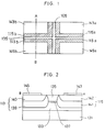
- Fig. 2 shows the structure of a lateral junction type embedded semiconductor laser device of the kind shown in EP 0 342 018, which is a document falling within the term defined by Art 54(3) EPC.
- This laser device includes a double-hetero-structure which is formed on a semi-insulating substrate 131 and in which a GaAs active layer 137 is interposed between undoped AlGaAs clad layers 133 and 135.
- a p-AlGaAs clad layer 139, a p-GaAs cap layer 140, an n-AlGaAs clad layer 141 and an n-GaAs cap layer 142 are formed and embedded on the left-hand and right-hand sides of the GaAs active layer 137 respectively as viewed in Fig. 2, to form carrier injection layers 113 and 115 and electrodes 143 and 145 are formed on these layers.
- a current flowing through the electrodes 143 and 145 is confined between the undoped AlGaAs clad layers 133 and 135 having a high resistance, and carriers are thereby injected into the GaAs active layer 137 having a smaller energy band gap, so that light is generated by recombination of electrons and holes.
- the generated light is confined between and guided by the upper and lower, left and right clad layers, thereby emitting laser light in the direction perpendicular to the plane of projection of Fig. 2.
- This laser device is specifically suitable for integration because of the construction in which the device is constructed on the semi-insulating substrate 131, the carrier injection clad layers are positioned on the opposite sides, and the electrodes are independent of the substrate.
- Fig. 3 is a top view of the semiconductor laser device shown in Fig. 2. As shown in Fig. 3, leads 147 and 149 are connected to the electrodes 143 and 145, a current is supplied through these leads to inject carriers from the buried carrier injection layers 115 and 113 into the active layer, thereby emitting laser light from opposite ends of the device.
- This lateral-junction embedded semiconductor laser device may be divided into a plurality of elements which are independently used for oscillation, control and so on to effect pulse oscillation or the like by controlling laser oscillation.
- the electrodes are divided in such a manner that, as shown in Fig. 4, the carrier injection clad layer and the electrodes are partially removed by gas-phase or liquid-phase etching using HCl gas or H2O2 to form grooves 151 which separate the electrode 143 into electrodes 143a and 143b and the electrode 145 into electrodes 145a and 145b.
- the active layer into which electrons and holes are injected from the left and right clad layers has a small thickness of about 0.2 ⁇ m and a large width of about 2 ⁇ m, and the forward-direction resistance tends to increase. It is therefore necessary to increase the amount of doping for the n-type and p-type clad layers and to form n-type and p-type GaAs cap layers for reducing the resistance of contact with the electrodes. To satisfy these requirements, the facility with which the electrodes are separated as shown in Fig. 4 is sacrificed.
- US-A-4 700 353 discloses lateral junction type quantum well lasers arranged in tandem on a conducting substrate, wherein modulation is achieved by applying voltage between a gate electrode and the substrate.
- an object of the present invention is to provide a semiconductor laser device designed for suitable electrical separation of the electrodes without reducing the amount of doping for the n-type and p-type clad and cap layers and without increasing the forward-direction resistance of the p-n junction.
- a lateral junction type embedded semiconductor laser device as defined in claim 1.
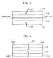
- the semiconductor laser device shown in Figs.land 2 has a semi-insulating substrate 131, undoped AlGaAs clad layers 133 and 135, a GaAs active layer 137, a p-AlGaAs clad layer 139, p-GaAs cap layer 140, an n-AlGaAs clad layer 141, an n-GaAs cap layer 142, an n-electrode 143 and a p-electrode 145.
- a double-hetero-structure in which the GaAs active layer 137 is interposed between the undoped AlGaAs clad layers 133 and 135 is formed on the semi-insulating substrate 131, left and right portions of this structure is removed, and the p-AlGaAs clad layer 139, the p-GaAs cap layer 140, the n-AlGaAs clad layer 141 and the n-GaAs cap layer 142 are selectively grown as carrier injection clad layers 113 and 115 in place of the removed portions.
- This selective growth of the carrier clad injection layers is effected in such a manner that the carrier injection clad layers are embedded like islands as shown in Fig. 1 so that the high-resistance undoped clad layer 135,105 remains between the clad layers 139 and 141.
- the electrodes are formed on each of the carrier injection clad layers thus electrically separated. That is, the embedded p-type carrier injection layer 113 is separated into layers 113a and 113b while the buried n-type carrier injection layer is separated into layers 115a and 115b, and p-electrodes 145a and 145b and n-electrodes 143a and 143b are respectively formed on these separated layers.
- the electrodes are suitably separated electrically since the high-resistance undoped clad layer 135,105 remains between the electrodes 145a, 145b, 143a and 143b.
- the n- and p-clad layers are separated into two elements but, needless to say, it is possible to freely select the number of elements into which these layers are separated.
- each of the electrodes respectively connected to the p-type and n-type layers can be easily divided without reducing the amount of doping for the embedded n-type and p-type carrier injection layers and, hence, without increasing the forward-resistance of the p-n junction.
Landscapes
- Physics & Mathematics (AREA)
- Condensed Matter Physics & Semiconductors (AREA)
- General Physics & Mathematics (AREA)
- Electromagnetism (AREA)
- Optics & Photonics (AREA)
- Geometry (AREA)
- Semiconductor Lasers (AREA)
Claims (1)
- Eine Halbleiterlasereinrichtung umfassend eine doppelte Hetero-Struktur, die auf einem halbisolierenden Substrat (131) gebildet ist, und in der eine einzige aktive Schicht (137) zwischen einer unteren, undotierten Schicht (133) und einer oberen, undotierten AlGaAs Überzugsschicht (135,105) zwischengefügt ist, und Überzugsschichten zur Trägerinjektion (113,115) wie Inseln eingebettet sind, um eine Vielzahl von eingebetteten Laserstrukturen mit lateraler Grenzschicht zu bilden, die in Tandemform angeordnet sind, wobei die genannten Überzugsschichten zur Trägerinjektion (113,105) von jeder der genannten Laserstrukturen eine AlGaAs Überzugsschicht vom p-Typ und n-Typ (139,141) einschließt, wobei auf jeder eine GaAs Abdeckschicht (140,142) gebildet ist, und die Anordnung derart ist, daß die genannten Überzugsschichten zur Ladungsinjektion von jeder Laserstruktur durch einen ersten Bereich (135) der genannten undotierten AlGaAs Überzugsschicht getrennt ist, und daß die genannten Überzugsschichten zur Trägerinjektion von benachbarten Tandemlaserstrukturen durch weitere Bereiche (105) der genannten undotierten AlGaAs Überzugsschicht getrennt sind, und daß Elektroden, die mit den genannten Abdeckschichten verbunden sind, die einzigen Elektroden der Einrichtung bilden.
Applications Claiming Priority (2)
| Application Number | Priority Date | Filing Date | Title |
|---|---|---|---|
| JP63299355A JP2772000B2 (ja) | 1988-11-25 | 1988-11-25 | 電極分離型半導体レーザ装置 |
| JP299355/88 | 1988-11-25 |
Publications (3)
| Publication Number | Publication Date |
|---|---|
| EP0370831A2 EP0370831A2 (de) | 1990-05-30 |
| EP0370831A3 EP0370831A3 (de) | 1991-05-02 |
| EP0370831B1 true EP0370831B1 (de) | 1996-02-28 |
Family
ID=17871484
Family Applications (1)
| Application Number | Title | Priority Date | Filing Date |
|---|---|---|---|
| EP89312237A Expired - Lifetime EP0370831B1 (de) | 1988-11-25 | 1989-11-24 | Halbleiterlaser mit geteilter Elektrode |
Country Status (4)
| Country | Link |
|---|---|
| US (1) | US5018159A (de) |
| EP (1) | EP0370831B1 (de) |
| JP (1) | JP2772000B2 (de) |
| DE (1) | DE68925784T2 (de) |
Families Citing this family (6)
| Publication number | Priority date | Publication date | Assignee | Title |
|---|---|---|---|---|
| US5212702A (en) * | 1992-03-25 | 1993-05-18 | At&T Bell Laboratories | Semiconductor surface emitting laser having reduced threshold voltage and enhanced optical output |
| US5212701A (en) * | 1992-03-25 | 1993-05-18 | At&T Bell Laboratories | Semiconductor surface emitting laser having enhanced optical confinement |
| US5608234A (en) * | 1994-11-14 | 1997-03-04 | The Whitaker Corporation | Semi-insulating edge emitting light emitting diode |
| US5629232A (en) * | 1994-11-14 | 1997-05-13 | The Whitaker Corporation | Method of fabricating semiconductor light emitting devices |
| JP2677232B2 (ja) * | 1995-02-23 | 1997-11-17 | 日本電気株式会社 | 長波長半導体レーザおよびその製造方法 |
| JP3314192B2 (ja) | 2000-04-20 | 2002-08-12 | 独立行政法人産業技術総合研究所 | 光変調回路および光復調回路 |
Family Cites Families (3)
| Publication number | Priority date | Publication date | Assignee | Title |
|---|---|---|---|---|
| JPS60235491A (ja) * | 1984-05-08 | 1985-11-22 | Mitsubishi Electric Corp | 半導体レ−ザ |
| US4700353A (en) * | 1985-08-12 | 1987-10-13 | Cornell Research Foundation, Inc. | Active modulation of quantum well lasers by energy shifts in gain spectra with applied electric field |
| JPH0831658B2 (ja) * | 1988-05-11 | 1996-03-27 | 三菱化学株式会社 | 半導体レーザ及びその製造方法 |
-
1988
- 1988-11-25 JP JP63299355A patent/JP2772000B2/ja not_active Expired - Lifetime
-
1989
- 1989-11-22 US US07/440,522 patent/US5018159A/en not_active Expired - Lifetime
- 1989-11-24 DE DE68925784T patent/DE68925784T2/de not_active Expired - Fee Related
- 1989-11-24 EP EP89312237A patent/EP0370831B1/de not_active Expired - Lifetime
Also Published As
| Publication number | Publication date |
|---|---|
| DE68925784D1 (de) | 1996-04-04 |
| EP0370831A3 (de) | 1991-05-02 |
| US5018159A (en) | 1991-05-21 |
| DE68925784T2 (de) | 1996-09-05 |
| JP2772000B2 (ja) | 1998-07-02 |
| EP0370831A2 (de) | 1990-05-30 |
| JPH02144981A (ja) | 1990-06-04 |
Similar Documents
| Publication | Publication Date | Title |
|---|---|---|
| US5373520A (en) | Surface emitting laser and method of manufacturing the same | |
| KR100252000B1 (ko) | 반도체 발광 소자 | |
| US6259715B1 (en) | Surface emitting semiconductor laser array having a matrix driving type arrangement | |
| US6570905B1 (en) | Vertical cavity surface emitting laser with reduced parasitic capacitance | |
| US7034340B2 (en) | Light-emitting diode array | |
| US5061974A (en) | Semiconductor light-emitting device of array type | |
| US4727557A (en) | Phased array semiconductor lasers fabricated from impurity induced disordering | |
| EP0354141B1 (de) | Laserdiode mit Mitteln zur elektrischen Modulation der Intensität des ausgestrahlten Lichts einschliesslich des Ein- und Ausschaltens und zur elektrischen Steuerung der Position des Laserflecks | |
| JPH0553317B2 (de) | ||
| JPH0846279A (ja) | アレイ型半導体レーザ装置 | |
| JP2018152430A (ja) | 半導体レーザ | |
| EP0370831B1 (de) | Halbleiterlaser mit geteilter Elektrode | |
| KR980006668A (ko) | 광반도체 장치 및 광반도체 장치의 제조방법 | |
| US5394421A (en) | Semiconductor laser device including a step electrode in a form of eaves | |
| EP1051783B1 (de) | Halbleiterlaser-chip | |
| EP0370830A2 (de) | Halbleiterlaser mit mehreren aktiven Schichten | |
| EP0915542B1 (de) | Halbleiterlaser mit verbesserten stromsperrenden Schichten und Herstellungsverfahren | |
| US5093697A (en) | Semiconductor light emitting element | |
| EP0645859B1 (de) | Halbleiterlaser | |
| US5038354A (en) | Semiconductor light emitting, light concentrating device | |
| JPH05267715A (ja) | 半導体発光装置 | |
| JP2748570B2 (ja) | 半導体レーザ素子 | |
| JP2841428B2 (ja) | マルチビーム半導体レーザ装置 | |
| JPH1041583A (ja) | 半導体発光装置 | |
| JP2005129857A (ja) | 半導体発光装置とその製造方法 |
Legal Events
| Date | Code | Title | Description |
|---|---|---|---|
| PUAI | Public reference made under article 153(3) epc to a published international application that has entered the european phase |
Free format text: ORIGINAL CODE: 0009012 |
|
| AK | Designated contracting states |
Kind code of ref document: A2 Designated state(s): DE FR GB NL |
|
| PUAL | Search report despatched |
Free format text: ORIGINAL CODE: 0009013 |
|
| AK | Designated contracting states |
Kind code of ref document: A3 Designated state(s): DE FR GB NL |
|
| 17P | Request for examination filed |
Effective date: 19911013 |
|
| 17Q | First examination report despatched |
Effective date: 19930322 |
|
| RAP1 | Party data changed (applicant data changed or rights of an application transferred) |
Owner name: MITSUBISHI CHEMICAL CORPORATION Owner name: DIRECTOR-GENERAL OF THE AGENCY OF INDUSTRIAL SCIEN |
|
| GRAA | (expected) grant |
Free format text: ORIGINAL CODE: 0009210 |
|
| AK | Designated contracting states |
Kind code of ref document: B1 Designated state(s): DE FR GB NL |
|
| PG25 | Lapsed in a contracting state [announced via postgrant information from national office to epo] |
Ref country code: NL Free format text: LAPSE BECAUSE OF FAILURE TO SUBMIT A TRANSLATION OF THE DESCRIPTION OR TO PAY THE FEE WITHIN THE PRESCRIBED TIME-LIMIT Effective date: 19960228 |
|
| ET | Fr: translation filed | ||
| REF | Corresponds to: |
Ref document number: 68925784 Country of ref document: DE Date of ref document: 19960404 |
|
| NLV1 | Nl: lapsed or annulled due to failure to fulfill the requirements of art. 29p and 29m of the patents act | ||
| PLBE | No opposition filed within time limit |
Free format text: ORIGINAL CODE: 0009261 |
|
| STAA | Information on the status of an ep patent application or granted ep patent |
Free format text: STATUS: NO OPPOSITION FILED WITHIN TIME LIMIT |
|
| 26N | No opposition filed | ||
| PGFP | Annual fee paid to national office [announced via postgrant information from national office to epo] |
Ref country code: FR Payment date: 19991028 Year of fee payment: 11 |
|
| PGFP | Annual fee paid to national office [announced via postgrant information from national office to epo] |
Ref country code: DE Payment date: 19991210 Year of fee payment: 11 |
|
| PG25 | Lapsed in a contracting state [announced via postgrant information from national office to epo] |
Ref country code: FR Free format text: LAPSE BECAUSE OF NON-PAYMENT OF DUE FEES Effective date: 20010731 |
|
| PG25 | Lapsed in a contracting state [announced via postgrant information from national office to epo] |
Ref country code: DE Free format text: LAPSE BECAUSE OF NON-PAYMENT OF DUE FEES Effective date: 20010801 |
|
| REG | Reference to a national code |
Ref country code: FR Ref legal event code: ST |
|
| REG | Reference to a national code |
Ref country code: GB Ref legal event code: IF02 |
|
| PGFP | Annual fee paid to national office [announced via postgrant information from national office to epo] |
Ref country code: GB Payment date: 20070919 Year of fee payment: 19 |
|
| GBPC | Gb: european patent ceased through non-payment of renewal fee |
Effective date: 20081124 |
|
| PG25 | Lapsed in a contracting state [announced via postgrant information from national office to epo] |
Ref country code: GB Free format text: LAPSE BECAUSE OF NON-PAYMENT OF DUE FEES Effective date: 20081124 |