EP0371197A2 - Bildsensor - Google Patents
Bildsensor Download PDFInfo
- Publication number
- EP0371197A2 EP0371197A2 EP89112924A EP89112924A EP0371197A2 EP 0371197 A2 EP0371197 A2 EP 0371197A2 EP 89112924 A EP89112924 A EP 89112924A EP 89112924 A EP89112924 A EP 89112924A EP 0371197 A2 EP0371197 A2 EP 0371197A2
- Authority
- EP
- European Patent Office
- Prior art keywords
- image sensor
- ccd
- semiconductor
- receiver
- sensor according
- Prior art date
- Legal status (The legal status is an assumption and is not a legal conclusion. Google has not performed a legal analysis and makes no representation as to the accuracy of the status listed.)
- Granted
Links
Images


Classifications
-
- H—ELECTRICITY
- H10—SEMICONDUCTOR DEVICES; ELECTRIC SOLID-STATE DEVICES NOT OTHERWISE PROVIDED FOR
- H10F—INORGANIC SEMICONDUCTOR DEVICES SENSITIVE TO INFRARED RADIATION, LIGHT, ELECTROMAGNETIC RADIATION OF SHORTER WAVELENGTH OR CORPUSCULAR RADIATION
- H10F30/00—Individual radiation-sensitive semiconductor devices in which radiation controls the flow of current through the devices, e.g. photodetectors
- H10F30/20—Individual radiation-sensitive semiconductor devices in which radiation controls the flow of current through the devices, e.g. photodetectors the devices having potential barriers, e.g. phototransistors
- H10F30/21—Individual radiation-sensitive semiconductor devices in which radiation controls the flow of current through the devices, e.g. photodetectors the devices having potential barriers, e.g. phototransistors the devices being sensitive to infrared, visible or ultraviolet radiation
- H10F30/22—Individual radiation-sensitive semiconductor devices in which radiation controls the flow of current through the devices, e.g. photodetectors the devices having potential barriers, e.g. phototransistors the devices being sensitive to infrared, visible or ultraviolet radiation the devices having only one potential barrier, e.g. photodiodes
- H10F30/225—Individual radiation-sensitive semiconductor devices in which radiation controls the flow of current through the devices, e.g. photodetectors the devices having potential barriers, e.g. phototransistors the devices being sensitive to infrared, visible or ultraviolet radiation the devices having only one potential barrier, e.g. photodiodes the potential barrier working in avalanche mode, e.g. avalanche photodiodes
-
- G—PHYSICS
- G01—MEASURING; TESTING
- G01S—RADIO DIRECTION-FINDING; RADIO NAVIGATION; DETERMINING DISTANCE OR VELOCITY BY USE OF RADIO WAVES; LOCATING OR PRESENCE-DETECTING BY USE OF THE REFLECTION OR RERADIATION OF RADIO WAVES; ANALOGOUS ARRANGEMENTS USING OTHER WAVES
- G01S17/00—Systems using the reflection or reradiation of electromagnetic waves other than radio waves, e.g. lidar systems
- G01S17/88—Lidar systems specially adapted for specific applications
- G01S17/89—Lidar systems specially adapted for specific applications for mapping or imaging
- G01S17/894—Three-dimensional [3D] imaging with simultaneous measurement of time-of-flight at a two-dimensional [2D] array of receiver pixels, e.g. time-of-flight cameras or flash lidar
-
- G—PHYSICS
- G01—MEASURING; TESTING
- G01S—RADIO DIRECTION-FINDING; RADIO NAVIGATION; DETERMINING DISTANCE OR VELOCITY BY USE OF RADIO WAVES; LOCATING OR PRESENCE-DETECTING BY USE OF THE REFLECTION OR RERADIATION OF RADIO WAVES; ANALOGOUS ARRANGEMENTS USING OTHER WAVES
- G01S7/00—Details of systems according to groups G01S13/00, G01S15/00, G01S17/00
- G01S7/48—Details of systems according to groups G01S13/00, G01S15/00, G01S17/00 of systems according to group G01S17/00
- G01S7/481—Constructional features, e.g. arrangements of optical elements
- G01S7/4816—Constructional features, e.g. arrangements of optical elements of receivers alone
-
- H—ELECTRICITY
- H10—SEMICONDUCTOR DEVICES; ELECTRIC SOLID-STATE DEVICES NOT OTHERWISE PROVIDED FOR
- H10F—INORGANIC SEMICONDUCTOR DEVICES SENSITIVE TO INFRARED RADIATION, LIGHT, ELECTROMAGNETIC RADIATION OF SHORTER WAVELENGTH OR CORPUSCULAR RADIATION
- H10F39/00—Integrated devices, or assemblies of multiple devices, comprising at least one element covered by group H10F30/00, e.g. radiation detectors comprising photodiode arrays
- H10F39/10—Integrated devices
- H10F39/12—Image sensors
- H10F39/15—Charge-coupled device [CCD] image sensors
- H10F39/157—CCD or CID infrared image sensors
Definitions
- the invention relates to an image sensor according to the preamble of patent claim 1.
- Image sensors based on semiconductor elements are widely known. An overview article is e.g. contained in electronics practice No. 9 September 1978 pages 12 ff.
- the image sensors are circuits in which the highest level of integration is important and which therefore places great demands on the manufacturing technology. This is especially true if the output signals that are in the sensor e.g. can be emitted after incidence of radiation, are only very small.
- the object of the invention is to provide an image sensor based on semiconductors which produces a significantly higher yield (signal-to-noise ratio) or an increased useful signal and can be controlled in a simple manner.
- an image sensor whose photosensitive element based on semiconductors, such as a CCD element or element arrangement, can be optically controlled in one layer by generating an avalanche effect.
- the sensitivity of the sensor element is increased 100-fold.
- an image sensor with a flat design in the form of a semiconductor can be designed as a CCD array in such a way that it forms the receiver of the system together with receiving optics, while a laser transmitter and transmitting optics emit the optical radiation that is received.
- a laser transmitter and transmitting optics emit the optical radiation that is received.
- the transmitter is 1, the transmission optics 2, the receiver is a CCD array 3 and the reception optics 4.
- An image as obtained from the sensor is shown scaled down directly below it.
- the evaluation circuit and evaluation means are of a known type and are therefore not shown and also not explained in detail.
- an avalanche diode is applied to a surface of the CCD sensor on the back of the semiconductor. This is achieved by implanting a suitable coating on the back of the CCD chip.
- the manufacturing technology can be carried out in various ways.
- the materials for implantation or doping are also of a known type.
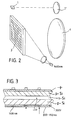
- Fig. 2 shows as a detail of the overall system a CCD array 3 with receiving optics 4, in which, in contrast to Fig. 1, a controllable closure 5 in gating design was made for the conventional CCD semiconductor element arrangement, e.g.
- a semiconductor laser can be used here with a gating wavelength ⁇ 2 for driving between preferably 1400 nm to about 1800 nm. It is important that this driving wavelength can be sufficiently differentiated from the measuring wavelength ⁇ 1 of the incident light, in particular 800-950 nm, as it does is used in semiconductor lasers for distance measurement.
- the control of the semiconductor laser for the gating is shown in one exemplary embodiment in FIG. 8.
- An embodiment and application is shown geometrically in FIG. 3, in particular for the aforementioned optical shutter, such as exposure control.
- the layer sequence of the structure is p-n-p.
- the irradiation onto the bottom layer in FIG. 3 takes place from below and a voltage of up to approximately -300 V is applied, a voltage of approximately + 5 V is applied to the n-layer formed in the central region, while the voltage in FIG. 3 top structure is used for reading.
- the incident radiation can then, as in the drawing in FIG. 3 It can be seen that after the voltage has been applied, it can be controlled and then, if necessary, readable on electrodes, as described, for example, in DE 38 17 153 A1 or according to the block diagram according to FIG. 9.
- Fig. 4 the design is such that the avalanche effect is not exploited on the back of the radiation as in Fig. 3, but on the contrary, on the side, i.e. in Fig. 4 is done horizontally side by side.
- a high-resistance nSi layer and a CCD structure are deposited on a transparent or semi-transparent substrate in the central region seen horizontally and in cross section.
- Fig. 4 from above is conical down in continuous areas in particular transparent SiO2 over pSi and between nSi in the bottom layer on the substrate.
- the CCD structure is applied from pSi over the readout structure arranged on the right in FIG. 4, in particular electrode structure such as aluminum electrodes or the like.
- the incident radiation for gating or driving with the wavelength ⁇ 2 is different from this, it also being possible for a filter layer to be arranged above the SiO2.
- FIG. 5 A further embodiment of an optically controllable image sensor can be seen in FIG. 5.
- This in turn is an individual representation of a semiconducting element in cross section, the structure and the sequence of layers being clear.
- PSi is applied over a gold layer that emits the radiation side for the image information, in FIG. 5 below.
- nSi with a very high resistance
- pSi again by pSi. 3
- SiO2 or the like material is arranged laterally spaced between individual pSi regions in the lower pSi layer.
- the arrangement is advantageously made such that the radiation for the image information is not vertically below the direction of incidence of the control light, but side by side.
- the control light from the pulsating laser in FIG. 5 is irradiated from the top in order to generate a space charge in the semiconductor element.
- a different voltage in relation to the pSi layer is in turn applied to the nSi layer.
- a transparent or semi-transparent layer, preferably made of SiO2 is applied to the top of the pSi layer. is applied in the form of parallel tracks (see. DE 38 17 153 A1).
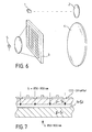
- FIG. 6 Another embodiment is shown in Fig. 6.
- the image evaluation in the receiving section can be designed differently and can be used with particular advantage for automatic vehicle guidance at a mutual, predetermined distance (in the convoy) see "Funkschau" 14/1988 page 42 pp.
- a scanning laser is used in the receiving part with transmitting optics and receiving optics, which is arranged on the side of the CCD array which is turned away when the radiation to be measured is incident.
- the transmitter laser can in turn generate 800-900 nm measuring wavelength for the scene lighting with the aid of the transmitting optics or another measuring wavelength ⁇ 1, which is suitable for imaging and automatic steering or guidance of a vehicle.
- FIG. 7 A cross section through the CCD element to FIG. 6 is shown in FIG. 7, the basic structure again being the p-n-p sequence.
- the incident radiation comes from above and the metal readout electrodes are also arranged at the top in this embodiment and are applied using mask technology, in particular by photolithography.
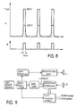
- FIG. 8 shows a signal sequence which is given here for a better understanding of the function.
- the radiation ⁇ to be measured is applied at an illuminance of up to approximately 10000lux, a voltage of up to approximately 300V negative voltage is applied in order to carry out the optical control of the image sensor (gating).
- the current flow ⁇ is shown and the scanning of the scanning laser over time.
- the key pulses are e.g. in the range of 10 ns and less.
- suitable other keying or clocking or pulse sequences or modulation are possible (e.g. pulse code modulation or pulse duration modulation).
- FIG. 9 shows a block diagram of the overall system in use for vehicles as described above. The details can be found in the respective function blocks, as can the overall switching arrangement.
- an areal image sensor was created with on the one hand high sensitivity and on the other hand the possibility to control it in a very short predetermined time, in the nano-second range, in particular ⁇ 10 ns (here e.g. approx. 5ns).
- the sensitivity is increased by a factor of 100 thanks to the special way in which the avalanche effect is used.
- the gain factor can be set using the avalanche voltage.
- the application of the invention is advantageous in the case of a distance warning system and distance system using a laser according to DE 36 40 449 A1.
Landscapes
- Engineering & Computer Science (AREA)
- Physics & Mathematics (AREA)
- Computer Networks & Wireless Communication (AREA)
- General Physics & Mathematics (AREA)
- Radar, Positioning & Navigation (AREA)
- Remote Sensing (AREA)
- Electromagnetism (AREA)
- Optical Radar Systems And Details Thereof (AREA)
- Solid State Image Pick-Up Elements (AREA)
- Transforming Light Signals Into Electric Signals (AREA)
Abstract
Description
- Die Erfindung betrifft einen Bildsensor gemäß dem Oberbegriff des Patentanspruchs 1.
- Es sind Bildsensoren auf der Basis von Halbleiterelementen vielfach bekannt. Ein Übersichtsartikel ist z.B. in Elektronik-Praxis Nr. 9 September 1978 Seiten 12 ff. enthalten. Es handelt sich bei den Bildsensoren um Schaltungen, bei denen höchste Integrationsfähigkeit wichtig ist und bei der deshalb große Anforderungen an die Herstellungstechnologie zu stellen sind. Dies gilt insbesondere dann wenn die Ausgangssignale, die in dem Sensor z.B. nach Einfallen einer Strahlung abgegeben werden können, nur sehr klein sind.
- Aufgabe der Erfindung ist es, einen Bildsensor zu schaffen auf Halbleiterbasis, der eine wesentlich höhere Ausbeute (Signal-Rauschabstand) bzw. ein gesteigertes Nutzsignal erbringt und auf einfache Weise steuerbar ist.
- Gelöst wird diese Aufgabe durch einen Bildsensor, dessen fotoempfindliches Element auf Halbleiterbasis, wie CCD-Element oder Elementenanordnung, durch Erzeugen eines Avalanche-Effektes in einer Schicht optisch steuerbar ist.
Durch die Ausnützung des Avalanche-Effektes bzw. einer flächenhaften Avalanche-Diode an einem CCD-Sensor wird eine Empfindlichkeitserhöhung des Sensorelementes um das 100-fache erreicht. - Weitere Merkmale und Vorteile der Erfindung sind den weiteren Ansprüchen, sowie der Beschreibung und Zeichnung von Ausführungsbeispielen zu entnehmen.
- Es zeigen:
- Fig. 1 den Aufbau des optischen Gesamtsystems in einer ersten Anwendung,
- Fig. 2 einen optischen Empfänger einer ersten Art,
- Fig. 3 ein Empfangselement (CCD-Element) zu Fig. 2,
- Fig. 4 ein Empfangselement anderer Art, abgewandelt gegenüber Fig. 3,
- Fig. 5 ein CCD-Element weiter abgewandelter Art,
- Fig. 6 ein Empfänger zu Fig. 5,
- Fig. 7 eine Anordnung zu Fig. 6 im Querschnitt,
- Fig. 8 ein Diagramm von Signalfolgen zu einem Element nach Fig. 7,
- Fig. 9 ein Blockschaltbild für einen optisch steuerbaren Bildsensor und eine Anwendung hierfür.
- Die Erfindung wird nachstehend anhand von Ausführungsbeispielen erläutert ohne hierauf beschränkt zu sein. Sie umfaßt selbstverständlich auch Abwandlungen und Kombinationen von beanspruchten, beschriebenen und dargestellten Merkmalen.
- Wie Fig.1 zeigt, läßt sich ein Bildsensor flächenhafter Ausführung in Halbleiterbauweise als CCD-Array so gestalten, daß er zusammen mit einer Empfangsoptik den Empfänger des Systems bildet, während ein Laser-Sender und eine Sendeoptik die optische Strahlung aussenden, die empfangen wird, um Abbildungen z.B. auf einer Straße vorausblickend von einem Kraftfahrzeug aus zu erlangen, bei dem ebenfalls Laser-Strahlen zur Abstandsmessung zu Hindernissen und/oder vorausfahrenden Fahrzeugen ausgesendet, empfangen und ausgewertet werden.
- Der Sender ist mit 1, die Sendeoptik mit 2, der Empfänger als CCD-Array 3 ausgebildet und die Empfangsoptik mit 4 bezeichnet. Eine Abbildung wie vom Sensor gewonnen ist direkt unter diesem verkleinert dargestellt. Die Auswerteschaltung und Auswertemittel sind an sich bekannter Art und deshalb nicht dargestellt und auch nicht näher erläutert.
- Neu und erfindungswesentlich ist, daß auf einer Fläche des CCD-Sensors auf der Rückseite des Halbleiters in den Strahlung einfällt, eine Avalanche-Diode aufgebracht ist. Dies wird durch Implantieren einer geeigneten Beschichtung auf der Rückseite des CCD-Chips erreicht. Die Herstellungstechnologie kann auf verschiedene Weise ausgeführt werden. Die Materialien zum Implantieren bzw. Dotieren sind ebenfalls bekannter Art.
- Fig. 2 zeigt als Detail des Gesamtsystems ein CCD-Array 3 mit Empfangsoptik 4 wobei von Fig.1 abweichend ein steuerbarer Verschluß 5 in Gating-Ausführung für die herkömmliche CCD-Halbleiterelementanordnung getroffen wurde, z.B. kann ein Halbleiter-Laser hier verwendet werden mit einer Gating-Wellenlänge λ2 zum Ansteuern zwischen bevorzugt 1400 nm bis etwa 1800 nm. Wichtig ist, daß diese Ansteuerwellenlänge ausreichend unterschieden werden kann von der Meßwellenlänge λ1 des einfallenden Lichtes insbesondere 800 - 950 nm, wie sie bei Halbleiter-Lasern zum Entfernungsmessen angewandt wird.
- Die Ansteuerung des Halbleiter-Lasers für das Gating ist in einem Ausführungsbeispiel in Fig. 8 gezeigt. Geometrisch ist eine Ausführung und Anwendung in Fig. 3 gezeigt, insbesondere für den genannten optischen Verschluß, wie Belichtungssteuerung. Dabei ist die Schichtfolge des Aufbaus p-n-p.
- Auf die in Fig. 3 unterste Schicht erfolgt die Einstrahlung in dieser Darstellung von unten und es wird eine Spannung von bis etwa -300V angelegt, an die im mittleren Bereich ausgebildete n-Schicht eine Spannung von etwa + 5 V, während die in Fig. 3 oberste Struktur zum Auslesen dient. Die einfallende Strahlung kann dann wie in der Zeichnung Fig. 3 ersichtlich nach Anlegen der Spannung durchsteuerbar sein und dann ggfs. an Elektroden auslesbar sein, wie z.B. in der DE 38 17 153 A1 beschrieben oder gemäß dem Blockschaltbild nach Fig. 9.
- In Fig. 4 ist die Ausführung so getroffen, daß nicht auf der Rückseite des Strahlungseinfalls die Ausnutzung des Avalanche-Effektes wie in Fig. 3 erfolgt, sondern im Gegenteil seitlich d.h. in Fig. 4 horizontal nebeneinander erfolgt. Dabei ist auf einem transparentem oder semitransparenten Substrat eine hochohmige nSi-Schicht und darauf eine CCD-Struktur im horizontal und im Querschnitt gesehenen mittigen Bereich abgeschieden. In Fig. 4 von oben aus ist kegelförmig nach unten in durchgehenden Bereichen insbesondere transparentes SiO₂ über pSi und zwischen nSi in der untersten Schicht auf dem Substrat eingebettet. Die CCD-Struktur ist aus pSi über der in Fig. 4 rechts angeordneten Auslesestruktur, insbesondere Elektrodenstruktur wie Aluminium-Elektroden o.ä., aufgebracht.
- Auf der in Fig. 4 linken Seite ist eine dünne Schicht aus transparentem Werkstoff, wie Gold, aufgebracht und bevorzugt eine oder mehrere Filterschichten für die zu messende einfallende Strahlung insbesondere ein Licht/Bild mit der Wellenlänge λ1. Hiervon verschieden ist die einfallende Strahlung für das Gating bzw. Ansteuern mit der Wellenlänge λ2, wobei ebenfalls über dem SiO₂ noch eine Filterschicht angeordnet sein kann.
- Eine weitere Ausführung eines optisch steuerbaren Bildsensors ist in Fig. 5 ersichtlich. Es handelt sich hierbei wiederum um eine Einzeldarstellung eines halbleitenden Elementes im Querschnitt, wobei der Aufbau und die Schichtenfolge deutlich wird. Über eine Goldschicht die die Einstrahlungsseite für die Bildinformation abgibt, in Fig. 5 unten, ist pSi aufgebracht. Hierüber folgt wieder nSi sehr hochohmig und darauf wieder pSi. Abweichend gegenüber Fig. 3 ist jedoch in der unteren pSi-Schicht SiO₂ oder dergleichen Material zwischen einzelnen pSi-Bereichen jeweils lateral beabstandet angeordnet.
- Die Anordnung ist mit Vorteil so getroffen, daß die Einstrahlung für die Bildinformation nicht vertikal unterhalb der Einfallsrichtung des Steuerlichtes liegt, sondern seitlich nebeneinander. Anders als bei der Ausführung nach Fig. 3 erfolgt das Einstrahlen des Steuerlichts von dem pulsierenden Laser in Fig. 5 von der Oberseite her, um eine Raumladung in dem Halbleiterelement zu erzeugen. An die nSi-Schicht ist wiederum eine unterschiedliche Spannung im Verhältnis zur pSi-Schicht angelegt. Auf der Oberseite ist über der pSi-Schicht eine transparente oder semi-transparente Schicht bevorzugt aus SiO₂ aufgebracht, auf der in Maskentechnik, insbesondere nach fotolithographischem Verfahren, die Ausleseelektronenstruktur insbesondere mit Aluminium- oder Goldelektroden o.ä. in Form von Parallel-Bahnen aufgebracht ist (vgl. DE 38 17 153 A1).
- Eine andere Ausführung ist in Fig. 6 dargestellt. Hier kann die Bildauswertung im Empfangsteil anders gestaltet sein und insbesondere für eine automatische Fahrzeugführung in gegenseitigem, vorbestimmtem Abstand (im Convoy) siehe "Funkschau" 14/1988 Seite 42 pp, mit Vorteil angewandt werden. Dabei wird im Empfangsteil mit Sendeoptik und Empfangsoptik ein Abtastlaser verwandt, der auf der bei Strahlungseinfall der zu messenden Strahlung abgekehrten Seite des CCD-Arrays angeordnet ist. Der Sendelaser kann für die Szenenbeleuchtung wiederum 800-900 nm Meßwellenlänge mit Hilfe der Sendeoptik erzeugen oder einer anderen Meßwellenlänge λ1, die für die Abbildung und automatischer Lenkung bzw. Führung eines Fahrzeugs geeignet ist. Ein Querschnitt durch das CCD-Element zu Fig. 6 ist in Fig. 7 dargestellt, wobei der Grundaufbau wiederum die p-n-p-Folge ist. Die einfallende Strahlung kommt in Fig. 7 von oben und die Metallausleseelektroden sind bei dieser Ausführung ebenfalls oben angeordnet und in Maskentechnik insbesondere auf photolithographischem Wege aufgebracht.
- In Fig. 8 ist eine Signalfolge dargestellt, die zum besseren Verständnis der Funktion hier angeführt ist. Im oberen Teil ist die zumessende Strahlung ε aufgetragen bei einer Beleuchtungsstärke bis etwa 10000lux wird eine Spannung angelegt bis zu etwa 300V negativer Spannung, um die optische Steuerung des Bildsensors (Gating) durchzuführen.
- Im unteren Teil des Diagramms ist der Stromfluß φ dargestellt und die zeitliche Tastung des Abtastlasers. Die Tastimpulse liegen z.B. im Bereich von 10 ns und kleiner. Selbstverständlich sind geeignete andere Tastungen oder Taktungen oder Pulsfolgen oder Modulation möglich (z.B. Pulscodemodula- tion oder Pulsdauermodulation).
- In Fig. 9 ist ein Blockschaltbild des Gesamtsystems in der Anwendung für Fahrzeuge wie vorbeschrieben dargestellt. Die Einzelheiten sind den jeweiligen Funktionsblöcken zu entnehmen, ebenso die Gesamtschaltanordnung.
- Aus vorstehendem wird deutlich, daß ein flächenhafter Bildsensor geschaffen wurde mit einerseits hoher Empfindlichkeit und andererseits der Möglichkeit diesen in sehr kurzer vorgegebener Zeit zu steuern, im Nano-Sek.-Bereich, insbesondere < 10 ns (hier z.B. ca. 5ns). Damit ist ein elektrischer Verschluß für eine CCD-Kamera geschaffen, die auch in Fahrzeugen anwendbar ist. Die Empfindlichkeitserhöhung um den Faktor 100, ist dank der besonderen Weise der Ausnutzung des Avalanche-Effekts gegeben. Der Verstärkungsfaktor ist mit Hilfe der Avalanche-Spannung einstellbar.
- Die Anwendung der Erfindung ist bei einem Abstandswarnsystem und Entfernungssystem mittels Laser nach DE 36 40 449 A1 von Vorteil.
- Die Anwendung bei einem automatischen Führungssystem "Prometheus" vgl. Bild der Wissenschaft 10 - 1988, S. 134 ist besonders vorteilhaft.
Claims (4)
- auf der einen Seite des Halbleiters eine Avalanchediode angeordnet ist,
- durch die ein bei Lichteinfall von außen erzeugter Photostrom verstärkt wird,
- eine Raumladung im anschließenden Halbleitergebiet erzeugt wird und ein Ladungsträgertransport zur CCD-Auslesestruktur hin erfolgt,
- in der auf der anderen Seite des Halbleiters angeordneten CCD-Auslesestruktur ein Kontrast- oder Entfernungsbild ausgegeben wird,
- daß er durch Einleiten gepulsten Lichtes in das Halbleitergebiet in dem die Raumladung erzeugt wurde, optisch steuerbar ist.
Applications Claiming Priority (2)
| Application Number | Priority Date | Filing Date | Title |
|---|---|---|---|
| DE3839512 | 1988-11-23 | ||
| DE3839512A DE3839512A1 (de) | 1988-11-23 | 1988-11-23 | Bildsensor |
Publications (3)
| Publication Number | Publication Date |
|---|---|
| EP0371197A2 true EP0371197A2 (de) | 1990-06-06 |
| EP0371197A3 EP0371197A3 (en) | 1990-11-28 |
| EP0371197B1 EP0371197B1 (de) | 1994-12-21 |
Family
ID=6367705
Family Applications (1)
| Application Number | Title | Priority Date | Filing Date |
|---|---|---|---|
| EP89112924A Expired - Lifetime EP0371197B1 (de) | 1988-11-23 | 1989-07-14 | Bildsensor |
Country Status (5)
| Country | Link |
|---|---|
| US (1) | US5005085A (de) |
| EP (1) | EP0371197B1 (de) |
| JP (1) | JP2540213B2 (de) |
| CA (1) | CA2003683A1 (de) |
| DE (1) | DE58908801D1 (de) |
Families Citing this family (8)
| Publication number | Priority date | Publication date | Assignee | Title |
|---|---|---|---|---|
| FR2676284B1 (fr) * | 1991-05-07 | 1994-12-02 | Peugeot | Procede de detection d'obstacles presents devant un vehicule automobile et dispositif pour la mise en óoeuvre d'un tel procede. |
| FR2682186B1 (fr) * | 1991-10-08 | 1993-12-03 | Thomson Csf | Detecteur infrarouge a haute sensibilite et camera infrarouge utilisant un tel detecteur. |
| DE4436447C2 (de) * | 1994-10-13 | 1996-10-02 | Leica Ag | Verfahren und Vorrichtung zur elektrooptischen Entfernungsmessung |
| DE4440613C1 (de) * | 1994-11-14 | 1996-07-25 | Leica Ag | Vorrichtung und Verfahren zur Detektion und Demodulation eines intensitätsmodulierten Strahlungsfeldes |
| US5821547A (en) * | 1997-03-10 | 1998-10-13 | Talmi; Yair | Temporal filter using interline charged coupled device |
| US6961092B1 (en) * | 1999-07-30 | 2005-11-01 | Pentax Corporation | Three-dimensional image capturing device |
| US6618125B2 (en) * | 2000-09-05 | 2003-09-09 | The United States Of America As Represented By The Secretary Of The Army | Code-multiplexed read-out for ladar systems |
| CN107092041A (zh) * | 2017-03-01 | 2017-08-25 | 江西理工大学 | 一种激光告警器 |
Family Cites Families (10)
| Publication number | Priority date | Publication date | Assignee | Title |
|---|---|---|---|---|
| JPS59131282A (ja) * | 1983-01-17 | 1984-07-28 | Mitsubishi Electric Corp | 自動車用後方監視装置 |
| JPS59198754A (ja) * | 1983-04-26 | 1984-11-10 | Toshiba Corp | カラ−用固体撮像デバイス |
| JPH0799868B2 (ja) * | 1984-12-26 | 1995-10-25 | 日本放送協会 | 固体撮像装置 |
| JPS62261931A (ja) * | 1986-05-09 | 1987-11-14 | Hitachi Ltd | 受光素子 |
| NL8602091A (nl) * | 1986-08-18 | 1988-03-16 | Philips Nv | Beeldopneeminrichting uitgevoerd met een vaste-stof beeldopnemer en een elektronische sluiter. |
| DE3640449C1 (de) * | 1986-11-27 | 1988-06-30 | Messerschmitt Boelkow Blohm | Einrichtung zum Bestimmen der Entfernung zwischen zwei Objekten,insbesondere zwei Kraftfahrzeugen |
| FR2612334B1 (fr) * | 1986-12-12 | 1989-04-21 | Thomson Csf | Dispositif de multiplication de porteurs de charge par un phenomene d'avalanche et son application aux photodetecteurs, aux photocathodes, et aux visionneurs infrarouges |
| JPH0715979B2 (ja) * | 1987-08-27 | 1995-02-22 | 三菱電機株式会社 | 超格子撮像素子 |
| DE3732347C1 (de) * | 1987-09-25 | 1989-03-16 | Messerschmitt Boelkow Blohm | Entfernungsbild-Sensor |
| DE3817153A1 (de) * | 1988-05-19 | 1989-11-30 | Messerschmitt Boelkow Blohm | Halbleiter-bauelement |
-
1989
- 1989-07-14 EP EP89112924A patent/EP0371197B1/de not_active Expired - Lifetime
- 1989-07-14 DE DE58908801T patent/DE58908801D1/de not_active Expired - Lifetime
- 1989-08-29 JP JP1220496A patent/JP2540213B2/ja not_active Expired - Fee Related
- 1989-11-22 US US07/440,601 patent/US5005085A/en not_active Expired - Lifetime
- 1989-11-23 CA CA002003683A patent/CA2003683A1/en not_active Abandoned
Also Published As
| Publication number | Publication date |
|---|---|
| EP0371197A3 (en) | 1990-11-28 |
| DE58908801D1 (de) | 1995-02-02 |
| JP2540213B2 (ja) | 1996-10-02 |
| EP0371197B1 (de) | 1994-12-21 |
| US5005085A (en) | 1991-04-02 |
| CA2003683A1 (en) | 1990-05-23 |
| JPH02214275A (ja) | 1990-08-27 |
Similar Documents
| Publication | Publication Date | Title |
|---|---|---|
| DE2920950C2 (de) | ||
| DE3839513C2 (de) | ||
| EP1009984A1 (de) | Verfahren und vorrichtung zur bestimmung der phasen- und/oder amplitudeninformation einer elektromagnetischen welle | |
| DE2912884A1 (de) | Photomessfuehlereinrichtung und diese verwendendes bildabtastsystem | |
| DE19859670A1 (de) | Abtastkopf und Verfahren zu dessen Herstellung | |
| DE2920951A1 (de) | Entfernungsmesseinrichtung | |
| DE3122187A1 (de) | Entfernungsmesseinrichtung | |
| DE212017000247U1 (de) | LiDAR-Vorrichtung | |
| DE102019103721A1 (de) | Bildsensor zum Erfassen von LED-Licht mit reduziertem Flimmern | |
| DE3839512A1 (de) | Bildsensor | |
| EP0371197B1 (de) | Bildsensor | |
| DE2944161C2 (de) | Vorrichtung zur Feststellung der Scharfeinstellung eines optischen Systems | |
| DE2263616C3 (de) | Automatische Fokussiereinrichtung | |
| DE19949838A1 (de) | Entfernungsmeßeinrichtung | |
| DE3317090A1 (de) | Fokusdetektor | |
| DE19946449A1 (de) | Entfernungsmeßeinrichtung | |
| DE3634503C2 (de) | Automatische Entfernungsmeßvorrichtung | |
| DE3241600C2 (de) | Automatische Scharfeinstellvorrichtung für Kameraobjektive | |
| DE3840425A1 (de) | Entfernungsbild-sensor | |
| DE19946448B4 (de) | Entfernungsmeßeinrichtung | |
| DE2636769B1 (de) | Vorrichtung zur messung der geschwindigkeit und/oder der bewegungsrichtung einer bildstruktur | |
| DE3840426A1 (de) | Entfernungsbild-sensor | |
| DE2801495B2 (de) | Vorrichtung zur Erzeugung eines oder mehrerer Bildsignale, die eine Information Über die Bildschärfe eines Bildes oder über die Lagedifferenz zwischen zwei Bildern enthalten | |
| WO2018086813A1 (de) | Tof-kamera, kraftfahrzeug, verfahren zum herstellen einer tof-kamera und verfahren zum ermitteln eines abstands zu einem objekt | |
| DE69208739T2 (de) | Mehrpunkt-Entfernungsmesser |
Legal Events
| Date | Code | Title | Description |
|---|---|---|---|
| PUAI | Public reference made under article 153(3) epc to a published international application that has entered the european phase |
Free format text: ORIGINAL CODE: 0009012 |
|
| AK | Designated contracting states |
Kind code of ref document: A2 Designated state(s): DE FR GB IT SE |
|
| PUAL | Search report despatched |
Free format text: ORIGINAL CODE: 0009013 |
|
| AK | Designated contracting states |
Kind code of ref document: A3 Designated state(s): DE FR GB IT SE |
|
| 17P | Request for examination filed |
Effective date: 19901117 |
|
| RAP1 | Party data changed (applicant data changed or rights of an application transferred) |
Owner name: DEUTSCHE AEROSPACE AKTIENGESELLSCHAFT |
|
| 17Q | First examination report despatched |
Effective date: 19930518 |
|
| RAP1 | Party data changed (applicant data changed or rights of an application transferred) |
Owner name: TEMIC TELEFUNKEN MICROELECTRONIC GMBH |
|
| GRAA | (expected) grant |
Free format text: ORIGINAL CODE: 0009210 |
|
| AK | Designated contracting states |
Kind code of ref document: B1 Designated state(s): DE FR GB IT SE |
|
| ITF | It: translation for a ep patent filed | ||
| REF | Corresponds to: |
Ref document number: 58908801 Country of ref document: DE Date of ref document: 19950202 |
|
| GBT | Gb: translation of ep patent filed (gb section 77(6)(a)/1977) |
Effective date: 19950117 |
|
| ET | Fr: translation filed | ||
| PLBE | No opposition filed within time limit |
Free format text: ORIGINAL CODE: 0009261 |
|
| STAA | Information on the status of an ep patent application or granted ep patent |
Free format text: STATUS: NO OPPOSITION FILED WITHIN TIME LIMIT |
|
| 26N | No opposition filed | ||
| REG | Reference to a national code |
Ref country code: GB Ref legal event code: IF02 |
|
| PGFP | Annual fee paid to national office [announced via postgrant information from national office to epo] |
Ref country code: GB Payment date: 20030704 Year of fee payment: 15 |
|
| PGFP | Annual fee paid to national office [announced via postgrant information from national office to epo] |
Ref country code: SE Payment date: 20030708 Year of fee payment: 15 |
|
| PGFP | Annual fee paid to national office [announced via postgrant information from national office to epo] |
Ref country code: FR Payment date: 20040708 Year of fee payment: 16 |
|
| PG25 | Lapsed in a contracting state [announced via postgrant information from national office to epo] |
Ref country code: GB Free format text: LAPSE BECAUSE OF NON-PAYMENT OF DUE FEES Effective date: 20040714 |
|
| PG25 | Lapsed in a contracting state [announced via postgrant information from national office to epo] |
Ref country code: SE Free format text: LAPSE BECAUSE OF NON-PAYMENT OF DUE FEES Effective date: 20040715 |
|
| EUG | Se: european patent has lapsed | ||
| GBPC | Gb: european patent ceased through non-payment of renewal fee |
Effective date: 20040714 |
|
| PG25 | Lapsed in a contracting state [announced via postgrant information from national office to epo] |
Ref country code: IT Free format text: LAPSE BECAUSE OF NON-PAYMENT OF DUE FEES;WARNING: LAPSES OF ITALIAN PATENTS WITH EFFECTIVE DATE BEFORE 2007 MAY HAVE OCCURRED AT ANY TIME BEFORE 2007. THE CORRECT EFFECTIVE DATE MAY BE DIFFERENT FROM THE ONE RECORDED. Effective date: 20050714 |
|
| PG25 | Lapsed in a contracting state [announced via postgrant information from national office to epo] |
Ref country code: FR Free format text: LAPSE BECAUSE OF NON-PAYMENT OF DUE FEES Effective date: 20060331 |
|
| REG | Reference to a national code |
Ref country code: FR Ref legal event code: ST Effective date: 20060331 |
|
| PGFP | Annual fee paid to national office [announced via postgrant information from national office to epo] |
Ref country code: DE Payment date: 20080811 Year of fee payment: 20 |