EP0371418A2 - Dispositif et procédé de disposition du compteur de programme d'un microprocesseur à l'extérieur de l'appareil - Google Patents
Dispositif et procédé de disposition du compteur de programme d'un microprocesseur à l'extérieur de l'appareil Download PDFInfo
- Publication number
- EP0371418A2 EP0371418A2 EP89121797A EP89121797A EP0371418A2 EP 0371418 A2 EP0371418 A2 EP 0371418A2 EP 89121797 A EP89121797 A EP 89121797A EP 89121797 A EP89121797 A EP 89121797A EP 0371418 A2 EP0371418 A2 EP 0371418A2
- Authority
- EP
- European Patent Office
- Prior art keywords
- instruction
- bus
- program
- address
- external
- Prior art date
- Legal status (The legal status is an assumption and is not a legal conclusion. Google has not performed a legal analysis and makes no representation as to the accuracy of the status listed.)
- Withdrawn
Links
Images

Classifications
-
- G—PHYSICS
- G06—COMPUTING OR CALCULATING; COUNTING
- G06F—ELECTRIC DIGITAL DATA PROCESSING
- G06F11/00—Error detection; Error correction; Monitoring
- G06F11/36—Prevention of errors by analysis, debugging or testing of software
- G06F11/362—Debugging of software
- G06F11/3636—Debugging of software by tracing the execution of the program
-
- G—PHYSICS
- G06—COMPUTING OR CALCULATING; COUNTING
- G06F—ELECTRIC DIGITAL DATA PROCESSING
- G06F11/00—Error detection; Error correction; Monitoring
- G06F11/30—Monitoring
- G06F11/34—Recording or statistical evaluation of computer activity, e.g. of down time, of input/output operation ; Recording or statistical evaluation of user activity, e.g. usability assessment
-
- G—PHYSICS
- G06—COMPUTING OR CALCULATING; COUNTING
- G06F—ELECTRIC DIGITAL DATA PROCESSING
- G06F11/00—Error detection; Error correction; Monitoring
- G06F11/36—Prevention of errors by analysis, debugging or testing of software
- G06F11/362—Debugging of software
- G06F11/3648—Debugging of software using additional hardware
- G06F11/3656—Debugging of software using additional hardware using a specific debug interface
Definitions
- the present invention relates to in-circuit emulation and, in particular, to a technique for providing a microprocessor's program counter value external to the device on a dedicated bus so that an emulator can readily generate a list of executed instruction addresses by monitoring this bus.
- a microprocessor is useful only if it is possible for systems designers incorporating the microprocessor to "debug" their systems.
- One particular challenge of developing a microprocessor system design is to identify "bugs" that arise only rarely or only at full frequency operation.
- Microprocessor system designers rely on so-called in-circuit emulation techniques to monitor a working system and trace information relating to the ongoing operation of the system to diagnose bugs.
- One of the most important elements of information to be traced is the value contained in the microprocessor's program counter register.
- a microprocessor's program counter register contains the address of the instruction that is presently being executed by the microprocessor. Therefore, by tracing the address value contained in the program counter register, the sequence of instruction execution in the program operating the system can be monitored.
- the conventional approach to tracing program execution has been a three step process.
- traffic on the system bus is monitored to trace instruction and data transfers between the system's processing unit and remote main memory.
- instruction read references are extracted from the bus traffic.
- the probable sequence of instruction execution is reconstructed based on the extracted instruction read references.
- the prior art technique for solving this problem is to design an external discrete implementation of portions of the particular microprocessor to be emulated. This permits instruction address reconstruction from system bus traffic and from key signals provided by discrete hardware in the emulator.
- An additional emulation problem has been correlating the trace listing of executed instructions with a program listing, since the program listing consists of virtual addresses, while the trace listing consists of physical addresses.
- the difference is due to address translation at run time performed by a memory management unit.
- the processing unit's integrated memory management unit translates the virtual addresses generated by the executing program to the physical addresses used to access main memory via the system bus. In some circumstances, this translation will not be 1:1; that is, more than one virtual address can be translated to a single physical address. In such cases, it is impossible to determine the virtual addresses of memory references for an executing program by merely observing the physical addresses of the instruction read references on the system bus. Thus, the task of translating addresses from physical back to virtual is not normally possible because of insufficient information available to the emulator. When this translation is important, an external MMU-like device must be built with discrete or custom hardware to provide this functionality in the emulator.
- the present invention addresses all of the above-described current problems associated with in-circuit emulation by providing a microprocessor's program counter value external to the device on a dedicated bus.
- An emulator can then readily generate a list of executed instruction addresses by simply monitoring this bus. This eliminates the conventional requirement of monitoring system bus traffic and attempting to extract and reconstruct the sequence of instruction execution. Since the externally-provided program counter value is synchronized with the internal program counter of the microprocessor, there is no latency between the observed program counter value and the actual program counter value. Furthermore, the addresses of all executed instructions are observable on the external pins. Therefore, it is not necessary to degrade processor performance by disabling an instruction cache, nor is it necessary to build address translation hardware for converting physical addresses back to virtual addresses.
- Fig. 1 shows a microprocessor 10 that is organized internally as eight major functional units.
- a loader 12 prefetches instructions and decodes them for use by an address unit 14 and an execution unit 16.
- Loader 12 receives code characters from an instruction cache 18 in the form of 32-bit doublewords and aligns the code characters as the corresponding instructions.
- Loader 12 transfers instructions received from instruction cache 18 into an 8-byte instruction queue.
- Loader 12 can extract an instruction field on each cycle, where a "field" means either an op code, displacement or immediate value.
- Loader 12 decodes the op code to generate the initial microcode address, which is passed on to execution unit 16.
- the decoded general addressing codes are passed on the ADMS bus to address unit 14.
- Displacement values are passed to address unit 14 on the DISP bus.
- Address unit 14 calculates effective addresses using a dedicated 32-bit adder and reads source operands for execution unit 16. Address unit 14 controls a port from a register file 20 to the GCBUS through which it transfers base and index values to the address adder and data values to execution unit 16. Effective addresses for operand references are transferred to memory management unit 22 and data cache 26 on the GVA bus, which is the virtual address bus.
- Execution unit 16 includes the data path and the microcoded control for executing instructions and processing exceptions.
- Execution unit 16 controls a port to register file 20 from the GNA bus on which it stores results.
- the GNA bus is also used by execution unit 16 to read the values of dedicated registers.
- a two-entry data buffer allows execution unit 16 to overlap the execution of one instruction with storing results to memory for previous instructions.
- the GVA bus is used by execution unit 16 to perform memory references for complex instructions and exception processing.
- a 32-bit program counter register 28 which holds the virtual address of the currently executing instruction, is among the dedicated registers of microprocessor 10.
- the instruction cache 18, address unit 14 and execution unit 16 make requests to memory management unit 22 via the GVA bus for references to external main memory.
- Memory management unit 22 arbitrates the requests, granting access to transfer a virtual address on the GVA bus.
- Memory management unit 22 translates the virtual address it receives on the GVA bus to the corresponding physical address using its local translation buffer 22a.
- Instruction cache 18 includes an instruction buffer from which it can transfer 32 bits of code per cycle on the IBUS to loader 12. If the instruction read reference results in an instruction cache hit, then the instruction buffer is loaded from the selected set of instruction cache 18. In the event of a miss, instruction cache 18 transfers the address of the missing instruction on the GVA bus to memory management unit 22 which translates the virtual address to its corresponding physical address for an external reference by bus interface unit 24. Bus interface unit 24 then initiates a read cycle to load the instruction buffer from external memory via the GBDI bus. The reference instruction is then written to one of the sets of instruction cache 18.
- memory management unit 22 When a data read reference is issued, memory management unit 22 translates the virtual address to the corresponding physical address and transfers it to data cache 26 and bus interface unit 24 on the MPA bus. Data cache 26 performs address comparison while bus interface unit 24 simultaneously initiates a bus cycle to read data from external memory. If the cache reference is a hit, then the selected data is transferred fron data cache 26 to execution unit 16 on the GDATA bus and bus interface unit 24 cancels the external bus cycle. If the reference is a miss, the bus interface unit 24 completes the external bus cycle and transfers data from external memory to execution unit 16 and data cache 26 which updates the cache entry.
- microprocessor 10 automatically locates the information in external memory and updates the translation buffer 22a.
- the program counter register 28 of microprocessor 10 contains the virtual address of the first byte of the instruction currently being executed by microprocessor 10. The address value contained in the program counter register 28 is incremented to point to the next instruction only when microprocessor 10 completes execution of the current instruction.
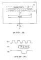
- microprocessor 10 provides the value of the virtual program counter register 28 for each executed instruction. This value is available via a dedicated 16-bit external bus 30 which, as shown in Fig. 3, provides this information on two consecutive cycles synchronized to active low program fetch status (PFS). If sufficient external pins are available, the full 32-bit value can be made available in a single cycle.
- the program counter value is made available on the bus 30 without affecting performance, thus ensuring that microprocessors that are intended for in-circuit emulation will be identical in behavior to other microprocessors.
- microprocessor 10 Whenever a new instruction begins actual execution, microprocessor 10 activates the PFS signal. As stated above, the 32-bit virtual program counter register value of that instruction is sent out on the 16-bit bus 30 in two consecutive cycles, beginning with the lower 16 bits.
- microprocessor 10 will trap via its conventional trap mechanism.
- the next virtual program counter value to be sent out on the bus 30 in synchronization to the next PFS signal will be that of the first instruction of the trap routine. If the suspended instruction is re-executed, then its virtual program counter value will be sent again with a PFS indication upon returning from the trap routine.
- the high to low transition of the PFS signal validates the low 16 bits of the program counter register value and the low to high transition of the PFS signal validates its high 16 bits.
- the provision of the virtual program counter value on a dedicated external bus 30 is implemented by using standard buffers 32 to provide enough drive for the register value to be sent to the bus 30. Therefore, no special buffering is required except the standard buffers 32 needed to output signals to the bus 30.
Landscapes
- Engineering & Computer Science (AREA)
- Theoretical Computer Science (AREA)
- Computer Hardware Design (AREA)
- General Engineering & Computer Science (AREA)
- Quality & Reliability (AREA)
- Physics & Mathematics (AREA)
- General Physics & Mathematics (AREA)
- Advance Control (AREA)
- Debugging And Monitoring (AREA)
- Test And Diagnosis Of Digital Computers (AREA)
Applications Claiming Priority (2)
| Application Number | Priority Date | Filing Date | Title |
|---|---|---|---|
| US27800388A | 1988-11-30 | 1988-11-30 | |
| US278003 | 1988-11-30 |
Publications (2)
| Publication Number | Publication Date |
|---|---|
| EP0371418A2 true EP0371418A2 (fr) | 1990-06-06 |
| EP0371418A3 EP0371418A3 (fr) | 1991-09-04 |
Family
ID=23063282
Family Applications (1)
| Application Number | Title | Priority Date | Filing Date |
|---|---|---|---|
| EP19890121797 Withdrawn EP0371418A3 (fr) | 1988-11-30 | 1989-11-25 | Dispositif et procédé de disposition du compteur de programme d'un microprocesseur à l'extérieur de l'appareil |
Country Status (2)
| Country | Link |
|---|---|
| EP (1) | EP0371418A3 (fr) |
| JP (1) | JPH02270038A (fr) |
Cited By (7)
| Publication number | Priority date | Publication date | Assignee | Title |
|---|---|---|---|---|
| EP0516172A3 (en) * | 1991-05-29 | 1993-06-30 | Nec Corporation | Microprocessor with halt instruction |
| EP0525672A3 (en) * | 1991-07-24 | 1993-09-15 | Nec Corporation | Microprocessor with program tracing |
| EP0601334A1 (fr) * | 1992-12-05 | 1994-06-15 | Motorola, Inc. | Procédé pour observer le déroulement d'un programme dans un processeur à antémémoire interne |
| EP0667576A1 (fr) * | 1994-02-09 | 1995-08-16 | Hitachi, Ltd. | Processeur de données et circuit de traçage l'utilisant |
| EP0687974A1 (fr) * | 1994-06-15 | 1995-12-20 | Nec Corporation | Processeur de données avec bus commun pour la surveillance d'événements de mémoire internes et externes |
| US5623615A (en) * | 1994-08-04 | 1997-04-22 | International Business Machines Corporation | Circuit and method for reducing prefetch cycles on microprocessors |
| WO1997028501A1 (fr) * | 1996-01-31 | 1997-08-07 | International Business Machines Corporation | Systeme et procede de surveillance |
-
1989
- 1989-11-25 EP EP19890121797 patent/EP0371418A3/fr not_active Withdrawn
- 1989-11-29 JP JP1307790A patent/JPH02270038A/ja active Pending
Cited By (9)
| Publication number | Priority date | Publication date | Assignee | Title |
|---|---|---|---|---|
| EP0516172A3 (en) * | 1991-05-29 | 1993-06-30 | Nec Corporation | Microprocessor with halt instruction |
| EP0525672A3 (en) * | 1991-07-24 | 1993-09-15 | Nec Corporation | Microprocessor with program tracing |
| EP0601334A1 (fr) * | 1992-12-05 | 1994-06-15 | Motorola, Inc. | Procédé pour observer le déroulement d'un programme dans un processeur à antémémoire interne |
| EP0667576A1 (fr) * | 1994-02-09 | 1995-08-16 | Hitachi, Ltd. | Processeur de données et circuit de traçage l'utilisant |
| EP0687974A1 (fr) * | 1994-06-15 | 1995-12-20 | Nec Corporation | Processeur de données avec bus commun pour la surveillance d'événements de mémoire internes et externes |
| US5771361A (en) * | 1994-06-15 | 1998-06-23 | Nec Corporation | Data processor having shared terminal for monitoring internal and external memory events |
| US5623615A (en) * | 1994-08-04 | 1997-04-22 | International Business Machines Corporation | Circuit and method for reducing prefetch cycles on microprocessors |
| WO1997028501A1 (fr) * | 1996-01-31 | 1997-08-07 | International Business Machines Corporation | Systeme et procede de surveillance |
| US6044477A (en) * | 1996-01-31 | 2000-03-28 | International Business Machines Corporation | System and method for auditing buffer usage in a data processing system |
Also Published As
| Publication number | Publication date |
|---|---|
| JPH02270038A (ja) | 1990-11-05 |
| EP0371418A3 (fr) | 1991-09-04 |
Similar Documents
| Publication | Publication Date | Title |
|---|---|---|
| US5289587A (en) | Apparatus for and method of providing the program counter of a microprocessor external to the device | |
| US5274811A (en) | Method for quickly acquiring and using very long traces of mixed system and user memory references | |
| EP0528585B1 (fr) | Système de traitement de données avec antémémoire d'instructions interne | |
| US5560036A (en) | Data processing having incircuit emulation function | |
| EP0628184B1 (fr) | Unite centrale ayant une unite d'instructions a traitement pipeline et une unite de calcul d'adresses effective a capacite d'adresses virtuelle remanente | |
| US5341482A (en) | Method for synchronization of arithmetic exceptions in central processing units having pipelined execution units simultaneously executing instructions | |
| US6530076B1 (en) | Data processing system processor dynamic selection of internal signal tracing | |
| JP3537448B2 (ja) | 先進のマイクロプロセッサのためのゲート格納バッファ | |
| US5438670A (en) | Method of prechecking the validity of a write access request | |
| US6754856B2 (en) | Memory access debug facility | |
| US6205560B1 (en) | Debug system allowing programmable selection of alternate debug mechanisms such as debug handler, SMI, or JTAG | |
| US5481734A (en) | Data processor having 2n bits width data bus for context switching function | |
| JP6138142B2 (ja) | 被管理ランタイムのためのハードウェア・ベース・ランタイム計装機構 | |
| US5263153A (en) | Monitoring control flow in a microprocessor | |
| EP2825963B1 (fr) | Établissement de rapports d'instrumentation du temps d'exécution | |
| US8037363B2 (en) | Generation of trace elements within a data processing apparatus | |
| JP2015515654A (ja) | プログラム・イベント記録イベントのランタイム計装イベントへの変換 | |
| GB2200484A (en) | Detecting and handling memory-mapped i/o by a pipelined computer | |
| JP2015510153A (ja) | ランタイム・インストルメンテーション指向サンプリング | |
| Dobry et al. | Design decisions influencing the microarchitecture for a Prolog machine | |
| JP2015516602A (ja) | ランタイム計装制御の状況の決定のためのコンピュータ・プログラム、方法、およびシステム | |
| EP0371418A2 (fr) | Dispositif et procédé de disposition du compteur de programme d'un microprocesseur à l'extérieur de l'appareil | |
| GB2200482A (en) | Monitoring control flow in a microprocessor | |
| US6757809B1 (en) | Data processor having 2n bits width data bus for context switching functions | |
| US5787479A (en) | Method and system for preventing information corruption in a cache memory caused by an occurrence of a bus error during a linefill operation |
Legal Events
| Date | Code | Title | Description |
|---|---|---|---|
| PUAI | Public reference made under article 153(3) epc to a published international application that has entered the european phase |
Free format text: ORIGINAL CODE: 0009012 |
|
| AK | Designated contracting states |
Kind code of ref document: A2 Designated state(s): DE FR GB IT NL |
|
| PUAL | Search report despatched |
Free format text: ORIGINAL CODE: 0009013 |
|
| AK | Designated contracting states |
Kind code of ref document: A3 Designated state(s): DE FR GB IT NL |
|
| 17P | Request for examination filed |
Effective date: 19920109 |
|
| 17Q | First examination report despatched |
Effective date: 19940310 |
|
| STAA | Information on the status of an ep patent application or granted ep patent |
Free format text: STATUS: THE APPLICATION IS DEEMED TO BE WITHDRAWN |
|
| 18D | Application deemed to be withdrawn |
Effective date: 19950207 |