EP0371685A2 - Festkörperbildmatrix, Vorrichtung und Bildherstellungsverfahren - Google Patents
Festkörperbildmatrix, Vorrichtung und Bildherstellungsverfahren Download PDFInfo
- Publication number
- EP0371685A2 EP0371685A2 EP89312119A EP89312119A EP0371685A2 EP 0371685 A2 EP0371685 A2 EP 0371685A2 EP 89312119 A EP89312119 A EP 89312119A EP 89312119 A EP89312119 A EP 89312119A EP 0371685 A2 EP0371685 A2 EP 0371685A2
- Authority
- EP
- European Patent Office
- Prior art keywords
- skimming
- array
- charge
- sensors
- light
- Prior art date
- Legal status (The legal status is an assumption and is not a legal conclusion. Google has not performed a legal analysis and makes no representation as to the accuracy of the status listed.)
- Granted
Links
Images




Classifications
-
- H—ELECTRICITY
- H04—ELECTRIC COMMUNICATION TECHNIQUE
- H04N—PICTORIAL COMMUNICATION, e.g. TELEVISION
- H04N25/00—Circuitry of solid-state image sensors [SSIS]; Control thereof
- H04N25/60—Noise processing, e.g. detecting, correcting, reducing or removing noise
- H04N25/62—Detection or reduction of noise due to excess charges produced by the exposure, e.g. smear, blooming, ghost image, crosstalk or leakage between pixels
-
- H—ELECTRICITY
- H04—ELECTRIC COMMUNICATION TECHNIQUE
- H04N—PICTORIAL COMMUNICATION, e.g. TELEVISION
- H04N25/00—Circuitry of solid-state image sensors [SSIS]; Control thereof
- H04N25/60—Noise processing, e.g. detecting, correcting, reducing or removing noise
- H04N25/67—Noise processing, e.g. detecting, correcting, reducing or removing noise applied to fixed-pattern noise, e.g. non-uniformity of response
- H04N25/671—Noise processing, e.g. detecting, correcting, reducing or removing noise applied to fixed-pattern noise, e.g. non-uniformity of response for non-uniformity detection or correction
-
- H—ELECTRICITY
- H04—ELECTRIC COMMUNICATION TECHNIQUE
- H04N—PICTORIAL COMMUNICATION, e.g. TELEVISION
- H04N25/00—Circuitry of solid-state image sensors [SSIS]; Control thereof
- H04N25/70—SSIS architectures; Circuits associated therewith
- H04N25/71—Charge-coupled device [CCD] sensors; Charge-transfer registers specially adapted for CCD sensors
-
- H—ELECTRICITY
- H10—SEMICONDUCTOR DEVICES; ELECTRIC SOLID-STATE DEVICES NOT OTHERWISE PROVIDED FOR
- H10F—INORGANIC SEMICONDUCTOR DEVICES SENSITIVE TO INFRARED RADIATION, LIGHT, ELECTROMAGNETIC RADIATION OF SHORTER WAVELENGTH OR CORPUSCULAR RADIATION
- H10F39/00—Integrated devices, or assemblies of multiple devices, comprising at least one element covered by group H10F30/00, e.g. radiation detectors comprising photodiode arrays
- H10F39/10—Integrated devices
- H10F39/12—Image sensors
- H10F39/15—Charge-coupled device [CCD] image sensors
- H10F39/153—Two-dimensional or three-dimensional array CCD image sensors
Definitions
- the present invention relates to a solid state imaging array, particularly for generating electrical imaging signals for forming a two-dimensional image of a source emitting light, apparatus for producing images employing the imaging array, and a method of calibrating and operating the array and apparatus.
- the invention particularly concerns compensation for varying sensitivities to light of the sensors employed in the array and imaging of sources emitting infrared light.
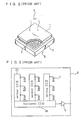
- a two-dimensional imaging array is shown in a perspective view in Figure 8.
- the array includes a two-dimensional array of photodiodes 1, for example, 128 x 128 photodiodes, for generating electrical signals in response to light incident on the respective photodiodes.
- the electrical signals generated comprise an electrical representation of the distribution of the incident light over a two-dimen sional area. That distribution of light, to the extent it is radiated by a source, is referred to here as the image.
- the photodiode array is mounted on and electrically connected to a silicon substrate 2 containing signal processing circuitry.
- Each photodiode is in electrical communication with a respective signal processing circuit in the substrate 2 through a columnar body 3, such as a cylindrical volume of indium.
- a columnar body 3 such as a cylindrical volume of indium.
- This construction is particularly applicable to an infrared light detector in which incident infrared rays 4 strike the photodiode array 1.
- the photodiodes may be made of a semiconductor material, such as cadmium mercury telluride (Cd x Hg 1-x Te), that, unlike silicon, responds to infrared light by generating electrical charges.
- An infrared-sensitive array like that of Figure 8 is described in U. S. Patent 4,801,991.
- the photodiode array 1, the silicon substrate 2 containing signal processing circuitry, and the columnar connectors 3 comprise an imaging array 6.
- the general electrical arrangement of the imaging array 6 is shown schematically in Figure 9 for a 3 x 3 array of photodiodes.
- the signal processing circuitry in the substrate 2 includes a charge coupled device (CCD) including, in the embodiment of Figure 9, a horizontal CCD 2a to which three vertical CCDs 2b are connected.
- CCD charge coupled device
- the orientation of these CCDs is referred to here as horizontal and vertical because of the orientation of Figure 9 and other figures.
- no limitation is implied by describing the CCDs as horizontal and vertical.
- orientational terms are used only for convenience and refer to two groups of generally orthogonal CCDs in which a plurality of CCDs oriented along one di rection are interconnected to a single CCD that is generally orthogonal to the interconnected CCDs.
- each photodiode 1 supplies electrical charges to one of the vertical CCDs 2b through which those charges are transferred to the horizontal CCD 2a.
- the collected charges are further transferred by the horizontal CCD 2a to an external device through an output circuit element 5, indicated as an amplifier in the figures.
- the imaging array 6 is interconnected with other components in an imaging apparatus.
- the imaging array provides electrical imaging signals, each signal representing the intensity of incident light at one of the locations of a photodiode array in a prearranged sequence related to photodiode locations, to a scan converter 7.
- the scan converter 7 uses the sequential electrical imaging signals to reconstruct a two-dimensional image which is displayed on a television monitor 8.
- a timing generator 9 provides timing signals to both the array 6 and the scan converter 7.
- incident light causes the photodiodes 1 to produce electrical charges that are conducted through the connectors 3 to the respective signal processing circuits in the substrate 2.
- That signal processing circuit stores the electrical charges and eventually transfers them in a timed sequence through the vertical CCDs 2b to the horizontal CCD 2a.
- the horizontal CCD 2a further transfers the stored electrical charges in a timed sequence through the output circuit 5 to the scan converter 7.
- the signals are prepared by the scan converter 7 to meet the specifications, e.g., length and number of lines, scanning rate, and so on, of the monitor 8 and are subsequently displayed on the monitor as an image.
- the structure of the array 6 shown in Figure 8 is particularly useful in an infrared detector where the photodiode array is made of a different material from the silicon substrate 2.
- the photodiodes may employ Cd 0.2 Hg 0.8 Te.
- the most difficult problem in detecting 10 micron band infrared images is the presence of significant amounts of background radiation.
- the background radiation is essentially noise that reduces image contrast.
- the technique commonly employed in other photodetectors to improve signal contrast, i.e., lengthening the time during which the signal charges are collected, is not successful in a photodetector responding to the 10 micron infrared band. Longer charge collection times only increase the quantity of charges generated by the background radiation, resulting in no signal-to-noise improvements.
- FIG. 11(a)-11(c) schematically illustrate signal processing circuitry of the type incorporated in the substrate 2 and employing the charge skimming method.
- an additional skimming terminal 19 also designated V sk , is connected to the signal processing circuitry as schematically shown in Figure 7.
- the circuitry of Figure 7 is analogous to that of Figure 9 but includes an additional connection from each of the signal processing circuits associated with the respective photodiodes 1 to the terminal 19.
- the photodiode 1 generates electrical charge in response to incident light 4. That charge flows into the signal processing circuitry at a contact 20 in the substrate 2.
- the inflowing charge creates a mirror charge region, i.e., the signal charge, in the substrate 2 indicated by the hatched area opposite the contact 20 in Figure 11(a).
- Those signal charges are further transferred from opposite the contact 20 to a potential well where they are stored.
- Charge transfer to the storage well is controlled by the magnitude of the voltage that is applied to a gate electrode 10.
- the storage well is created opposite a storage electrode 11 in response to a voltage applied to that electrode.
- a portion of the charge stored in the storage well is transferred to another potential well created opposite a CCD electrode 13.
- the transfer takes place upon the lowering of the potential barrier between the storage and CCD wells. That barrier is lowered by the application of a skimming voltage to the skimming electrode 12.
- a skimming voltage to the skimming electrode 12.
- FIG. 10(b) depending upon the magnitude of the skimming voltage, only an uppermost portion of the charge stored in the storage well has sufficient energy to flow over the lowered barrier and into the CCD well.
- the stored charge is "skimmed" in response to the voltage applied to the skimming electrode 12.
- the broken line 18 indicates a charge skimming level such that charges be low line 18 are discarded through the drain terminal 14 of Figure 11(c).
- the charges above line 18 are retained to produce the charge quantity as a function of array element shown in Figure 6(b).
- Comparison of Figures 6(a) and 6(b) shows that the desired image charges after skimming represent a much larger proportion of the total charge than without the application of the skimming technique. In other words, skimming improves the signal-to-noise ratio.
- some semiconductor materials such as Cd x Hg 1-x Te used in photodiodes sensitive to infrared light, have characteristics that are notoriously difficult to control, making the achievement of uniform sensitivities among many photodiodes virtually impossible.
- the photosensitivities of the photoresponsive elements vary significantly within the array, the advantages of the conventional charge skimming technique with conventional sensors are partially or totally lost.
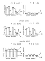
- FIG. 5(a) An example of significant variations in photodiode response within an array is illustrated in Figure 5(a).
- the area 16 corresponding to the background charges varies significantly amongst array elements.
- the skimming level 18 has to be less than the background response of the least sensitive element in the array.
- the skimmed charges illustrated in Figure 5(b) provide little improvement in discarding the background radiation compared to the response of Figure 5(a).
- a proposed solution, teaching away from the prior art and according to one aspect of the present invention, for applying the charge skimming technique to a photoresponsive array in which the light sensors have widely varying sensitivities is the application of different skimming levels to the respective signal processing circuits.
- the skimming levels are chosen to compensate for the sensitivities of the associated photodiodes.
- Application of different skimming levels to different array elements is illustrated in Figures 4(a) and 4(b).
- Figure 4(a) the background charge quantity 16 produced by each array element and the corresponding signal charge 17 produced by each element is illustrated as in Figures 5(a) and 6(a).
- skimming level 101 that may be different for each array element is applied to the respective photodiodes.
- the resulting skimmed signal is illustrated in Figure 4(b).
- the desired improvement in signal-to-noise ratio, i.e., contrast, achieved in Figure 6(b) is also achieved in Figure 4(b).
- An imaging array for applying variable magnitude skimming levels directly to respective signal processing circuitry could include a separate skimming electrode terminal for each of the signal processing circuits.
- a 128 x 128 photodiode array that arrangement would require more than 16,000 terminals.
- An imaging array with such a large number of terminals is extremely difficult, if not impossible, to realize practically, particularly in arrays including enough photodiodes to provide a useful image.
- a solid state imaging array includes a plurality of photoresponsive sensors for producing electrical charges in response to incident light, a signal processing circuit including a charge skimming electrode associated with each sensor for receiving and storing electrical charges from the associated sensor and for transferring to a respective charge coupled device a skimmed portion of the stored electrical charges, the skimmed portion being determined by the magnitude of a skimming voltage applied to the respective skimming electrode, a plurality of first charge coupled devices for receiving the skimmed portion of the electrical charges from the signal processing circuit and for transferring the skimmed portion to external circuitry, and means for applying different magnitude skimming voltages to each of the skimming electrodes, thereby compensating for variations in the photosensitivities of the individual sensor.
- the means for applying different skimming voltages includes a switching means associated with each of the signal processing circuits for converting skimming signals into skimming voltage magnitudes and for controlling the application of skimming voltage magnitudes to the respective skimming electrodes and a plurality of second charge coupled devices for simultaneously supplying the skimming signals to the respective switching means.
- a solid state imaging apparatus includes, in combination with the array, a memory for storing skimming levels corresponding to the magnitudes of the skimming voltages to be applied to the skimming electrodes and means for converting the stored skimming levels into skimming voltage magnitudes for applying those skimming voltages to the respective skimming electrodes.
- a preferred embodiment in which the skimming levels are stored in digital form includes a digital-to-analog converter for converting the stored levels into skimming signals for application to the respective signal processing circuits.
- the apparatus may include an analog-to-digital converter for receiving electrical charges transferred from the charge coupled devices while a uniform voltage is applied to the skimming electrodes under con trolled illumination and for converting the quantities of charges received into digital values, establishing the skimming levels for storage in the memory.
- An array of photosensors for forming an image is calibrated, according to the invention, by illuminating each of the photoresponsive sensors in the array with a controlled quantity of light, transferring the electrical charges produced by the respective sensors to produce correction signals establishing the relative photosensitivities of sensors for correcting the quantities of electrical charges produced by the respective sensors in response to light from an image and background light and thereby to compensate for variations in the photosensitivities of the individual sensors.
- the calibration method is applied to a solid state imaging array having a structure according to one aspect of the invention by applying a uniform magnitude voltage to each of the skimming electrodes in the array and transferring the electrical charges produced by the signal processing circuits for establishing the skimming levels required to compensate for the respective photosensitivities of the sensors.
- the controlled light may be of uniform intensity over the array or may vary in intensity over the array in correspondence with the background illumination incident on the array when no light from a desired image is present.
- a desired image is formed by calibrating an array of photosensors for forming an image, generating electrical charges in response to the incident light from the image and background, and correcting the electrical charges generated by the respective sensors with the correction signals produced in the calibration step.
- the desired image is formed, after calibrating the array, by applying the respective magnitudes of skimming voltages to the corresponding skimming electrodes and transferring the skimmed electrical charges to charge coupled devices for producing electrical imaging signals.
- the imaging signals may be employed with a scan converter for displaying a two-dimensional image corresponding to the image from which incident light falls on the array.
- FIG. 1 schematically shows a solid state imaging array 106 according to an embodiment of the present invention.
- Photoresponsive sensors in the form of photodiodes 1 are present for converting incident light into electrical charges. These photoresponsive sensors may respond to any portion of the visible or invisible light spectrum, but in one preferred application they are Cd 0.2 Hg 0.8 Te sensors responsive to infrared light of about 10 microns in wavelength.
- the sensors 1 are arranged in an array corresponding to respective picture elements or pixels of a two-dimensional image.
- Figure 1 shows a 3 x 3 array, i.e., an array including three sensors in each of three rows.
- the invention is not limited to a particular size array and, for example, may be employed with a 128 x 128 array or with arrays containing a still larger number of sensors. It is not necessary that the array be square, i.e., contain the same number of sensors in each column as appear in each row, or even rectangular and may have other shapes. It is assumed, however, that the array includes a plurality of rows and columns.
- Each of the sensors 1 in Figure 1 supplies electrical charges generated in response to incident light through a respective signal processing circuit to one of the vertical CCDs 2b.
- the signal processing circuitry is of the type described with respect to Figures 11(a) to 11(c).
- the charges that pass through the signal processing circuitry are transferred by the vertical CCDs 2b to a horizontal CCD 2a that is commonly connected to all of the vertical CCDs 2b.
- the transferred signals are collected in the horizontal CCD 2a and further transferred to an external device through the output circuit 5.
- Each of the vertical CCDs includes, for each respective sensor 1, a charge skimming electrode 12 to which a voltage is applied to determine the portion of the collected charge that is skimmed and further transferred to the respective vertical CCD 2b.
- the portion transferred depends on the magnitude of the skimming voltage as described above in relation to Figures 4(a) to 6(b) and 11(a) to 11(c).
- each of the skimming electrodes 12 in Figure 1 is not directly connected to an external terminal 19. Rather, a second CCD 102 including a single horizontal portion and a separate vertical portion for each of the corresponding vertical CCDs 2b is included.
- the second CCD 102 supplies, through an external terminal 103, skimming signals for applying skimming voltages of magnitudes chosen to compensate for variations in the photoresponse of the respective sensors 1 to the respective skimming electrodes.
- the CCDs 102 are connected to the respective skimming electrodes 12 when an appropriate gating voltage is applied to a terminal 104. That terminal 104 is electrically connected to each of the gates of a plurality of switching means 105.
- the gating voltage is applied through terminal 104 to actuate the switching means 105 and to connect the respective skimming signal, as a particular magnitude voltage, to the signal processing circuit for a respective sensor 1.
- the switching means 105 may include field effect transistors that are gated by a gating voltage applied to the terminal 104 in coordination with the application of the skimming signals sequentially to the terminal 103 of the array 106.
- FIG. 2(a) and 2(b) Particular structures of CCD 102 and of switching means 105 for receiving the skimming signals and for applying the skimming voltages to the skimming electrodes are shown in Figures 2(a) and 2(b).
- Figure 2(a) is a sectional view of a conventional four phase CCD. That CCD construction is one example of an embodiment of a vertical portion of the CCD 102 taken along line IIa-IIa of Figure 1.
- An insulator 202 such as silicon dioxide, which is disposed on substrate 201, such as silicon, forms, with the electrodes and interconnections 203, the four phase CCD.
- the CCD 102 is shown schematically as a continuous metallization in Figure 1, as understood in the art it includes a plurality of mutually insulated electrodes that are connected in sequence according to the number of phases of the CCD.
- charge carriers usually electrons
- This sequential transfer steps appropriate voltages along the CCD from the input terminal 103 to a position opposite a desired electrode of the CCD.
- Figure 2(b) is a highly schematic, complex sectional view of a preferred embodiment of a switching means 105 for applying a particular magnitude of skimming voltage to a respective signal processing circuit when the desired skimming signal appears at the desired location along the CCD 102. That desired location, for this example, is indicated in the upper half of Figure 2(b) by the electrode 203 which is the fourth phase of the four phase CCD. That electrode 203 is one of the electrodes appearing in the left-most vertical portion of CCD 102 in Figure 1.
- a gating signal is applied to the terminal 104. That gating signal actuates the switching means 105 by closing a switch, i.e., by lowering the potential barrier opposite electrode 104 of Figure 2(b). The lowered barrier transfers the skimming signal from electrode 203 to a skimming voltage output circuit 205.
- the circuit 205 includes a conventional floating diffusion amplifier having an electrically floating diffusion region 206. That amplifier resembles a gateless FET in which the region 206 is the source. The corresponding drain region is connected to a terminal 204 of a power supply V DD . The floating diffusion region 206 is electrically connected to the gate of an FET 207, such as a MOSFET. The source of transistor 207 is grounded and the drain is connected to the skimming electrode 12 as well as to the power supply terminal 204 through a load resistor.
- each switching means 105 in a preferred embodiment, includes two elements, i.e., the floating diffusion amplifier and the MOSFET, that are commonly formed on and in substrate 201. In order to show both of those elements, two separated sectional view portion are shown in Figure 2(b), although Figure 1 indicates that Figure 2(b) is taken only along a single section line.
- a signal containing all of the desired skimming signals in sequence is applied to terminal 103 and transferred along CCD 102 until the appropriate alignment of the respective skimming signals and the signal processing circuits is achieved.
- the gating signal is applied to the terminal 104 and the skimmed electrical imaging signal from each of the sensors 1 is transferred to the respective vertical CCD 2b for subsequent sequential transfer to horizontal CCD 2a and, through output circuit 5, to external circuitry.
- the desired application of individual skimming voltage magnitudes to the respective skimming electrodes 12 to compensate for differences in the photosensitivities of the respective sensors 1 is achieved through only two external terminals, namely, the skimming terminal 103 and the gating terminal 104. Therefore, individual terminals electrically connected to each of the skimming electrodes are unnecessary.
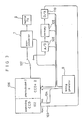
- Figure 3 shows an imaging apparatus including the imaging array 106 that has been described above.
- the apparatus includes the scan converter 7, the television monitor 8, and the timing generator 9 as described with reference to Figure 10.
- the timing generator 9 also supplies the gating signal to the gating terminal 104 of the array.
- the apparatus of Figure 3 includes a switch 107 for selectively sup plying the electrical imaging signals either to the scan converter 7 or to an analog-to-digital converter 108.
- the analog-to-digital converter 108 receives the analog signals from the array 106 when the switch 107 is connected to the converter 108 and provides digital signals to a memory 109.
- the memory 109 stores those digital signals and provides them to a digital-to-analog converter 110.
- the digital signals are converted back to analog form.
- the analog signals are the individual skimming signals for the array sensors 1.
- Those skimming signals are provided to the terminal 103 of the array 106 for transfer to the appropriate signal processing circuits through the CCD 102.
- the operations of the converters 108 and 110 and of the memory 109 must all be synchronized with other operations of the apparatus and, accordingly, each of them receives timing signals from the timing generator 9.
- the apparatus of Figure 3 is employed both for calibrating, i.e. establishing, the skimming voltage magnitudes for each of the skimming electrodes to compensate for variations in the sensitivities of the sensors and for operation, i.e., forming an image, from the electrical imaging signals.
- the light incident on the array is controlled.
- the array may be illuminated with light of uniform intensity or, preferably, any light from an image to be formed is prevented from reaching the array while the expected background light is permitted to reach the array. That background light may vary in intensity over the area of the array.
- the background light By using the background light to calibrate the array, variations in that background are incorporated into the skimming voltage magnitudes.
- the array 106 Upon achievement of the controlled illumination, the array 106 is operated normally with a uniform skimming voltage applied to each of the skimming electrodes 12.
- That uniform skimming voltage is chosen like the level 18 in Figure 5(a) so that some charge is generated even by the sensor producing the smallest quantity of charge, i.e., the least sensitive sensor.
- the switch 107 connected to the analog-to-digital converter 108, the electrical imaging signals produced by the array 106 are transmitted to the converter 108.
- the converter 108 changes the received signals from analog form to digital form and provides that digital output in a sequence corresponding to the geometric arrangement of the sensors according to the driving scheme employed with the CCDs 2a and 2b.
- Those digital signals are stored in the memory 109 as the skimming levels for subsequent use in generating skimming voltages.
- the uniform voltage applied to the skimming electrodes 12 may be zero. In that case, no signal is supplied to the CCD 102 through the terminal 103 and no gating signal is applied to the terminal 104. As a result, all the switching means 105 remain open so that no skimming voltage is applied to the individual skimming electrodes.
- the stored digital skimming levels are converted into analog skimming signals in the digital-to-analog converter 110.
- the digital skimming levels are supplied in sequence from the memory 109 under the control of the timing generator 9 to the converter 110.
- a sequential analog signal containing the skimming signals for each individual signal processing circuit is supplied from the converter 110 through the skimming voltage terminal 103 to the CCD 102.
- Those skimming signals are sequentially transferred along the CCD 102 until located adjacent the respective signal processing circuits.
- the timing generator 9 produces a gating signal, supplied through the terminal 104, actuating the switching means 105, producing and applying the respective magnitude skimming voltages to the respective skimming electrodes 12.
- the skimmed stored charges are then transferred to the vertical CCDs 2b as the electrical imaging signals, incorporating compensation for the photoresponse characteristics of the respective sensors 1.
- Those electrical imaging signals are provided through the switch 107 to the scan converter 7 and the monitor 8 where an image is formed and displayed in the manner already described with respect to Figure 10.
- the array of photosensors may employ other circuitry configurations for generating electrical imaging signals in response to the electrical charges produced by the photosensors. Even with different circuitry and structure, the aspect of the invention concerning the adjustment of the electrical imaging signals to compensate for variations in the photosensitivities of the individual photosensors can be applied.
- the array of photosensors for forming an image is first calibrated to determine the appropriate correction to compensate for variations in the photosensitivities of the photosensors.
- each of the sensors is illuminated with a controlled quantity of incident light in the absence of light from an image.
- the array of photosensors may be illuminated with light of the uniform intensity or with a varying intensity according to various compensation schemes. If the intensity distribution of the back ground light is known, it may be desirable to directly employ that background light in order to compensate not only for varying sensitivities of the photosensors but also variations in the background light intensity.
- each sensor In response to that light, each sensor generates electrical charges which are transferred to external circuitry to produce correction signals.
- the more sensitive photosensors produce relatively large quantities of electrical charges, resulting in a relatively large correction signal for adjusting the quantity of electrical charge produced by the photosensor in response to incident light from both an image and background light.
- an image is formed from the electrical charges produced by the sensors in response to incident light from an image and background light.
- the charges generated by the respective photosensors are corrected by applying the respective correction signals, for example, by subtracting the correction signal intensity from the signal produced by the generated electrical charges.
- the remaining electrical charges represent the image including compensation for the varying sensitivities of the photosensors.
- the corrections may be applied in the course of sequentially storing the imaging signals, in sequentially reading stored image signals from a memory, or otherwise. It is not essential, however, that the correction be made directly within the solid state imaging array.
Landscapes
- Engineering & Computer Science (AREA)
- Multimedia (AREA)
- Signal Processing (AREA)
- Transforming Light Signals Into Electric Signals (AREA)
- Solid State Image Pick-Up Elements (AREA)
Applications Claiming Priority (2)
| Application Number | Priority Date | Filing Date | Title |
|---|---|---|---|
| JP63305280A JPH0748826B2 (ja) | 1988-12-01 | 1988-12-01 | 固体撮像装置 |
| JP305280/88 | 1988-12-01 |
Publications (3)
| Publication Number | Publication Date |
|---|---|
| EP0371685A2 true EP0371685A2 (de) | 1990-06-06 |
| EP0371685A3 EP0371685A3 (en) | 1990-12-19 |
| EP0371685B1 EP0371685B1 (de) | 1996-03-13 |
Family
ID=17943200
Family Applications (1)
| Application Number | Title | Priority Date | Filing Date |
|---|---|---|---|
| EP89312119A Expired - Lifetime EP0371685B1 (de) | 1988-12-01 | 1989-11-22 | Festkörperbildmatrix, Vorrichtung und Bildherstellungsverfahren |
Country Status (4)
| Country | Link |
|---|---|
| US (1) | US5003565A (de) |
| EP (1) | EP0371685B1 (de) |
| JP (1) | JPH0748826B2 (de) |
| DE (1) | DE68925946T2 (de) |
Cited By (3)
| Publication number | Priority date | Publication date | Assignee | Title |
|---|---|---|---|---|
| FR2668873A1 (fr) * | 1990-11-05 | 1992-05-07 | Mitsubishi Electric Corp | Dispositif imageur a semiconducteurs et procede de commande de ce dispositif. |
| EP0793378A3 (de) * | 1996-02-27 | 1998-07-01 | Canon Kabushiki Kaisha | Photoelektrische Umwandlervorrichtung mit Ladungsabschöpfung |
| EP0853427A3 (de) * | 1994-06-01 | 1999-02-10 | Simage Oy | Vorrichtungen, Systeme und Methoden zur Aufnahme von Bildern |
Families Citing this family (12)
| Publication number | Priority date | Publication date | Assignee | Title |
|---|---|---|---|---|
| US5268583A (en) * | 1989-05-16 | 1993-12-07 | Sofradir - Societe Francaise De Detecteurs Infrarouges | Homogenizing electrical signals generated by a detection system and transmitted to an exploiting system |
| CA2095739A1 (en) * | 1992-05-27 | 1993-11-28 | Michael J. Mcnutt | Charge skimming and variable integration time in focal plane arrays |
| JP2551382B2 (ja) * | 1994-06-14 | 1996-11-06 | 日本電気株式会社 | 固体撮像装置 |
| JP3525500B2 (ja) * | 1994-07-26 | 2004-05-10 | ミノルタ株式会社 | 固体撮像装置 |
| US6087686A (en) * | 1997-12-29 | 2000-07-11 | Dalsa, Inc. | Pixel with buried channel spill well and transfer gate |
| US6504141B1 (en) * | 2000-09-29 | 2003-01-07 | Rockwell Science Center, Llc | Adaptive amplifier circuit with enhanced dynamic range |
| US7634376B2 (en) * | 2003-06-16 | 2009-12-15 | Aptina Imaging Corporation | Internal bias measure with onboard ADC for electronic devices |
| KR100969905B1 (ko) * | 2005-11-14 | 2010-07-13 | 파나소닉 전공 주식회사 | 공간 정보 검출 장치 및 이에 적합한 광검출 소자 |
| JP5171158B2 (ja) * | 2007-08-22 | 2013-03-27 | 浜松ホトニクス株式会社 | 固体撮像装置及び距離画像測定装置 |
| JP2009130015A (ja) * | 2007-11-21 | 2009-06-11 | Sanyo Electric Co Ltd | 撮像装置 |
| JP5356726B2 (ja) * | 2008-05-15 | 2013-12-04 | 浜松ホトニクス株式会社 | 距離センサ及び距離画像センサ |
| US8605181B2 (en) | 2010-11-29 | 2013-12-10 | Teledyne Dalsa B.V. | Pixel for correlated double sampling with global shutter |
Family Cites Families (11)
| Publication number | Priority date | Publication date | Assignee | Title |
|---|---|---|---|---|
| GB1437328A (en) * | 1972-09-25 | 1976-05-26 | Rca Corp | Sensors having recycling means |
| US3845295A (en) * | 1973-05-02 | 1974-10-29 | Rca Corp | Charge-coupled radiation sensing circuit with charge skim-off and reset |
| US3969634A (en) * | 1975-07-31 | 1976-07-13 | Hughes Aircraft Company | Bucket background subtraction circuit for charge-coupled devices |
| US4197553A (en) * | 1976-09-07 | 1980-04-08 | Hughes Aircraft Company | Monolithic extrinsic silicon infrared detector structure employing multi-epitaxial layers |
| US4213137A (en) * | 1976-11-16 | 1980-07-15 | Hughes Aircraft Company | Monolithic variable size detector |
| US4585934A (en) * | 1979-03-05 | 1986-04-29 | Hughes Aircraft Company | Self-calibration technique for charge-coupled device imagers |
| FR2548498B1 (fr) * | 1983-06-28 | 1985-10-18 | Thomson Csf | Procede de correction du niveau en sortie d'un dispositif a transfert de charge et dispositif pour sa mise en oeuvre |
| US4620231A (en) * | 1984-06-18 | 1986-10-28 | Rca Corporation | CCD imager with photodetector bias introduced via the CCD register |
| DE3625010C2 (de) * | 1986-07-24 | 1995-01-19 | Telefunken Microelectron | Verfahren zur Übergabe von hintergrundsignalbefreiten Nutzsignalen |
| FR2608315B1 (fr) * | 1986-12-16 | 1989-02-17 | Thomson Csf | Dispositif anti-eblouissement pour capteur d'images a transfert de charges et capteur d'images comportant un tel dispositif |
| JPH069240B2 (ja) * | 1987-07-17 | 1994-02-02 | 三菱電機株式会社 | 半導体受光装置 |
-
1988
- 1988-12-01 JP JP63305280A patent/JPH0748826B2/ja not_active Expired - Lifetime
-
1989
- 1989-11-21 US US07/439,325 patent/US5003565A/en not_active Expired - Fee Related
- 1989-11-22 DE DE68925946T patent/DE68925946T2/de not_active Expired - Fee Related
- 1989-11-22 EP EP89312119A patent/EP0371685B1/de not_active Expired - Lifetime
Cited By (4)
| Publication number | Priority date | Publication date | Assignee | Title |
|---|---|---|---|---|
| FR2668873A1 (fr) * | 1990-11-05 | 1992-05-07 | Mitsubishi Electric Corp | Dispositif imageur a semiconducteurs et procede de commande de ce dispositif. |
| GB2249430B (en) * | 1990-11-05 | 1995-01-18 | Mitsubishi Electric Corp | A solid-state imaging device |
| EP0853427A3 (de) * | 1994-06-01 | 1999-02-10 | Simage Oy | Vorrichtungen, Systeme und Methoden zur Aufnahme von Bildern |
| EP0793378A3 (de) * | 1996-02-27 | 1998-07-01 | Canon Kabushiki Kaisha | Photoelektrische Umwandlervorrichtung mit Ladungsabschöpfung |
Also Published As
| Publication number | Publication date |
|---|---|
| DE68925946T2 (de) | 1996-08-08 |
| EP0371685B1 (de) | 1996-03-13 |
| JPH02151183A (ja) | 1990-06-11 |
| JPH0748826B2 (ja) | 1995-05-24 |
| EP0371685A3 (en) | 1990-12-19 |
| DE68925946D1 (de) | 1996-04-18 |
| US5003565A (en) | 1991-03-26 |
Similar Documents
| Publication | Publication Date | Title |
|---|---|---|
| EP0371685A2 (de) | Festkörperbildmatrix, Vorrichtung und Bildherstellungsverfahren | |
| US4407010A (en) | Solid state image pickup device | |
| US4835404A (en) | Photoelectric converting apparatus with a switching circuit and a resetting circuit for reading and resetting a plurality of lines sensors | |
| US5463420A (en) | Photoelectric conversion system | |
| US5436476A (en) | CCD image sensor with active transistor pixel | |
| TWI475884B (zh) | 數位放射線照相成像裝置 | |
| US4169273A (en) | Photodetector signal processing | |
| US4980546A (en) | Photosensitive device of the type with amplification of the signal at the photosensitive dots | |
| US5146302A (en) | Charge skimming solid-state imaging device including sampling circuits | |
| CA1169529A (en) | Solid state imaging apparatus | |
| US4891682A (en) | Solid state image pick-up device having a number of static induction transistor image sensors | |
| EP0655860B1 (de) | Bildaufnahmevorrichtung | |
| KR100265269B1 (ko) | 수직 오버플로우 드레인 및 저항성 게이트 전하 전송소자를 가지는 고체촬상소자 및 그 제어방법 | |
| US4868405A (en) | Photoelectric converting apparatus having a common region connecting either sources or drains to a common signal line | |
| EP0061491B1 (de) | Automatische ansprechempfindlichkeitsregelung für eine ccd-abbildungsvorrichtung | |
| EP0479534B1 (de) | Fotovoltaischer Wandler | |
| US4833515A (en) | Imaging devices comprising photovoltaic detector elements | |
| EP0131048B1 (de) | Mit ladungskopplung arbeitende bildsensorschaltung mit schwachem rauschen | |
| US5168338A (en) | Solid-state hybrid infrared imaging device | |
| US4808834A (en) | Solid-state image sensor | |
| WO1991006124A1 (en) | Solid-state image sensor | |
| EP0215531B1 (de) | Bildaufnahmeanordnungen mit photovoltaischen Detektorelementen | |
| US7054041B2 (en) | Image sensor method and apparatus having addressable pixels and non-destructive readout | |
| US4266237A (en) | Semiconductor apparatus | |
| GB2270228A (en) | Infrared imaging array - speeding charge transfer. |
Legal Events
| Date | Code | Title | Description |
|---|---|---|---|
| PUAI | Public reference made under article 153(3) epc to a published international application that has entered the european phase |
Free format text: ORIGINAL CODE: 0009012 |
|
| AK | Designated contracting states |
Kind code of ref document: A2 Designated state(s): DE FR GB |
|
| PUAL | Search report despatched |
Free format text: ORIGINAL CODE: 0009013 |
|
| AK | Designated contracting states |
Kind code of ref document: A3 Designated state(s): DE FR GB |
|
| RHK1 | Main classification (correction) |
Ipc: H01L 27/148 |
|
| 17P | Request for examination filed |
Effective date: 19901228 |
|
| 17Q | First examination report despatched |
Effective date: 19931116 |
|
| GRAA | (expected) grant |
Free format text: ORIGINAL CODE: 0009210 |
|
| AK | Designated contracting states |
Kind code of ref document: B1 Designated state(s): DE FR GB |
|
| REF | Corresponds to: |
Ref document number: 68925946 Country of ref document: DE Date of ref document: 19960418 |
|
| ET | Fr: translation filed | ||
| PLBE | No opposition filed within time limit |
Free format text: ORIGINAL CODE: 0009261 |
|
| STAA | Information on the status of an ep patent application or granted ep patent |
Free format text: STATUS: NO OPPOSITION FILED WITHIN TIME LIMIT |
|
| 26N | No opposition filed | ||
| PGFP | Annual fee paid to national office [announced via postgrant information from national office to epo] |
Ref country code: FR Payment date: 19981110 Year of fee payment: 10 |
|
| PGFP | Annual fee paid to national office [announced via postgrant information from national office to epo] |
Ref country code: GB Payment date: 19981127 Year of fee payment: 10 |
|
| PGFP | Annual fee paid to national office [announced via postgrant information from national office to epo] |
Ref country code: DE Payment date: 19981130 Year of fee payment: 10 |
|
| PG25 | Lapsed in a contracting state [announced via postgrant information from national office to epo] |
Ref country code: GB Free format text: LAPSE BECAUSE OF NON-PAYMENT OF DUE FEES Effective date: 19991122 |
|
| GBPC | Gb: european patent ceased through non-payment of renewal fee |
Effective date: 19991122 |
|
| PG25 | Lapsed in a contracting state [announced via postgrant information from national office to epo] |
Ref country code: FR Free format text: LAPSE BECAUSE OF NON-PAYMENT OF DUE FEES Effective date: 20000731 |
|
| PG25 | Lapsed in a contracting state [announced via postgrant information from national office to epo] |
Ref country code: DE Free format text: LAPSE BECAUSE OF NON-PAYMENT OF DUE FEES Effective date: 20000901 |
|
| REG | Reference to a national code |
Ref country code: FR Ref legal event code: ST |