EP0371901A2 - Dicke epitaktische Filme mit abrupten Übergängen - Google Patents
Dicke epitaktische Filme mit abrupten Übergängen Download PDFInfo
- Publication number
- EP0371901A2 EP0371901A2 EP89480150A EP89480150A EP0371901A2 EP 0371901 A2 EP0371901 A2 EP 0371901A2 EP 89480150 A EP89480150 A EP 89480150A EP 89480150 A EP89480150 A EP 89480150A EP 0371901 A2 EP0371901 A2 EP 0371901A2
- Authority
- EP
- European Patent Office
- Prior art keywords
- layer
- deposition
- epitaxial
- less
- epitaxial film
- Prior art date
- Legal status (The legal status is an assumption and is not a legal conclusion. Google has not performed a legal analysis and makes no representation as to the accuracy of the status listed.)
- Withdrawn
Links
Images


Classifications
-
- H—ELECTRICITY
- H10—SEMICONDUCTOR DEVICES; ELECTRIC SOLID-STATE DEVICES NOT OTHERWISE PROVIDED FOR
- H10P—GENERIC PROCESSES OR APPARATUS FOR THE MANUFACTURE OR TREATMENT OF DEVICES COVERED BY CLASS H10
- H10P14/00—Formation of materials, e.g. in the shape of layers or pillars
- H10P14/20—Formation of materials, e.g. in the shape of layers or pillars of semiconductor materials
- H10P14/24—Formation of materials, e.g. in the shape of layers or pillars of semiconductor materials using chemical vapour deposition [CVD]
-
- H—ELECTRICITY
- H10—SEMICONDUCTOR DEVICES; ELECTRIC SOLID-STATE DEVICES NOT OTHERWISE PROVIDED FOR
- H10P—GENERIC PROCESSES OR APPARATUS FOR THE MANUFACTURE OR TREATMENT OF DEVICES COVERED BY CLASS H10
- H10P14/00—Formation of materials, e.g. in the shape of layers or pillars
- H10P14/20—Formation of materials, e.g. in the shape of layers or pillars of semiconductor materials
- H10P14/29—Formation of materials, e.g. in the shape of layers or pillars of semiconductor materials characterised by the substrates
- H10P14/2901—Materials
- H10P14/2902—Materials being Group IVA materials
- H10P14/2905—Silicon, silicon germanium or germanium
-
- H—ELECTRICITY
- H10—SEMICONDUCTOR DEVICES; ELECTRIC SOLID-STATE DEVICES NOT OTHERWISE PROVIDED FOR
- H10P—GENERIC PROCESSES OR APPARATUS FOR THE MANUFACTURE OR TREATMENT OF DEVICES COVERED BY CLASS H10
- H10P14/00—Formation of materials, e.g. in the shape of layers or pillars
- H10P14/20—Formation of materials, e.g. in the shape of layers or pillars of semiconductor materials
- H10P14/32—Formation of materials, e.g. in the shape of layers or pillars of semiconductor materials characterised by intermediate layers between substrates and deposited layers
- H10P14/3202—Materials thereof
- H10P14/3204—Materials thereof being Group IVA semiconducting materials
- H10P14/3211—Silicon, silicon germanium or germanium
-
- H—ELECTRICITY
- H10—SEMICONDUCTOR DEVICES; ELECTRIC SOLID-STATE DEVICES NOT OTHERWISE PROVIDED FOR
- H10P—GENERIC PROCESSES OR APPARATUS FOR THE MANUFACTURE OR TREATMENT OF DEVICES COVERED BY CLASS H10
- H10P14/00—Formation of materials, e.g. in the shape of layers or pillars
- H10P14/20—Formation of materials, e.g. in the shape of layers or pillars of semiconductor materials
- H10P14/34—Deposited materials, e.g. layers
- H10P14/3402—Deposited materials, e.g. layers characterised by the chemical composition
- H10P14/3404—Deposited materials, e.g. layers characterised by the chemical composition being Group IVA materials
- H10P14/3411—Silicon, silicon germanium or germanium
-
- H—ELECTRICITY
- H10—SEMICONDUCTOR DEVICES; ELECTRIC SOLID-STATE DEVICES NOT OTHERWISE PROVIDED FOR
- H10P—GENERIC PROCESSES OR APPARATUS FOR THE MANUFACTURE OR TREATMENT OF DEVICES COVERED BY CLASS H10
- H10P32/00—Diffusion of dopants within, into or out of wafers, substrates or parts of devices
- H10P32/10—Diffusion of dopants within, into or out of semiconductor bodies or layers
- H10P32/15—Diffusion of dopants within, into or out of semiconductor bodies or layers from the substrate during epitaxy, e.g. autodoping; Preventing or using autodoping
Definitions
- This invention relates to the deposition of epitaxial silicon layers in semiconductor devices and more particularly to a method for growing epitaxial silicon films with minimal autodoping using low temperature epitaxial film growth followed by a higher temperature epitaxial film growth.
- One such parameter is the thickness of the epitaxial film deposited on doped substrates. Because of autodoping problems of the epitaxial layer caused by vapor out-gassing of impurities from the substrate into said layer, the dimensions of these layers deposited by silicon epitaxy have been limited to magnitudes greater than the thickness required to overcome the out-gassed dopants. This length is about 1 micron under conventional (T is greater than 1000°C) processing conditions. The incorporation of these out-gassed dopants has similarly prevented the formation of abrupt dopant transition widths.
- CVD chemical vapor deposition
- an object of the present invention to provide a method for epitaxial depositions on silicon wafers wherein out diffusion, and/or autodoping from the wafer can be contained to minimum diffusion lengths.
- said second layer of epitaxial growth is deposited by conventional techniques at temperatures greater than 800°C.
- the thickness of said second layer being greater than or equal to the thickness of said first layer.
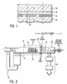
- Figure 1 is a cross-section view of an N- doped semiconductor substrate 30 containing two embedded doped regions 32 and 34 which are P+ and N+ respectively.
- substrate 1 is a monocrystalline silicon structure of conventional thickness and doped N- type to a resistivity of at least about 0.1 ohm-cm.
- Embedded in substrate 30 by conventional techniques is an N+ type region 34 and a Pregion 32.
- Forming the N+ region 34 may be accomplished in conjunction with well-known masking techniques by employing N-type impurities such as arsenic or phosphorous as the dopant to produce a high doping level which normally extends in the range of about 1 x 10²⁰ to about 1 x 10²¹ atoms per cubic centimeter to provide a relatively low resistivity in the range of about 8 x 10 ⁇ 4 to about 3 x 10 ⁇ 4 ohm-cm.
- region 34 is of the same conductivity type as substrate 30.
- the P+ region 32 defining the P/N junction may be formed, also in conjunction with masking techniques, by diffusion employing P- type impurities such as boron as the diffusant to produce a relatively high doping level which normally extends in the range of about 2 x 10²⁰ atoms per cubic centimeter to provide a corresponding low resistivity region in the range of about 7 x 10 ⁇ 4 ohms-cm.
- the P+ doped region 32 is of a conductivity type opposite to the conductivity of substrate 30.
- the substrate may be devoid of doped regions, and thus merely comprise a doped region of one conductivity type on which is to be deposited semiconductor material of a second conductivity type to define a P/N junction.
- either type of doped regions may be employed alone to the exclusion of the other type.
- the invention is also directed to deposition of doped semiconductor materials on a semiconductor substrate of the same conductivity type.
- a thin film (about 100 ⁇ ) of N doped silicon 36 is deposited by a low temperature epitaxial technique.
- a thin film (about 100 ⁇ ) of N doped silicon 36 is deposited by a low temperature epitaxial technique.
- high quality, low temperature epitaxial layers are recent techniques, the method and apparatus for deposition of this low temperature epitaxial layer is shown in detail in Figure 2.
- Figure 2 is a layout plan for one type of low-temperature, low-pressure; CVD epitaxy growth apparatus.
- a UHV section 10 (deposition chamber, or reactor) and a load chamber section 12 is used to load substrates 14 into the UHV section 10.
- a main valve 16 serves as an isolation between UHV section 10 and the load chamber 12.
- loading chamber 12 The function of loading chamber 12 is to provide a low-pressure chamber from which the substrates 14 are transferred into to UHV section 10 after the load chamber 12 has been pumped to a pressure below 10 ⁇ 6 Torr.
- Loading chamber 12 is comprised of pumping means 20 for evacuating the chamber 12 to the desired vacuum level. Also attached to load chamber 12 is transfer means 28 for transferring the substrates 14 from the load chamber into the UHV section.
- the UHV section (also termed a reactor, or deposition chamber) is generally comprised of a hot-wall furnace in which chemical vapor deposition onto the substrates occurs, and optionally instrumentation (mass spectrometer) for determining the impurity levels in the furnace, and pumping means for creating an ultimate vacuum at least 10 ⁇ 8 Torr in the furnace
- Pumping means 38 is used to establish an ultimate vacuum at least 10 ⁇ 8 Torr in the tube 34.
- the provision of a load chamber means 12 and means 38 to provide an ultrahigh vacuum in the deposition tube of a CVD apparatus is essential to the deposition of epitaxial silicon layers of high quality onto the substrates 14.
- the source gases and any dopant gases are injected into tube 34 via the gas source inlet 56.
- the operating deposition temperature is less than about 800°C, and the operating total pressure is generally less than about 200 mTorr. Further, the apparatus is operated such that the partial pressures of all contaminants in UHV section 10 are maintained less than 10 ⁇ 8 Torr at all times, that is, prior to deposition and during deposition onto the substrates 14.
- N-layer 38 onto the low-temperature epitaxial layer 36 is then deposited a N-layer 38.
- This layer 38 is not critical and any of a number of conventional methods can be used.
- Epitaxial deposition equipment for these processes have included both vertical and pancake reactors using source gases such as SiH4, SiH2Cl2, SiHCl3 and SiCl4 with H2.
- source gases such as SiH4, SiH2Cl2, SiHCl3 and SiCl4 with H2.
- Recent reviews describing processes suited for such deposition include (e.g. "Silicon Epitaxy,” Nov. 1978, SOLID STATE TECHNOLOGY, pp. 103-106, respectively).
- the substrate is heated in a vertical reactor and the deposition is carried out at an operating pressure of 35 Torr at a temperature of 860°C employing SiCl4 and H2 as reactants.
- Arsine was employed as the dopant and introduced as a controlled trace gas at 50 ppm. The gases were passed over the substrate at 40 lpm until the desired thickness was achieved, which for practical purposes can normally extend in the range of about 1 to 5 microns.
- the dopant will be omitted from the feed gas; and conversely if an N-type epitaxial layer is desired a corresponding type of conductivity deter-mining impurity, such as phosphine or arsine may be added to the feed gas.
- a corresponding type of conductivity deter-mining impurity such as phosphine or arsine may be added to the feed gas.
- various dopant concentrations can be employed depending upon the desired characteristics of the deposited epitaxial layer.
- FIG. 3A is the SIMS profile for this N-epitaxial growth 38 over the P+ implant 32 (without the intervening low temperature epitaxial film 36 as shown in Figure 1) along the same cross-sections as indicated by the broken line in Figure 1.
- Figure 3B is the SIMS profile for the N- epitaxial growth 38 over the N+ implant 34 (again without the intervening low temperature epitaxial film 36 as shown in Figure 1) along the cross-section as indicated by its respective broken line. Both above regions are on substrate 30.
- figures 4A and 4B show the SIMS curves for an embodiment of a medium temperature epitaxial layer deposited on a low-temperature layer on a similarly doped substrate.
- Figures 4A shows the epitaxial deposit of an N- doped layer on a P+ substrate region along the same line as discussed above.
- the medium temperature N- epitaxial layer 38 is about 1 x 10⁴ ⁇ deep.
- the autodoping of the arsenic in the immediate surface boundary between layers 36 and 32 can now be seen to be significantly less than the boron concentration at the same boundary in Figure 3A. From Figure 4A, it can be seen that at a surface depth of 1.25 x 10⁴ ⁇ that the boron concentration is 1019/cm3 while the arsenic concentration has been controlled to under 1017/cm3. This is an extensive improvement in controlling auto-doping over that shown in Figure 3A for growing medium temperature epitaxial layers.
- the depositions can now be performed within acceptable time limits.
- the low temperature processing time has been kept to a minimum as only a thin 400 ⁇ layer was deposited.
- the remaining thickness of epitaxial deposit was made up of the medium temperature growth which in comparison is about 20 times as fast as the low temperature growth.
- Conventional medium to high temperature depositions take place at about a rate of 1 micron/5 minutes as compared to 100 ⁇ /minute or 1 micron/100 minutes for low temperature deposits.
Applications Claiming Priority (2)
| Application Number | Priority Date | Filing Date | Title |
|---|---|---|---|
| US25937788A | 1988-10-18 | 1988-10-18 | |
| US259377 | 1988-10-18 |
Publications (2)
| Publication Number | Publication Date |
|---|---|
| EP0371901A2 true EP0371901A2 (de) | 1990-06-06 |
| EP0371901A3 EP0371901A3 (de) | 1990-06-13 |
Family
ID=22984691
Family Applications (1)
| Application Number | Title | Priority Date | Filing Date |
|---|---|---|---|
| EP89480150A Withdrawn EP0371901A3 (de) | 1988-10-18 | 1989-09-26 | Dicke epitaktische Filme mit abrupten Übergängen |
Country Status (2)
| Country | Link |
|---|---|
| EP (1) | EP0371901A3 (de) |
| JP (1) | JPH0714840B2 (de) |
Cited By (4)
| Publication number | Priority date | Publication date | Assignee | Title |
|---|---|---|---|---|
| EP0540443A3 (en) * | 1991-10-31 | 1996-09-25 | Ibm | Complementary subcollectors with silicon epitaxial layers |
| WO2001009942A1 (en) * | 1999-08-02 | 2001-02-08 | Shine S.P.A. | Process for forming structure with different doped regions, showing a hyperfine transition region, for forming porous silicon |
| CN116884832A (zh) * | 2023-09-06 | 2023-10-13 | 合肥晶合集成电路股份有限公司 | 半导体器件及其制作方法 |
| EP4576168A1 (de) * | 2023-12-22 | 2025-06-25 | Nexperia B.V. | Unterdrückung der selbstdotierung während des epitaktischen wachstums einer epitaxie-schicht in einer halbleitervorrichtung |
Families Citing this family (1)
| Publication number | Priority date | Publication date | Assignee | Title |
|---|---|---|---|---|
| JP5458190B2 (ja) * | 2013-01-22 | 2014-04-02 | Sumco Techxiv株式会社 | エピタキシャルウェーハの製造方法及びエピタキシャルウェーハ |
Family Cites Families (5)
| Publication number | Priority date | Publication date | Assignee | Title |
|---|---|---|---|---|
| FR2076117B1 (de) * | 1970-01-15 | 1973-11-23 | Ibm | |
| US3847686A (en) * | 1970-05-27 | 1974-11-12 | Gen Electric | Method of forming silicon epitaxial layers |
| US4579609A (en) * | 1984-06-08 | 1986-04-01 | Massachusetts Institute Of Technology | Growth of epitaxial films by chemical vapor deposition utilizing a surface cleaning step immediately before deposition |
| JPH01161826A (ja) * | 1987-12-18 | 1989-06-26 | Toshiba Corp | 気相エピタキシャル成長法 |
| JPH01179797A (ja) * | 1988-01-07 | 1989-07-17 | Nec Corp | 半導体結晶成長方法 |
-
1989
- 1989-08-11 JP JP1207101A patent/JPH0714840B2/ja not_active Expired - Lifetime
- 1989-09-26 EP EP89480150A patent/EP0371901A3/de not_active Withdrawn
Cited By (5)
| Publication number | Priority date | Publication date | Assignee | Title |
|---|---|---|---|---|
| EP0540443A3 (en) * | 1991-10-31 | 1996-09-25 | Ibm | Complementary subcollectors with silicon epitaxial layers |
| WO2001009942A1 (en) * | 1999-08-02 | 2001-02-08 | Shine S.P.A. | Process for forming structure with different doped regions, showing a hyperfine transition region, for forming porous silicon |
| CN116884832A (zh) * | 2023-09-06 | 2023-10-13 | 合肥晶合集成电路股份有限公司 | 半导体器件及其制作方法 |
| CN116884832B (zh) * | 2023-09-06 | 2023-12-15 | 合肥晶合集成电路股份有限公司 | 半导体器件及其制作方法 |
| EP4576168A1 (de) * | 2023-12-22 | 2025-06-25 | Nexperia B.V. | Unterdrückung der selbstdotierung während des epitaktischen wachstums einer epitaxie-schicht in einer halbleitervorrichtung |
Also Published As
| Publication number | Publication date |
|---|---|
| EP0371901A3 (de) | 1990-06-13 |
| JPH02116700A (ja) | 1990-05-01 |
| JPH0714840B2 (ja) | 1995-02-22 |
Similar Documents
| Publication | Publication Date | Title |
|---|---|---|
| CA1327935C (en) | Growth of beta-sic thin films and semiconductor devices fabricated thereon | |
| RU2764040C2 (ru) | ВЫРАЩИВАНИЕ ЭПИТАКСИАЛЬНОГО 3C-SiC НА МОНОКРИСТАЛЛИЧЕСКОМ КРЕМНИИ | |
| US5607511A (en) | Method and apparatus for low temperature, low pressure chemical vapor deposition of epitaxial silicon layers | |
| US5298452A (en) | Method and apparatus for low temperature, low pressure chemical vapor deposition of epitaxial silicon layers | |
| US5709745A (en) | Compound semi-conductors and controlled doping thereof | |
| KR100450316B1 (ko) | 탄화 규소 및 이의 제조 방법 | |
| US7402504B2 (en) | Epitaxial semiconductor deposition methods and structures | |
| US7682947B2 (en) | Epitaxial semiconductor deposition methods and structures | |
| EP0069580B1 (de) | Verfahren zur Herstellung von dünnen Schichten aus Silizium | |
| US5141893A (en) | Growth of P type Group III-V compound semiconductor on Group IV semiconductor substrate | |
| US3669769A (en) | Method for minimizing autodoping in epitaxial deposition | |
| US3765960A (en) | Method for minimizing autodoping in epitaxial deposition | |
| US8329532B2 (en) | Process for the simultaneous deposition of crystalline and amorphous layers with doping | |
| US7358112B2 (en) | Method of growing a semiconductor layer | |
| CA1328796C (en) | Method and apparatus for low temperature, low pressure chemical vapor deposition of epitaxial silicon layers | |
| EP1604395A2 (de) | Epitaxialhalbleiterablagerungsverfahren und -strukturen | |
| US5324685A (en) | Method for fabricating a multilayer epitaxial structure | |
| US5141569A (en) | Growth of P type Group III-V compound semiconductor on Group IV semiconductor substrate | |
| Ohshita | Low Temperature P‐Doped SiC Growth by Chemical Vapor Deposition Using CH 3SiH3/PH 3 Gas | |
| GB2395839A (en) | MBE growth of p-type nitride semiconductor materials | |
| JPH0714840B2 (ja) | エピタキシャル膜成長方法 | |
| US5306660A (en) | Technique for doping mercury cadmium telluride MOCVD grown crystalline materials using free radical transport of elemental indium and apparatus therefor | |
| Nagao et al. | Crystalline film quality in reduced pressure silicon epitaxy at low temperature | |
| Hoyt | Rapid thermal processing‐based epitaxy | |
| EP0490531A2 (de) | Si/Ge legierte Halbleitervorrichtungen |
Legal Events
| Date | Code | Title | Description |
|---|---|---|---|
| PUAI | Public reference made under article 153(3) epc to a published international application that has entered the european phase |
Free format text: ORIGINAL CODE: 0009012 |
|
| PUAL | Search report despatched |
Free format text: ORIGINAL CODE: 0009013 |
|
| AK | Designated contracting states |
Kind code of ref document: A2 Designated state(s): DE FR GB |
|
| AK | Designated contracting states |
Kind code of ref document: A3 Designated state(s): DE FR GB |
|
| 17P | Request for examination filed |
Effective date: 19900820 |
|
| 17Q | First examination report despatched |
Effective date: 19921111 |
|
| STAA | Information on the status of an ep patent application or granted ep patent |
Free format text: STATUS: THE APPLICATION IS DEEMED TO BE WITHDRAWN |
|
| 18D | Application deemed to be withdrawn |
Effective date: 19930323 |