EP0372072B1 - Plasma-schalter mit einer chrom-kathode mit strukturierter oberfläche - Google Patents
Plasma-schalter mit einer chrom-kathode mit strukturierter oberfläche Download PDFInfo
- Publication number
- EP0372072B1 EP0372072B1 EP89908112A EP89908112A EP0372072B1 EP 0372072 B1 EP0372072 B1 EP 0372072B1 EP 89908112 A EP89908112 A EP 89908112A EP 89908112 A EP89908112 A EP 89908112A EP 0372072 B1 EP0372072 B1 EP 0372072B1
- Authority
- EP
- European Patent Office
- Prior art keywords
- cathode
- plasma
- switch
- chromium
- perturbations
- Prior art date
- Legal status (The legal status is an assumption and is not a legal conclusion. Google has not performed a legal analysis and makes no representation as to the accuracy of the status listed.)
- Expired - Lifetime
Links
- VYZAMTAEIAYCRO-UHFFFAOYSA-N Chromium Chemical compound [Cr] VYZAMTAEIAYCRO-UHFFFAOYSA-N 0.000 title claims abstract description 40
- 229910052804 chromium Inorganic materials 0.000 claims abstract description 37
- 239000011651 chromium Substances 0.000 claims abstract description 37
- 239000000203 mixture Substances 0.000 claims abstract description 10
- 239000000463 material Substances 0.000 claims description 15
- ZOKXTWBITQBERF-UHFFFAOYSA-N Molybdenum Chemical compound [Mo] ZOKXTWBITQBERF-UHFFFAOYSA-N 0.000 claims description 11
- 229910052750 molybdenum Inorganic materials 0.000 claims description 9
- 239000011733 molybdenum Substances 0.000 claims description 9
- 239000002344 surface layer Substances 0.000 claims description 6
- WFKWXMTUELFFGS-UHFFFAOYSA-N tungsten Chemical compound [W] WFKWXMTUELFFGS-UHFFFAOYSA-N 0.000 claims description 5
- 229910052721 tungsten Inorganic materials 0.000 claims description 5
- 239000010937 tungsten Substances 0.000 claims description 5
- ZSLUVFAKFWKJRC-IGMARMGPSA-N 232Th Chemical compound [232Th] ZSLUVFAKFWKJRC-IGMARMGPSA-N 0.000 claims description 3
- 229910052776 Thorium Inorganic materials 0.000 claims description 3
- WGLPBDUCMAPZCE-UHFFFAOYSA-N Trioxochromium Chemical compound O=[Cr](=O)=O WGLPBDUCMAPZCE-UHFFFAOYSA-N 0.000 claims description 3
- 229910000423 chromium oxide Inorganic materials 0.000 claims description 3
- 238000000576 coating method Methods 0.000 abstract description 13
- 239000011248 coating agent Substances 0.000 abstract description 12
- 238000004544 sputter deposition Methods 0.000 abstract description 2
- 239000007789 gas Substances 0.000 description 10
- 150000002500 ions Chemical class 0.000 description 9
- 239000010410 layer Substances 0.000 description 8
- 229910052782 aluminium Inorganic materials 0.000 description 6
- XAGFODPZIPBFFR-UHFFFAOYSA-N aluminium Chemical compound [Al] XAGFODPZIPBFFR-UHFFFAOYSA-N 0.000 description 6
- 238000000034 method Methods 0.000 description 5
- RYGMFSIKBFXOCR-UHFFFAOYSA-N Copper Chemical compound [Cu] RYGMFSIKBFXOCR-UHFFFAOYSA-N 0.000 description 4
- 229910052802 copper Inorganic materials 0.000 description 4
- 239000010949 copper Substances 0.000 description 4
- 239000001257 hydrogen Substances 0.000 description 4
- 229910052739 hydrogen Inorganic materials 0.000 description 4
- 230000008569 process Effects 0.000 description 4
- 238000004519 manufacturing process Methods 0.000 description 3
- 230000007935 neutral effect Effects 0.000 description 3
- 229910001220 stainless steel Inorganic materials 0.000 description 3
- 239000010935 stainless steel Substances 0.000 description 3
- UFHFLCQGNIYNRP-UHFFFAOYSA-N Hydrogen Chemical compound [H][H] UFHFLCQGNIYNRP-UHFFFAOYSA-N 0.000 description 2
- 230000008901 benefit Effects 0.000 description 2
- 239000010406 cathode material Substances 0.000 description 2
- 238000011161 development Methods 0.000 description 2
- 230000018109 developmental process Effects 0.000 description 2
- 238000009826 distribution Methods 0.000 description 2
- 230000005684 electric field Effects 0.000 description 2
- PCHJSUWPFVWCPO-UHFFFAOYSA-N gold Chemical compound [Au] PCHJSUWPFVWCPO-UHFFFAOYSA-N 0.000 description 2
- 239000010931 gold Substances 0.000 description 2
- 229910052737 gold Inorganic materials 0.000 description 2
- 150000002431 hydrogen Chemical class 0.000 description 2
- 229910052751 metal Inorganic materials 0.000 description 2
- 239000002184 metal Substances 0.000 description 2
- 239000002245 particle Substances 0.000 description 2
- 239000003870 refractory metal Substances 0.000 description 2
- 125000004429 atom Chemical group 0.000 description 1
- 230000009286 beneficial effect Effects 0.000 description 1
- 238000005219 brazing Methods 0.000 description 1
- 230000015556 catabolic process Effects 0.000 description 1
- 230000008859 change Effects 0.000 description 1
- VYZAMTAEIAYCRO-YPZZEJLDSA-N chromium-50 Chemical compound [50Cr] VYZAMTAEIAYCRO-YPZZEJLDSA-N 0.000 description 1
- 239000000470 constituent Substances 0.000 description 1
- 230000007423 decrease Effects 0.000 description 1
- 238000010586 diagram Methods 0.000 description 1
- 230000000694 effects Effects 0.000 description 1
- 239000007772 electrode material Substances 0.000 description 1
- 238000009713 electroplating Methods 0.000 description 1
- 230000004907 flux Effects 0.000 description 1
- 230000006872 improvement Effects 0.000 description 1
- 238000009413 insulation Methods 0.000 description 1
- 230000002452 interceptive effect Effects 0.000 description 1
- 238000010884 ion-beam technique Methods 0.000 description 1
- 230000001788 irregular Effects 0.000 description 1
- 238000009533 lab test Methods 0.000 description 1
- 238000012423 maintenance Methods 0.000 description 1
- 238000002844 melting Methods 0.000 description 1
- 230000008018 melting Effects 0.000 description 1
- 150000002739 metals Chemical class 0.000 description 1
- 210000003739 neck Anatomy 0.000 description 1
- 230000009467 reduction Effects 0.000 description 1
- 230000007704 transition Effects 0.000 description 1
- 230000001960 triggered effect Effects 0.000 description 1
- 230000037303 wrinkles Effects 0.000 description 1
Images


Classifications
-
- H—ELECTRICITY
- H01—ELECTRIC ELEMENTS
- H01J—ELECTRIC DISCHARGE TUBES OR DISCHARGE LAMPS
- H01J17/00—Gas-filled discharge tubes with solid cathode
- H01J17/02—Details
- H01J17/04—Electrodes; Screens
- H01J17/06—Cathodes
- H01J17/066—Cold cathodes
-
- H—ELECTRICITY
- H01—ELECTRIC ELEMENTS
- H01J—ELECTRIC DISCHARGE TUBES OR DISCHARGE LAMPS
- H01J17/00—Gas-filled discharge tubes with solid cathode
- H01J17/38—Cold-cathode tubes
- H01J17/40—Cold-cathode tubes with one cathode and one anode, e.g. glow tubes, tuning-indicator glow tubes, voltage-stabiliser tubes, voltage-indicator tubes
- H01J17/44—Cold-cathode tubes with one cathode and one anode, e.g. glow tubes, tuning-indicator glow tubes, voltage-stabiliser tubes, voltage-indicator tubes having one or more control electrodes
Definitions
- This invention relates to crossed-field plasma switches according to the preamble of claim 8, and to cold cathodes according to the preamble of claim 1.
- CROSSATRON Modulator Switch CROSSATRON is a trademark of Hughes Aircraft Company, the assignee of the present invention
- CROSSATRON is a trademark of Hughes Aircraft Company, the assignee of the present invention
- Details of this switch are provided in US-A-4,596,945 by Schumacher, et al., assigned to Hughes Aircraft Company, and in a text edited by Guenther, et al., Opening Switches , chapter entitled “Low-Pressure Plasma Opening Switches", Schumacher, et al., pages 93-129, Plenum Publishing Corp., 1987.
- the switch is a secondary-electron-emitter, cold cathode device which employs a controlled diffuse discharge to both close and open pulsed-power circuits at high speed and high repetition frequency.
- the low-pressure plasma opening switch described by Schumacher eliminates the need for a cathode heater, and offers instant starting, long life, low forward voltage drop, high current conduction and electromechanically rugged operation.
- FIG. 1 The basic configuration of the switch is illustrated in FIG. 1.
- the switch is based upon a crossed-field discharge in a four element, coaxial system consisting of a cold cathode 2, an anode 4, and a source grid 6 and control grid 8 between the cold cathode 2 and anode 4. These elements are cylindrical in shape; FIG. 1 depicts a sectional view on one side of the device center line.
- Charges for conduction are generated by a plasma discharge near the cathode.
- the plasma is produced by a crossed-field cold cathode discharge in a gap located between the source grid 6 (which serves as an anode for the local cross-field discharge) and the cathode 2.
- the gap is magnetized with a cusped field supplied by permanent magnets 10 attached to the outside of the switch. This arrangement eliminates the need for cathode heater power, and also permits instant start operation.
- the source plasma 12 is generated by pulsing the potential of the source grid 6 to a level above 500 V for a few microseconds to establish a crossed-field discharge. When equilibrium is reached, the source grid potential drops to the low discharge level about 500 volts above the potential of cold cathode 2. With the control grid 8 remaining at the cathode potential, the switch remains open and the full anode voltage appears across the vacuum gap between the control grid 8 and the anode 4.
- the switch is closed by releasing the control grid 8 potential, or by pulsing it momentarily above the 500 V plasma potential. This allows plasma to flow through the source grid 6 and control grid 8 to the anode 4. Electrons from the plasma are collected by the anode, the switch conducts, and the anode voltage falls to the 500 V level. To open the device, the control grid 8 is returned to the cathode potential or below in a hard tube fashion.
- FIG. 2 plots the steady state, glow-discharge potential distribution between the cathode and anode.
- the plasma potential relative to the cathode is generally 200-1,000 V, depending upon the gas species and electrode materials used, as well as the current density at the cathode. Ions are collected from the plasma in the gap across non-neutral sheath regions 14, 16 at both the cathode and anode, respectively. Electrons, however, are collected at the anode only.
- the plasma maintains a small anode-sheath voltage drop to adjust the ambipolar flux of electrons and ions so that the plasma remains electrically neutral.
- the cathode current is thus the sum of the ion current collected from the plasma (current flow 18), and the emitted secondary-electron current from the cathode (current flow 20). Electrons from the plasma are repelled by the cathode potential, and cannot cross the cathode sheath 14 to reach the cathode (current path 22).
- the secondary electrons are accelerated through the cathode sheath 14 and enter the plasma at an energy corresponding to the 200-1,000 V cathode sheath drop.
- the magnetic field traps these electrons in a spiral between the cathode and anode, causing them to undergo ionizing collisions with the background neutral gas atoms in the plasma before they are collected by the anode.
- the rate of ionization from these collisions balances the ion loss rate to the cathode and anode such that the glow-discharge plasma is maintained at a constant level.
- the cold cathode has typically been formed from a high strength, relatively inexpensive stainless steel or copper tube, with a smooth-bore refractory metal sheet, typically molybdenum, vacuum oven brazed to the inside surface of the tube to provide an electron-emissive surface facing the plasma.
- a smooth-bore refractory metal sheet typically molybdenum
- vacuum oven brazed to the inside surface of the tube to provide an electron-emissive surface facing the plasma.
- This process is expensive because the large area braze requires a significant amount of gold-based braze material, vacuum oven time, and tooling.
- Process yield has also not been satisfactory because of differences in the thermal expansion properties of the refractory metal sheet and underlying tube material. For example, molybdenum and copper have different rates of thermal expansion.
- the molybdenum sheet is brazed to the tube at a temperature of about 950°C, but when the sheet cools, it contracts less than the underlying copper tube. This process produces wrinkles in the molybdenum
- the efficiencies achieved with such switches have also not been optimum.
- the efficiency is directly proportional to the forward voltage drop across the switch.
- the forward drop could theoretically be reduced by increasing the secondary electron yield from the cold cathode and/or increasing the dwell time of the secondary electrons within the plasma, thereby increasing the probability of an electron colliding with and ionizing a gas molecule before being captured by the anode.
- a plasma potential of 500 V current switches achieve a secondary electron yield of only about 0.2 per ion striking the cathode wall.
- the secondary electron yield could in principle be increased by coating the cathode with a very low work function material, such materials are normally sputtered away by the plasma ions which strike the cathode.
- molybdenum is most frequently used as a cathode coating, it is expensive and difficult to work with.
- a crossed-field plasma switch according to the preamble of claim 8 using a cold cathode as recited in the preamble of claim 1 is known from US-A-3 596 131.
- This known cold cathode comprises a cold cathode base member, one surface layer of which is exposed to the plasma, wherein a series of perturbations is formed in this cathode base member which increase the effective cathode surface area exposed to the plasma when compared to a smooth-walled surface and which are shaped to confine secondary electrons emitted the said cathode base member in order to increase the effective average path length of the secondary electrons through the adjacent plasma.
- This document fails to teach as to how to effectively use the perturbation depth and how to select the composition of the surface layer in order to reduce the cathode current density and the forward voltage drop.
- EP-A-0 270 876 generally discloses surfaces for electrical discharges. It there is further disclosed that surfaces of that generic type can be used as cathode members for switches that are triggered by a gas mixture.
- the core teaching of that document is however the provision of two different regions on the surface which each comprise a microstructure the form of which is selected such that the electric field emission is enlarged, for example by the use of very fine convex or concave structures.
- the present invention increases the efficiency and reduces the forward-voltage drop of plasma switches by providing the cold cathode with a series of perturbations that increase the effective path length of electrons through the plasma, increase the cathode area, reduce the cathode current density, and by forming the cold cathode with a secondary electron emissive surface that at least partially comprises a chromium bearing material.
- chromium is not known to have been previously considered for use in a cold cathode for such a switch.
- chromium has been found to yield better switch production and operation than other materials that have been used for a considerable period of time, particularly when combined with the perturbated cathode of the present invention.
- FIG. 3 A sectional view of a plasma switch that can be adapted to implement the invention is shown in FIG. 3.
- the invention is also applicable to other devices employing a relatively low voltage drop plasma source, such as ion beam generators and microwave switches.
- the switch has a generally cylindrical cathode 24 encircling and radially spaced from an anode cylinder 26.
- a source grid 28 and control grid 30 extend annularly around anode 26, inwardly from cathode 24.
- Electrical connectors 32, 34 and 36 are provided for the cathode, source grid and control grid, respectively.
- the anode 26 is mechanically suspended from a bushing 38, and is supplied with voltage signals via electrical connector 40.
- An upper cathode extension 42 surrounds the upper portion of the anode to avoid a large gap between these elements, and any consequent Paschen breakdown in the vacuum switch.
- Permanent magnets 44 are positioned within an inset in the outer cathode wall.
- a gas reservoir 46 is provided to introduce a low pressure ionizable gas, typically hydrogen, into the switch.
- a low pressure ionizable gas typically hydrogen
- the gas diffuses through the interior of the switch and, when ionized into a plasma, forms the conducting medium between the cathode and anode when the switch is closed.
- FIG. 4 is an enlarged diagrammatic view of a section of the switch in the vicinity of the magnets 44
- FIG. 5 is a perspective view of the actual cathode structure for this implementation.
- a series of perturbations 48 are formed in the interior cathode wall in the region of the magnets. These perturbations give the cathode wall an irregular surface, and substantially increase the cathode surface area exposed to the plasma in this region.
- the perturbations are provided in the form of a series of parallel grooves extending into the inner wall of the cathode.
- Such grooves have been found to provide a significant improvement in the operation of the switch. This is believed to be a result of two basic factors. First, secondary electrons emitted from the cathode surface within the grooves tend to travel back and forth through the plasma within the grooves for a considerable distance before emerging from the grooves into the main plasma area. This produces a significant increase in the average effective path length before the electrons are captured at the anode, and a corresponding increase in the probability of an electron striking and ionizing many gas molecules.
- the increased cathode surface area significantly reduces the cathode current density for a given absolute current level.
- the forward voltage drop between the cathode and anode varies in a positive fashion with the cathode current density, and accordingly a reduction in the current density has the desirable effect of reducing the forward voltage drop.
- there is an absolute limit on the allowable current density generally in the area of about 10-20 A/cm 2 , before arcing can occur.
- the grooves thus also reduce the danger of arcing and significantly increase the peak current that can be carried by the switch.
- the electric field in the cathode sheath is very high.
- the flat surface between grooves and the large surface radius of each groove fin avoids unnecessary intensification of the field, and helps prevent a glow-to-arc transition.
- a 9.5 cm diameter cathode was employed with grooves on the inside surface that were 2 mm wide and 9 mm deep.
- the groove width in general should be greater than twice the thickness of the cathode sheath 14 illustrated in FIG. 2, which is typically about 0.1 mm. While theoretically deeper grooves will produce better performance, in practice the plasma density decreases with groove depth to the point where the plasma may not penetrate to the bottom of the groove. Also, it is difficult to plate the cathode surface as described below if the depth of the grooves is much greater than twice their width.
- Another important aspect of the invention is the provision of the electron emissive cathode surface as a chromium or chromium-based coating.
- chromium has not previously been used for the cathode of a plasma switch.
- chromium has been found to be a particularly beneficial material for the cathode. Chromium has a high conductivity, and is thus capable of supporting a high current level. It has also been found to have a low sputter yield when exposed to a hydrogen plasma. That is, few chromium atoms are sputtered away by ion impact against the cathode surface.
- sputtered particles can change the operation of the switch and short out its insulation if they accumulate on an insulative surface. Furthermore, sputtered particles can build up over time on adjacent surfaces and flake off to short out the elements upon which the flakes fall.
- Aluminum has also been found to be a good cold-cathode secondary electron emitter, but only when it is covered with an oxide layer.
- the oxide layer reduces the metal's work function and increases the secondary yield.
- a cold aluminum cathode may operate in a laboratory environment with high secondary yield for long periods of time. However, when the aluminum cathode is operated at a high current density and high average current (1 A or greater) in a vacuum-sealed enclosure such as the present plasma switch, the oxide layer is sputtered away by plasma ions. The discharge then continues on the bare aluminum surface, which has a lower secondary electron yield. In one example a cold aluminum cathode operated in a laboratory experiment produced a measured forward-voltage drop of only 180 V.
- chromium has a relatively high melting temperature, permitting the switch to operate at temperatures up to 500°-600° C. Also, it is rather chemically inert to hydrogen, the ionizable gas which is normally employed in the plasma switch. This contrasts with the II through V metals, which are reactive with hydrogen. Chromium is also non-magnetic, and thus permits the field from the magnets on the outside of the cathode to pass through the cathode so as to confine the plasma within the switch.
- Chromium is further characterized by a low vapor pressure, making it a good material for a high vacuum device. It does not evaporate off the cathode wall into the interior of the switch, and thus avoids contaminating the switch and interfering with the maintenance of a good vacuum.
- cathode 24 comprises a base or tube formed from a strong, relatively inexpensive material such as copper or stainless steel, with a layer of chromium 50 electroplated onto the inner surface and coating the grooves 48.
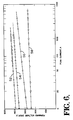
- a stainless steel base was used with a 75 ⁇ m thick layer of chromium. The device was found to exhibit a significantly lower forward voltage drop than prior devices when the cathode was coated with chromium, and an even lower forward voltage drop when both a chromium surface and cathode grooves were employed. These results are shown in the graph of FIG. 6, in which the forward voltage drop is plotted as a function of the peak cathode current.
- Trace 52 is a plot of the forward voltage drop for a smooth-walled cathode with a thoriated tungsten layer
- trace 54 is for a smooth-walled molybdenum coating
- trace 56 is for a smooth-walled chromium coating
- trace 58 is for a grooved cathode with a chromium coating.
- FIG. 2 demonstrates that the forward voltage drop scales in proportion to ⁇ w lnI p , where ⁇ w is the work function of the cold cathode material and I p is the peak current.
- the ratio of the forward voltage drops for smooth-bore thoriated tungsten, molybdenum and chromium is nearly equal to the ratio of their work functions.
- experimentation conducted in connection with the present invention has established chromium as having a high secondary electron yield, it does not suffer from the significant sputtering problem that plagued prior low work function cathode coatings.
- a chromium coating on the inner cathode surface also offers considerable advantages.
- a chromium layer can be formed on the cathode by a simple and inexpensive electroplating process.
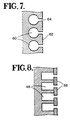
- FIGs. 7 and 8 Two such variations are illustrated in FIGs. 7 and 8, both involving the provision of annular cavities rather than grooves.
- a series of ring-shaped cavities 60 are formed in the cathode, and open to the interior cathode surface 62 through necks 64.
- the cathode grooves 48 are partially closed by a series of annular crossbars 66, which overlap the inner cathode surface between grooves and extend partially across the groove openings.
- the cavities would be coated with either chromium or a chromium mixture as discussed above.
- the openings from the cavities to the interior of the switch are substantially smaller than the inside dimensions of the cavities themselves, which serves to further increase the secondary electron path length and the consequent efficiency of the system.
Landscapes
- Gas-Filled Discharge Tubes (AREA)
Claims (9)
- Kaltkathode zum Schaffen einer Sekundärelektronemission zu einem benachbarten Plasma eines Kreuzfeld-Plasmaschalters, miteinem Kaltkathoden-Basisteil (2; 24), wobei eine Oberflächenschicht des Kathoden-Basisteils (2; 24) dem Plasma ausgesetzt ist, wobeieine Reihe von Strukturen (50) im Kathoden-Basisteil (2; 24) ausgebildet sind, welche den dem Plasma ausgesetzten, effektiven Oberflächeninhalt der Kathode im Vergleich zu einer glattwandigen Oberfläche vergrößern, und welche gestaltet sind, um die vom Kathoden-Basisteil (2; 24) emittierten Sekundärelektronen aufzuhalten, um die durchschnittliche effektive Weglänge der Sekundärelektronen durch das benachbarte Plasma zu erhöhen,dadurch gekennzeichnet, daß
die Oberflächenschicht des Kathoden-Basisteils (2; 24) aus zumindest 99% Chrom, aus einer Mischung von Chrom und Chromoxid oder aus einer Mischung von Chrom und einem Material, welches aus der Gruppe mit Wolfram, Molybdän und Thorium ausgewählt ist, ausgebildet ist. - Kaltkathode nach Anspruch 1, dadurch gekennzeichnet, daß das Kathoden-Basisteil (2; 24) aus einem anderen Material als Chrom ausgebildet ist, wobei die Oberflächenschicht auf dem Kathoden-Basisteil (2; 24) galvanisch aufgetragen ist.
- Kaltkathode nach Anspruch 1 oder 2, dadurch gekennzeichnet, daß die Strukturen (50) eine zur Reduzierung des Spannungsabfalls in Durchlaßrichtung des Plasmaschalters geeignete Tiefe aufweisen, während es dem Plasma ermöglicht ist, in die Strukturen (50) einzudringen.
- Kaltkathode nach Anspruch 3, dadurch gekennzeichnet, daß die Strukturen (50) eine Tiefe aufweisen, die größer als zweimal die Dicke eines Mantels der Kathode ist.
- Kaltkathode nach einem der Ansprüche 1 bis 4, dadurch gekennzeichnet, daß die Strukturen (50) eine Reihe von Nuten (48) mit im wesentlichen parallelen Seitenwänden aufweisen.
- Kaltkathode nach einem der Ansprüche 1 bis 5, dadurch gekennzeichnet, daß die Strukturen (50) im Kathoden-Basisteil (2; 24) Hohlräume (60) mit zum Plasma hinweisenden Öffnungen (64) aufweisen, welche im wesentlichen kleiner als das Innere der Hohlräume (60) sind (Fig. 7).
- Kaltkathode nach einem der Ansprüche 1 bis 5, dadurch gekennzeichnet, daß die Strukturen (50) im Kathoden-Basisteil (2; 24) aus Nuten (48) ausgebildete Hohlräume mit einer Reihe von Querschienen (66) enthalten, die die Kathodenoberfläche zwischen den Nuten (48) überlappen und die Nuten (48) teilweise schließen (Fig. 8).
- Kreuzfeld-Plasmaschalter, mit[a] einem Vakuumgehäuse;[b] einer Kaltkathode (2; 24) innerhalb dem Gehäuse, die eine Quelle für Sekundärelektronen ausbildet;[c] einer von der Kathode beabstandeten Anode (4; 26), wobei im Gehäuse ein Quellengitter (6; 28) zwischen der Anode und der Kathode angeordnet ist;[d] einer Einrichtung (46) zum Zuführen von ionisierbarem Gas in den Freiraum zwischen der Kathode und dem Quellengitter, wobei die Kathode und das Quellengitter im Ansprechen auf ein vorbestimmtes Spannungsdifferential zwischen der Kathode und dem Quellengitter zwischen sich ein Plasma aufrecht erhalten;[e] einem Steuergitter (8; 30), welches zwischen dem Quellengitter und der Anode zur wahlweisen Freigabe und zum Abschließen eines Plasmaweges zwischen der Kathode und der Anode angeordnet ist, wobei es den Schalter im Ansprechen auf vom Steuergitter zugeführte Steuerspannungssignale schließt und öffnet; und[f] einer Magneteinrichtung (10; 44), die das Plasma in einem vorbestimmten Bereich zwischen der Kathode und der Anode hält;dadurch gekennzeichnet, daß
[b1] die Kaltkathode (2; 24) nach einem der Ansprüche 1 bis 6 ausgebildet ist. - Kreuzfeld-Plasmaschalter nach Anspruch 8 und mit einer Kaltkathode nach Anspruch 5, wobei über einen Kathodenmantelbereich des Plasmas ein Spannungsdifferential zwischen der Kathode (2; 24) und dem Plasma existiert, dadurch gekennzeichnet, daß die Nuten im wesentlichen breiter als zweimal die Breite des Kathodenmantelbereiches sind.
Applications Claiming Priority (3)
| Application Number | Priority Date | Filing Date | Title |
|---|---|---|---|
| US07/207,603 US5019752A (en) | 1988-06-16 | 1988-06-16 | Plasma switch with chrome, perturbated cold cathode |
| US207603 | 1988-06-16 | ||
| PCT/US1989/001906 WO1989012905A1 (en) | 1988-06-16 | 1989-05-08 | Plasma switch with chrome, perturbated cold cathode |
Publications (2)
| Publication Number | Publication Date |
|---|---|
| EP0372072A1 EP0372072A1 (de) | 1990-06-13 |
| EP0372072B1 true EP0372072B1 (de) | 1996-08-28 |
Family
ID=22771256
Family Applications (1)
| Application Number | Title | Priority Date | Filing Date |
|---|---|---|---|
| EP89908112A Expired - Lifetime EP0372072B1 (de) | 1988-06-16 | 1989-05-08 | Plasma-schalter mit einer chrom-kathode mit strukturierter oberfläche |
Country Status (6)
| Country | Link |
|---|---|
| US (1) | US5019752A (de) |
| EP (1) | EP0372072B1 (de) |
| JP (1) | JPH0734349B2 (de) |
| DE (1) | DE68927043T2 (de) |
| IL (1) | IL90430A (de) |
| WO (1) | WO1989012905A1 (de) |
Families Citing this family (25)
| Publication number | Priority date | Publication date | Assignee | Title |
|---|---|---|---|---|
| GB8923123D0 (en) | 1989-10-13 | 1989-11-29 | Connaught Lab | A vaccine for human immunodeficiency virus |
| GB9007327D0 (en) * | 1990-03-31 | 1990-05-30 | Smiths Industries Plc | Gas discharge electrodes |
| US5212425A (en) * | 1990-10-10 | 1993-05-18 | Hughes Aircraft Company | Ion implantation and surface processing method and apparatus |
| US5132597A (en) * | 1991-03-26 | 1992-07-21 | Hughes Aircraft Company | Hollow cathode plasma switch with magnetic field |
| US5329205A (en) * | 1992-06-19 | 1994-07-12 | Hughes Aircraft Company | High voltage crossed-field plasma switch |
| GB2269700B (en) * | 1992-08-07 | 1996-03-06 | Smiths Industries Plc | Discharge lamps |
| GB9216785D0 (en) * | 1992-08-07 | 1992-09-23 | Smiths Industries Plc | Gas discharge electrodes |
| US5336975A (en) | 1992-10-20 | 1994-08-09 | Hughes Aircraft Company | Crossed-field plasma switch with high current density axially corrogated cathode |
| US5330800A (en) * | 1992-11-04 | 1994-07-19 | Hughes Aircraft Company | High impedance plasma ion implantation method and apparatus |
| DE4408941A1 (de) * | 1994-03-16 | 1995-09-21 | Licentia Gmbh | Vorratskathode |
| US5558718A (en) * | 1994-04-08 | 1996-09-24 | The Regents, University Of California | Pulsed source ion implantation apparatus and method |
| US5608297A (en) * | 1994-12-27 | 1997-03-04 | Hughes Electronics | Plasma switch and switching method with fault current interruption |
| US5640843A (en) * | 1995-03-08 | 1997-06-24 | Electric Propulsion Laboratory, Inc. Et Al. | Integrated arcjet having a heat exchanger and supersonic energy recovery chamber |
| JPH1046332A (ja) * | 1996-07-30 | 1998-02-17 | Nec Corp | 金属薄膜形成装置 |
| US5828176A (en) * | 1996-11-27 | 1998-10-27 | Hughes Electronics Corporation | Planar crossed-field plasma switch and method |
| US6417604B1 (en) * | 1996-12-12 | 2002-07-09 | Siemens Aktiengesellshaft | Low pressure gas discharge switch |
| US7163901B2 (en) | 2002-03-13 | 2007-01-16 | Varian Semiconductor Equipment Associates, Inc. | Methods for forming thin film layers by simultaneous doping and sintering |
| US6878415B2 (en) * | 2002-04-15 | 2005-04-12 | Varian Semiconductor Equipment Associates, Inc. | Methods for chemical formation of thin film layers using short-time thermal processes |
| US7994892B2 (en) * | 2007-06-21 | 2011-08-09 | Jpa Inc. | Oxidative opening switch assembly and methods |
| BR112015023115A2 (pt) * | 2013-03-15 | 2017-07-18 | Gen Electric | dispositivo comutador de catodo frio e conversor de potência |
| US10256067B1 (en) | 2018-01-02 | 2019-04-09 | General Electric Company | Low voltage drop, cross-field, gas switch and method of operation |
| US10665402B2 (en) | 2018-02-08 | 2020-05-26 | General Electric Company | High voltage, cross-field, gas switch and method of operation |
| US10403466B1 (en) | 2018-03-23 | 2019-09-03 | General Electric Company | Low sputtering, cross-field, gas switch and method of operation |
| WO2022099092A1 (en) * | 2020-11-06 | 2022-05-12 | The Regents Of The University Of California | Single phase high entropy intermetallics and method for manufacturing |
| JP7466789B2 (ja) * | 2021-09-09 | 2024-04-12 | 株式会社東芝 | スイッチング装置、直流遮断装置および直流遮断システム |
Citations (1)
| Publication number | Priority date | Publication date | Assignee | Title |
|---|---|---|---|---|
| EP0270876A2 (de) * | 1986-12-15 | 1988-06-15 | ELTRO GmbH Gesellschaft für Strahlungstechnik | Oberflächen für elektrische Entladungen |
Family Cites Families (8)
| Publication number | Priority date | Publication date | Assignee | Title |
|---|---|---|---|---|
| US1872359A (en) * | 1927-10-11 | 1932-08-16 | Westinghouse Electric & Mfg Co | Thermionic rectifier |
| US3596131A (en) * | 1969-05-29 | 1971-07-27 | Varian Associates | Cathode secondary emitter for crossed-field tubes |
| US4247804A (en) * | 1979-06-04 | 1981-01-27 | Hughes Aircraft Company | Cold cathode discharge device with grid control |
| US4394622A (en) * | 1981-06-03 | 1983-07-19 | Rink John P | High voltage coaxial switch |
| JPS6015708B2 (ja) * | 1981-09-04 | 1985-04-20 | 日本電信電話公社 | ドライエツチング装置 |
| US4611147A (en) * | 1984-04-05 | 1986-09-09 | The United States Of America As Represented By The United States Department Of Energy | Thermionic gas switch |
| US4596945A (en) * | 1984-05-14 | 1986-06-24 | Hughes Aircraft Company | Modulator switch with low voltage control |
| US4637853A (en) * | 1985-07-29 | 1987-01-20 | International Business Machines Corporation | Hollow cathode enhanced plasma for high rate reactive ion etching and deposition |
-
1988
- 1988-06-16 US US07/207,603 patent/US5019752A/en not_active Expired - Fee Related
-
1989
- 1989-05-08 EP EP89908112A patent/EP0372072B1/de not_active Expired - Lifetime
- 1989-05-08 JP JP1507633A patent/JPH0734349B2/ja not_active Expired - Lifetime
- 1989-05-08 WO PCT/US1989/001906 patent/WO1989012905A1/en not_active Ceased
- 1989-05-08 DE DE68927043T patent/DE68927043T2/de not_active Expired - Fee Related
- 1989-05-26 IL IL90430A patent/IL90430A/xx not_active IP Right Cessation
Patent Citations (1)
| Publication number | Priority date | Publication date | Assignee | Title |
|---|---|---|---|---|
| EP0270876A2 (de) * | 1986-12-15 | 1988-06-15 | ELTRO GmbH Gesellschaft für Strahlungstechnik | Oberflächen für elektrische Entladungen |
Non-Patent Citations (1)
| Title |
|---|
| Opening Switches, Guenter et al. Plenum Publishing 1987 pages 93-129"Low pressure plasma opening switches, R. Schumacher et al. * |
Also Published As
| Publication number | Publication date |
|---|---|
| WO1989012905A1 (en) | 1989-12-28 |
| JPH0734349B2 (ja) | 1995-04-12 |
| IL90430A0 (en) | 1990-01-18 |
| DE68927043T2 (de) | 1997-01-16 |
| JPH03500109A (ja) | 1991-01-10 |
| DE68927043D1 (de) | 1996-10-02 |
| US5019752A (en) | 1991-05-28 |
| EP0372072A1 (de) | 1990-06-13 |
| IL90430A (en) | 1993-05-13 |
Similar Documents
| Publication | Publication Date | Title |
|---|---|---|
| EP0372072B1 (de) | Plasma-schalter mit einer chrom-kathode mit strukturierter oberfläche | |
| Oks et al. | Development of plasma cathode electron guns | |
| EP0283519B1 (de) | Ionenerzeugende apparatur, dünnschichtbildende vorrichtung unter verwendung der ionenerzeugenden apparatur und ionenquelle | |
| US4710283A (en) | Cold cathode ion beam source | |
| CA2254677C (en) | Apparatus for sputtering or arc evaporation | |
| US4684848A (en) | Broad-beam electron source | |
| US4610770A (en) | Method and apparatus for sputtering | |
| US6664739B1 (en) | Enhanced electron emissive surfaces for a thin film deposition system using ion sources | |
| US4447732A (en) | Ion source | |
| Leung et al. | Optimization of H− production from a small multicusp ion source | |
| EP0200035B1 (de) | Elektronenstrahlquelle | |
| US4749912A (en) | Ion-producing apparatus | |
| US4104875A (en) | Ion prime mover | |
| EP0185074B1 (de) | Elektronenstrahlgesteuerter schalter von radialer gestaltung, der eine draht-ionenplasma-elektronenquelle verwendetund eine derartige electronenquelle | |
| US4703222A (en) | Hall accelerator with preionization discharge | |
| US4466242A (en) | Ring-cusp ion thruster with shell anode | |
| RU2167466C1 (ru) | Плазменный источник ионов и способ его работы | |
| JP2913186B2 (ja) | イオン源装置 | |
| US5072148A (en) | Dispenser cathode with emitting surface parallel to ion flow and use in thyratrons | |
| US5545947A (en) | Multiple surface high voltage structure for a gas discharge closing switch | |
| JPS6386864A (ja) | イオン源 | |
| CA1221468A (en) | Plasma cathode electron beam generating system | |
| Schumacher et al. | Low-pressure plasma opening switches | |
| JPH03266346A (ja) | イオン生成装置 | |
| GB2169131A (en) | Gas discharge devices |
Legal Events
| Date | Code | Title | Description |
|---|---|---|---|
| PUAI | Public reference made under article 153(3) epc to a published international application that has entered the european phase |
Free format text: ORIGINAL CODE: 0009012 |
|
| 17P | Request for examination filed |
Effective date: 19900207 |
|
| AK | Designated contracting states |
Kind code of ref document: A1 Designated state(s): CH DE FR GB IT LI SE |
|
| 17Q | First examination report despatched |
Effective date: 19910318 |
|
| GRAH | Despatch of communication of intention to grant a patent |
Free format text: ORIGINAL CODE: EPIDOS IGRA |
|
| GRAH | Despatch of communication of intention to grant a patent |
Free format text: ORIGINAL CODE: EPIDOS IGRA |
|
| GRAA | (expected) grant |
Free format text: ORIGINAL CODE: 0009210 |
|
| AK | Designated contracting states |
Kind code of ref document: B1 Designated state(s): CH DE FR GB IT LI SE |
|
| PG25 | Lapsed in a contracting state [announced via postgrant information from national office to epo] |
Ref country code: LI Effective date: 19960828 Ref country code: CH Effective date: 19960828 |
|
| REF | Corresponds to: |
Ref document number: 68927043 Country of ref document: DE Date of ref document: 19961002 |
|
| ET | Fr: translation filed | ||
| ITF | It: translation for a ep patent filed | ||
| PG25 | Lapsed in a contracting state [announced via postgrant information from national office to epo] |
Ref country code: SE Effective date: 19961128 |
|
| REG | Reference to a national code |
Ref country code: CH Ref legal event code: PL |
|
| PLBE | No opposition filed within time limit |
Free format text: ORIGINAL CODE: 0009261 |
|
| STAA | Information on the status of an ep patent application or granted ep patent |
Free format text: STATUS: NO OPPOSITION FILED WITHIN TIME LIMIT |
|
| 26N | No opposition filed | ||
| REG | Reference to a national code |
Ref country code: GB Ref legal event code: 732E |
|
| REG | Reference to a national code |
Ref country code: FR Ref legal event code: TP Ref country code: FR Ref legal event code: CD Ref country code: FR Ref legal event code: CA |
|
| REG | Reference to a national code |
Ref country code: GB Ref legal event code: IF02 |
|
| PGFP | Annual fee paid to national office [announced via postgrant information from national office to epo] |
Ref country code: FR Payment date: 20020411 Year of fee payment: 14 |
|
| PGFP | Annual fee paid to national office [announced via postgrant information from national office to epo] |
Ref country code: GB Payment date: 20020417 Year of fee payment: 14 |
|
| PGFP | Annual fee paid to national office [announced via postgrant information from national office to epo] |
Ref country code: DE Payment date: 20020423 Year of fee payment: 14 |
|
| PG25 | Lapsed in a contracting state [announced via postgrant information from national office to epo] |
Ref country code: GB Free format text: LAPSE BECAUSE OF NON-PAYMENT OF DUE FEES Effective date: 20030508 |
|
| PG25 | Lapsed in a contracting state [announced via postgrant information from national office to epo] |
Ref country code: DE Free format text: LAPSE BECAUSE OF NON-PAYMENT OF DUE FEES Effective date: 20031202 |
|
| GBPC | Gb: european patent ceased through non-payment of renewal fee |
Effective date: 20030508 |
|
| PG25 | Lapsed in a contracting state [announced via postgrant information from national office to epo] |
Ref country code: FR Free format text: LAPSE BECAUSE OF NON-PAYMENT OF DUE FEES Effective date: 20040130 |
|
| REG | Reference to a national code |
Ref country code: FR Ref legal event code: ST |
|
| PG25 | Lapsed in a contracting state [announced via postgrant information from national office to epo] |
Ref country code: IT Free format text: LAPSE BECAUSE OF NON-PAYMENT OF DUE FEES;WARNING: LAPSES OF ITALIAN PATENTS WITH EFFECTIVE DATE BEFORE 2007 MAY HAVE OCCURRED AT ANY TIME BEFORE 2007. THE CORRECT EFFECTIVE DATE MAY BE DIFFERENT FROM THE ONE RECORDED. Effective date: 20050508 |