EP0372767A1 - Contact électrique miniature à déplacement d'isolation - Google Patents
Contact électrique miniature à déplacement d'isolation Download PDFInfo
- Publication number
- EP0372767A1 EP0372767A1 EP89312234A EP89312234A EP0372767A1 EP 0372767 A1 EP0372767 A1 EP 0372767A1 EP 89312234 A EP89312234 A EP 89312234A EP 89312234 A EP89312234 A EP 89312234A EP 0372767 A1 EP0372767 A1 EP 0372767A1
- Authority
- EP
- European Patent Office
- Prior art keywords
- embossments
- sidewall
- edges
- contact terminal
- sidewalls
- Prior art date
- Legal status (The legal status is an assumption and is not a legal conclusion. Google has not performed a legal analysis and makes no representation as to the accuracy of the status listed.)
- Granted
Links
- 238000009413 insulation Methods 0.000 title claims abstract description 17
- 238000006073 displacement reaction Methods 0.000 title claims abstract description 16
- 239000000463 material Substances 0.000 claims abstract description 20
- 239000004020 conductor Substances 0.000 claims description 8
- 238000000034 method Methods 0.000 abstract description 4
- 230000000717 retained effect Effects 0.000 abstract 1
- 238000005520 cutting process Methods 0.000 description 4
- 238000004519 manufacturing process Methods 0.000 description 4
- 210000005069 ears Anatomy 0.000 description 3
- 230000002093 peripheral effect Effects 0.000 description 3
- 238000004049 embossing Methods 0.000 description 2
- 239000002184 metal Substances 0.000 description 2
- 229910000906 Bronze Inorganic materials 0.000 description 1
- 239000004677 Nylon Substances 0.000 description 1
- OAICVXFJPJFONN-UHFFFAOYSA-N Phosphorus Chemical compound [P] OAICVXFJPJFONN-UHFFFAOYSA-N 0.000 description 1
- 229910001315 Tool steel Inorganic materials 0.000 description 1
- 239000010974 bronze Substances 0.000 description 1
- KUNSUQLRTQLHQQ-UHFFFAOYSA-N copper tin Chemical compound [Cu].[Sn] KUNSUQLRTQLHQQ-UHFFFAOYSA-N 0.000 description 1
- 230000000694 effects Effects 0.000 description 1
- 230000008030 elimination Effects 0.000 description 1
- 238000003379 elimination reaction Methods 0.000 description 1
- 238000005304 joining Methods 0.000 description 1
- LQBJWKCYZGMFEV-UHFFFAOYSA-N lead tin Chemical compound [Sn].[Pb] LQBJWKCYZGMFEV-UHFFFAOYSA-N 0.000 description 1
- 230000014759 maintenance of location Effects 0.000 description 1
- 229920001778 nylon Polymers 0.000 description 1
- 238000007747 plating Methods 0.000 description 1
- 230000035939 shock Effects 0.000 description 1
- 230000006641 stabilisation Effects 0.000 description 1
- 238000011105 stabilization Methods 0.000 description 1
Images




Classifications
-
- H—ELECTRICITY
- H01—ELECTRIC ELEMENTS
- H01R—ELECTRICALLY-CONDUCTIVE CONNECTIONS; STRUCTURAL ASSOCIATIONS OF A PLURALITY OF MUTUALLY-INSULATED ELECTRICAL CONNECTING ELEMENTS; COUPLING DEVICES; CURRENT COLLECTORS
- H01R4/00—Electrically-conductive connections between two or more conductive members in direct contact, i.e. touching one another; Means for effecting or maintaining such contact; Electrically-conductive connections having two or more spaced connecting locations for conductors and using contact members penetrating insulation
- H01R4/24—Connections using contact members penetrating or cutting insulation or cable strands
-
- H—ELECTRICITY
- H01—ELECTRIC ELEMENTS
- H01R—ELECTRICALLY-CONDUCTIVE CONNECTIONS; STRUCTURAL ASSOCIATIONS OF A PLURALITY OF MUTUALLY-INSULATED ELECTRICAL CONNECTING ELEMENTS; COUPLING DEVICES; CURRENT COLLECTORS
- H01R4/00—Electrically-conductive connections between two or more conductive members in direct contact, i.e. touching one another; Means for effecting or maintaining such contact; Electrically-conductive connections having two or more spaced connecting locations for conductors and using contact members penetrating insulation
- H01R4/24—Connections using contact members penetrating or cutting insulation or cable strands
- H01R4/2416—Connections using contact members penetrating or cutting insulation or cable strands the contact members having insulation-cutting edges, e.g. of tuning fork type
- H01R4/2445—Connections using contact members penetrating or cutting insulation or cable strands the contact members having insulation-cutting edges, e.g. of tuning fork type the contact members having additional means acting on the insulation or the wire, e.g. additional insulation penetrating means, strain relief means or wire cutting knives
- H01R4/2466—Connections using contact members penetrating or cutting insulation or cable strands the contact members having insulation-cutting edges, e.g. of tuning fork type the contact members having additional means acting on the insulation or the wire, e.g. additional insulation penetrating means, strain relief means or wire cutting knives the contact members having a channel-shaped part, the opposite sidewalls of which comprise insulation-cutting means
Definitions
- This invention relates to a stamped and formed electrical contact terminal for establishing an insulation displacement contact with an insulated wire. More specifically, this invention relates to a terminal for establishing an interconnection between an insulated wire and a pin, such as a pin on a printed circuit board. Still more specifically, this invention relates to a stamped and formed electrical contact terminal in which an insulation displacement contact is formed by inserting an insulated conductor into a plate having a slot extending inwardly from one end, in which sidewalls of the terminal extend transversely past opposite edges of the plates.
- U.S. Patent 3,767,841 discloses one electrical connector employing slotted plates folded upwardly form the base to form a "U" shaped contact member. The edges of the slot formed in the two plates in this terminal penetrate the insulation surrounding the inner conductive core and establish a secure, gas-tight interconnection to the underlying conductive core. Contact is established by the use of multiple slotted plates.
- the connector shown in U.S. Patent 3,767,841 is a splice connector in which two or more wires are terminated to the same connector in one operation.
- This same slotted plate insulation displacement concept has been expanded to permit a large number of wires to be attached to separate terminals in a single insulative housing, all at the same time. This concept is generally referred to as mass termination.
- U.S. Patent 3,926,498 discloses a number of terminal configurations each of which can be positioned within a single insulative housing for mass termination. These terminals generally employ slotted plates which are either folded inwardly from side edges of a "U" shaped channel of a stamped and formed terminal, or are folded upwardly from the base of the channel shaped terminals, between opposed sidewalls.
- the various embodiments of the contact terminal shown in U.S. Patent 3,926,498 all disclose versions in which the slotted plates engage the sidewalls of the contacts. In these versions of contact terminals, ears are formed on the side edges of the slotted plates, and these slotted plates fit within cut-outs or slots located on the exterior of the sidewalls.
- a slotted plate supported in this manner by a "U” shaped member does not tend to collapse when a wire is inserted laterally in its axis into the slot.
- Contact terminals which use a "U” shaped member in which the slotted plates formed upwardly from the base of the "U” are held in engagement by sidewalls extending from the opposed edges of the base are also shown in PCT International Application WO 86/ 01941; U.S. Patent 4,545,634 and in Japanese UM Publication 60-142463.
- any material which is stamped out of a terminal of this type reduces the cross sectional area available to carry current.
- any material which is eliminated also reduces the surface area of the contact, thus reducing its ability to dissipate heat formed by the current passing through the terminal.
- any elimination of material also reduces the mechanical strength of such a terminal.
- This invention is related to a contact terminal for establishing an insulation displacement interconnection to an insulated conductor.
- This contact terminal includes at least one slotted plate which is secured to one or more sidewalls extending transversely past the slotted plate.
- the slotted plates are secured to the sidewalls by embossments formed in the sidewalls on opposite sides of the plates. Sheared edges of these embossments extend parallel to the opposite faces of the slotted plates and provide a secure engagement with a slotted plate.
- embossments can be formed by the use of dies without the necessity of employing thin blades to punch or stamp slots in the sidewall.
- these embossments are formed in the sidewalls without the necessity of removing material. Since the embossments extend outwardly from the plane of the sidewall, mechanical strength is added to the otherwise generally planar sidewalls. Thus a more secure and reliable insulation displacement interconnection can formed.
- the stamped and formed contact terminal 2 comprising the preferred embodiment of this inventor is intended for use in establishing an insulation displacement interconnection with insulated conductors 4 in the form of insulated wires.
- contact terminal 2 is also suitable for forming a resilient spring contact with a pin 6, such as a pin extending upwardly from a printed circuit board.
- a plurality of contact terminals 2 will normally be positioned within an insulative housing with contact terminals 2 being side by side so that the connector can be attached to a plurality of side by side pins 6.
- the contact terminal 2 can be stamped and formed from a conventional electrically-conductive spring metal such as phosphor bronze.
- This contact can be plated with a conventional material to enhance its conductive properties.
- a tin lead plating can be employed.
- the contact terminal has a uniform thickness of 0.008 inches.
- contact terminals formed in accordance with the preferred embodiment can be positioned in a multi-cavity housing 8 molded from a conventional insulative material such as nylon. In the preferred embodiment of this invention these contact terminals are to be employed in a connector in which adjacent terminals will be on 2.5 millimeter center lines.
- the insulation displacement contact termination to an insulated conductor 4 is formed by a pair of slotted plates 10A and 10B which have slots 12A and 12B extending inwardly from their free end.
- plates 10A and 10B are located side by side and parallel, with slots 12A and 12B being in alignment so that a multiple termination can be made to a single wire.
- Slots 12A and 12B extend parallel to flat or straight side edges 14A and 14B of the plates 10A and 10B. Since the contact terminal 2 is formed from a material having uniform thickness, thickness of plates 10A and 10B is the same as the thickness of the remaining portion of contact terminal 2.
- Outer and inner faces 18A and 18B of each plate 10A and 10B extend generally perpendicular to the axis of an insulative conductor 4 terminated within the insulation displacement slots 12A and 12B.
- Sidewalls 20A and 20B extend transversely past both plates 10A and 10B with the straight side edges 14A and 14B of each plate being juxtaposed and close to the interior surface of the sidewalls. Indeed, in the preferred embodiment of this invention the straight side edges 14A and 14B of the plates will almost, but not necessarily, touch the interior surface of the sidewalls.
- Each of the sidewalls 20A and 20B is joined to a common base 24 between the plates 10A and 10B. Plates 10A and 10B are stamped from portions of the flat blank used in the fabrication of this terminal which would otherwise comprise longitudinal extensions of the common base 24. Plates 10A and 10B are folded upwardly from the common base 24 to leave two rectangular openings in the plane of the base 24.
- the sidewalls 20A and 20B are formed orthogonally upwardly from opposite radiused edges 26 joining the common base 24.
- the sidewalls 20A and 20B are generally planar.
- Embossments 28, 30A, and 30B are formed outwardly from planar sections of sidewalls 20A and 20B by an embossing or shallow drawing process in which the metal flows during the process of forming the embossments.
- Outer embossments 30A and 30B are located adjacent opposite ends of a central embossment 28.
- a strap 22, which forms that portion of the sidewalls immediately juxtaposed to the side edges 14A and 14B remains between adjacent sheared edges 32 of embossment 28, 30A, and 30B.
- a strap 22 will be located at each end of the central embossment 28, respectively between the central embossment 28 and the adjacent outer embossments 30A and 30B.
- the central cylindrical embossment 28 has first sheared edges 32 at opposite longitudinal ends of the generally cylindrical shaped embossment and peripheral edges 34 joined to the sidewalls above and below the sheared edges and extending between the ends of the central embossment 28A on which the first sheared edges 32 are formed.
- Each of the outer embossments 30A and 30B has only a single sheared edge 32, with a continuous peripheral edge 34 extending arcuately between the upper and lower ends of the sheared edge 32.
- the outer embossment 30A and 30B have a generally ellipsoidal shape.
- Peripheral edges 34 on outer embossments 30A and 30B are generally curved and the sheared edge 32 on outer embossments 30A and 30B forms a straight projection in the plane of the sidewalls 20A and 20B. Since the sidewalls 20A and 20B are formed upwardly around the common base 24 to form a generally channel shaped configuration, the convex inner surface 36 of the embossments 28, 30A and 30B, will be located on the inner surface of the sidewalls 20A and 20B. Concave outer surfaces 38 will in turn be located on the exterior of the sidewalls 20A and 20B.
- the sheared edges 32 of the central embossment 28 and the outer embossments 30A and 30B will be positioned so that they will be flush with the faces 18A and 18B of the plates 10A and 10B.
- the embossments 28, 30A and 30B will form nests to securely retain the plates 10A and 10B in their upright positions between the sidewalls 20A and 20B.
- the contact terminal 2 also includes a pin contact section 40 at one end and strain relief section 50 at the other end of the termination section.
- the pin contact section 40 includes a base section 42 which is in the same plane and spaced from the common base 24 by the cut-outs formed when plates 10A and 10B are formed upwardly.
- Spring contact arms 44A and 44B extend upwardly from opposite side edges of the base section 42.
- the spring contact arms 44A and 44B include outwardly bowed sections 46A and 46B adjacent the base section 42 which merge with inclined straight sections 48A and 48B extending between the outwardly bowed sections in the free end of the spring contact arms.
- the straight sections are configured to establish an interconnection with a round or a square pin which is inserted into the pin contact through the front of the contact terminal 2.
- Tapered lead in sections 49 located on the lateral edge of straight sections 48A and 48B permit a pin 6 to enter without stubbing against the spring contact arms 44A and 44B.
- Spring contact arms are inclined so that pins of different sizes and cross-sectional configurations can be accommodated. By angling the contact arms inwardly, the interface point between the pin and the contact arms is maintained at a relatively high distance above the base of the contact thus avoiding overstressing of the contact material.
- Strain relief arms 52A and 52B are spaced from the termination section on the opposite end of the contact terminal 2 from the pin contact section 40. These strain relief arms can be crimped or deformed around a wire inserted into the slots 12A and 12B and serve to hold the wire firmly in place.
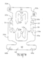
- Figures 8 and 9 depict the manner in which the contact terminal 2 is stamped and formed and in which the embossments 28, 30A and 30B are formed.
- the embossments 28, 30A and 30B are formed in a blank stock 60 before the contact terminal is profiled. These embossments are formed prior to profiling because each involves a shallow drawing or embossing process which causes material to flow laterally in the plane of the blank stock. If the outer profile of the contact terminal 2 were formed before the embossment 28, 30A and 30B were formed, the outer profile of the contact terminal would be altered. It should be understood, however, that such deformation of the outer profile of the contact terminal would not affect the performance of contact terminal 2 and would be otherwise suitable for use.
- Embossments 30A and 30B are initially formed by the engagement of convex ellipsoidal shear inserts 62 with a blank stock 60. These ellipsoidal shear inserts 62 protrude above the flat surface of the lower die and have a generally arcuate or curved outer surface extending from the apex to a flat cutting edge which forms the shear lines at the edges of the outer embossments 30A and 30B.
- Punch 65 is insertable between the shear inserts 62 and engages a flat surface around which these shear inserts 62 protrude. The flat shock is sheared where the flat cutting edges of the inserts 62 are closely adjacent and conform to the outline of the punch 65. Note that these shear lines and the embossments 30A and 30B are formed without the use of thin, fragile cutting blades.
- the central embossments 28 are formed by the engagement of cylindrical inserts 64 with punch 66 at station B.
- a pair of cylindrical convave depressions 66B are formed in the in the working face of punch 66.
- An insert 66C having punch ribs 66A in positioned within punch 66. Portions of the punch ribs 66A extend across the cylindrical depressions 66B.
- Punch ribs 66A are positioned on the punch to extend between cylindrical inserts 64 and the previously formed ellipsiodal embossments 30A and 30B.
- the punch insert 66C comprises a relatively long tool steel rod which is received within the outer portion 66D of punch 66. Punch ribs 66A thus do not extend beyond the flat working face of the punch. Thus the ribs 66A do not constitute fragile cutting blades which would be subject to damage.
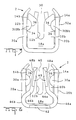
- the plate 10A and 10B can be profiled by the use of a relatively large punch which need not use a plurality of fragile blades to punch through the stock. Since the opening 68 must be cut out of the blank and the material disposed of, the punch which forms these openings must extend downward through the material and the height of this punch must be significantly greater than the height of punch rib 66A. Thus, a small, thin blade which would be used to cut material away from plate sections of prior art devices having locking ears integral with the slotted plate, of the type shown in Figures 11A and 11B would be unnecessary. Furthermore, it is not necessary to shear the outer portion of the ears away from the sidewalls as would be necessary in the fabrication of the prior art type contacts as shown in Figures 11A and 11B.
- the retention and stabilization embossments 28, 30A and 30B serve to stabilize the insulation displacement plates 10A and 10B during termination of an insulated conductor.
- This structure also provides greater mechanical integrity and a stronger connection between the front and back ends of the contact than is possible when material must be removed.
- additional material is available to transmit heat generated by the electrical current, thus eliminating potential hot spots and resulting in a better current rating for the contact.
- the sheared edge of the embossment 30A and 30B also provide a positive stop for the IDC blades or contacts and increase the strength of terminal if subjected to tensile force by the wire.
- the current invention provides a contact terminal which is both simpler and more efficient to fabricate and which provides increased performance.
- the current invention is especially adapted for use with relatively small terminals, where there is little material in the contact terminal available for the fabrication of structural elements of the connector, it is also possible to use the same configuration with larger contacts.
- the current invention is intended for use with 24AWG wire, although it is understood that contact terminals employing the same basic invention would be suitable for use with larger wire.
Landscapes
- Coupling Device And Connection With Printed Circuit (AREA)
- Manufacturing Of Electrical Connectors (AREA)
- Connections Arranged To Contact A Plurality Of Conductors (AREA)
- Connections By Means Of Piercing Elements, Nuts, Or Screws (AREA)
Applications Claiming Priority (2)
| Application Number | Priority Date | Filing Date | Title |
|---|---|---|---|
| US280753 | 1988-12-06 | ||
| US07/280,753 US4948382A (en) | 1988-12-06 | 1988-12-06 | Miniature insulation displacement electrical contact |
Publications (2)
| Publication Number | Publication Date |
|---|---|
| EP0372767A1 true EP0372767A1 (fr) | 1990-06-13 |
| EP0372767B1 EP0372767B1 (fr) | 1994-10-12 |
Family
ID=23074483
Family Applications (1)
| Application Number | Title | Priority Date | Filing Date |
|---|---|---|---|
| EP89312234A Expired - Lifetime EP0372767B1 (fr) | 1988-12-06 | 1989-11-24 | Contact électrique miniature à déplacement d'isolation |
Country Status (8)
| Country | Link |
|---|---|
| US (1) | US4948382A (fr) |
| EP (1) | EP0372767B1 (fr) |
| JP (1) | JP2897041B2 (fr) |
| KR (1) | KR970011881B1 (fr) |
| CN (1) | CN1029894C (fr) |
| DE (1) | DE68918814T2 (fr) |
| MX (1) | MX162504A (fr) |
| MY (1) | MY104257A (fr) |
Cited By (3)
| Publication number | Priority date | Publication date | Assignee | Title |
|---|---|---|---|---|
| EP0549957A3 (en) * | 1991-12-30 | 1993-12-22 | Molex Inc | Terminal locking means for electrical connectors |
| EP0613211A1 (fr) * | 1993-02-25 | 1994-08-31 | The Whitaker Corporation | Assemblage de contact à déplacement d'isolation pour connecteur électrique |
| EP0845836A1 (fr) * | 1996-12-02 | 1998-06-03 | Sumitomo Wiring Systems, Ltd. | Organe de contact |
Families Citing this family (13)
| Publication number | Priority date | Publication date | Assignee | Title |
|---|---|---|---|---|
| JPH0734373B2 (ja) * | 1989-11-15 | 1995-04-12 | ヒロセ電機株式会社 | コネクタ |
| DE4102436C2 (de) * | 1991-01-28 | 1996-12-19 | Siemens Ag | Vorrichtung zur elektrischen Verbindung mehrerer Leitungen |
| DE4207369C1 (fr) * | 1992-03-04 | 1993-07-29 | Krone Ag, 1000 Berlin, De | |
| JP2885258B2 (ja) * | 1992-09-11 | 1999-04-19 | 矢崎総業株式会社 | 圧接端子金具 |
| KR950012819A (ko) * | 1993-10-29 | 1995-05-17 | 프랭크 에이. 우울풀링 | 전기컨넥터 |
| JP3802153B2 (ja) * | 1996-08-08 | 2006-07-26 | 矢崎総業株式会社 | 圧接端子 |
| JP3242846B2 (ja) * | 1996-09-03 | 2001-12-25 | 矢崎総業株式会社 | 圧接端子 |
| JP2000348786A (ja) * | 1999-06-04 | 2000-12-15 | Sumitomo Wiring Syst Ltd | 圧接端子金具 |
| JP2001229988A (ja) * | 2000-02-21 | 2001-08-24 | Yazaki Corp | 圧接端子 |
| US6746268B2 (en) * | 2001-12-05 | 2004-06-08 | Tyco Electronics Corporation | Coaxial cable displacement contact |
| EP2124295A3 (fr) * | 2008-05-24 | 2011-03-30 | Lumberg Connect GmbH | Contact électrique |
| CA2935749A1 (fr) * | 2014-01-07 | 2015-07-16 | Minipumps, Llc | Rondelles de soudage pour soudage par microfil |
| JP6796621B2 (ja) * | 2018-07-06 | 2020-12-09 | 矢崎総業株式会社 | 電線と端子の接続構造の製造方法及び電線と端子の接続構造の製造方法に使用される端子 |
Citations (4)
| Publication number | Priority date | Publication date | Assignee | Title |
|---|---|---|---|---|
| US3993391A (en) * | 1975-09-19 | 1976-11-23 | Itt Industries, Inc. | Electrical contact for stripless cable connections |
| US4050760A (en) * | 1976-02-10 | 1977-09-27 | Trw Inc. | Solderless electrical contact |
| FR2454191A1 (fr) * | 1979-04-10 | 1980-11-07 | Cit Alcatel | Connecteur electrique |
| EP0063206A2 (fr) * | 1981-04-16 | 1982-10-27 | Grote & Hartmann GmbH & Co. KG | Contact à serrage |
Family Cites Families (13)
| Publication number | Priority date | Publication date | Assignee | Title |
|---|---|---|---|---|
| US3320354A (en) * | 1965-02-15 | 1967-05-16 | Amp Inc | Insulation piercing electrical connection |
| US3767841A (en) * | 1972-07-25 | 1973-10-23 | Amp Inc | Conductor in-slot electrical connectors |
| US3823392A (en) * | 1972-09-05 | 1974-07-09 | Heyman Mfg Co | Female contact blade |
| US3926498A (en) * | 1972-09-14 | 1975-12-16 | Bunker Ramo | Electrical connector and insulation-piercing contact member |
| US4324450A (en) * | 1980-03-05 | 1982-04-13 | Amp Inc. | Drop wire terminal |
| US4435035A (en) * | 1981-03-31 | 1984-03-06 | Amp Incorporated | Mass terminatable single row connector assembly |
| JPS5894291U (ja) * | 1981-12-19 | 1983-06-25 | 日本圧着端子製造株式会社 | 圧接形電気コネクタ |
| JPS6037814Y2 (ja) * | 1981-12-19 | 1985-11-11 | 日本圧着端子製造株式会社 | 圧接形電気コネクタの接触子 |
| JPS60142463A (ja) * | 1983-12-29 | 1985-07-27 | Fujitsu Ltd | かな漢字変換装置 |
| US4591230A (en) * | 1984-06-29 | 1986-05-27 | Frank Roldan | Electrical connector receptacle |
| JPS62135357U (fr) * | 1986-02-19 | 1987-08-26 | ||
| FR2604565B1 (fr) * | 1986-09-30 | 1990-02-09 | Amp France | Connecteur electrique et borne pour ce connecteur |
| JPS63164178A (ja) * | 1986-12-25 | 1988-07-07 | ヒロセ電機株式会社 | 電気接触子 |
-
1988
- 1988-12-06 US US07/280,753 patent/US4948382A/en not_active Expired - Fee Related
-
1989
- 1989-11-01 MY MYPI89001526A patent/MY104257A/en unknown
- 1989-11-21 MX MX18429A patent/MX162504A/es unknown
- 1989-11-24 DE DE68918814T patent/DE68918814T2/de not_active Expired - Fee Related
- 1989-11-24 EP EP89312234A patent/EP0372767B1/fr not_active Expired - Lifetime
- 1989-12-05 KR KR1019890017948A patent/KR970011881B1/ko not_active Expired - Fee Related
- 1989-12-05 CN CN89109166A patent/CN1029894C/zh not_active Expired - Fee Related
- 1989-12-06 JP JP1315532A patent/JP2897041B2/ja not_active Expired - Fee Related
Patent Citations (4)
| Publication number | Priority date | Publication date | Assignee | Title |
|---|---|---|---|---|
| US3993391A (en) * | 1975-09-19 | 1976-11-23 | Itt Industries, Inc. | Electrical contact for stripless cable connections |
| US4050760A (en) * | 1976-02-10 | 1977-09-27 | Trw Inc. | Solderless electrical contact |
| FR2454191A1 (fr) * | 1979-04-10 | 1980-11-07 | Cit Alcatel | Connecteur electrique |
| EP0063206A2 (fr) * | 1981-04-16 | 1982-10-27 | Grote & Hartmann GmbH & Co. KG | Contact à serrage |
Cited By (4)
| Publication number | Priority date | Publication date | Assignee | Title |
|---|---|---|---|---|
| EP0549957A3 (en) * | 1991-12-30 | 1993-12-22 | Molex Inc | Terminal locking means for electrical connectors |
| EP0613211A1 (fr) * | 1993-02-25 | 1994-08-31 | The Whitaker Corporation | Assemblage de contact à déplacement d'isolation pour connecteur électrique |
| US5427545A (en) * | 1993-02-25 | 1995-06-27 | The Whitaker Corporation | Insulation displacement electrical terminal assembly |
| EP0845836A1 (fr) * | 1996-12-02 | 1998-06-03 | Sumitomo Wiring Systems, Ltd. | Organe de contact |
Also Published As
| Publication number | Publication date |
|---|---|
| DE68918814D1 (de) | 1994-11-17 |
| US4948382A (en) | 1990-08-14 |
| MX162504A (es) | 1991-05-14 |
| MY104257A (en) | 1994-02-28 |
| CN1043226A (zh) | 1990-06-20 |
| CN1029894C (zh) | 1995-09-27 |
| EP0372767B1 (fr) | 1994-10-12 |
| JPH02195665A (ja) | 1990-08-02 |
| KR970011881B1 (ko) | 1997-07-18 |
| JP2897041B2 (ja) | 1999-05-31 |
| KR900011076A (ko) | 1990-07-11 |
| DE68918814T2 (de) | 1995-05-18 |
Similar Documents
| Publication | Publication Date | Title |
|---|---|---|
| US4261629A (en) | Slotted plate terminal | |
| US4948382A (en) | Miniature insulation displacement electrical contact | |
| EP0337659B1 (fr) | Système de retenue de broches de brasage | |
| JPH0713180Y2 (ja) | 電気コネクタ | |
| US5588884A (en) | Stamped and formed contacts for a power connector | |
| US4292736A (en) | Method for making jack type receptacles | |
| US4618207A (en) | Two piece modular receptacle | |
| CA1146231A (fr) | Connecteur pour boitier de prise electrique | |
| CA1088172A (fr) | Connecteur universelle, sans soudure | |
| US4527857A (en) | Terminal for connecting a wire to a blade type terminal | |
| EP3582332B1 (fr) | Borne de raccordement et structure de raccordement de borne | |
| EP0321285A1 (fr) | Borne bidirectionnelle, pour contacts électriques, à déplacement de l'isolation | |
| EP0607902B1 (fr) | Assemblage à bornes électriques reliées l'une à l'autre | |
| JPS5951491A (ja) | リブケ | |
| EP0191539B1 (fr) | Borne de connexion électrique pour connecteur | |
| JP3970321B2 (ja) | 電線接続システム | |
| JP3463900B2 (ja) | 電気コネクタ及びその製造方法 | |
| EP0876693B1 (fr) | Bloc de connexion pour cables | |
| US4109991A (en) | Self-stripping electrical connector and terminal | |
| EP0109297B1 (fr) | Eléments de contacts électriques et d'assemblages de connecteurs électriques | |
| US4264118A (en) | Insulation-pierce and crimp termination and method for effecting same | |
| EP0009867B1 (fr) | Douille électrique capable de recevoir une fiche électrique et méthode pour fabriquer cette douille | |
| US2811705A (en) | Electrical connector | |
| US5014535A (en) | Apparatus for forming embossments on electrical contact terminals | |
| JP2862433B2 (ja) | 電線用接続端子及び該端子用接続部品 |
Legal Events
| Date | Code | Title | Description |
|---|---|---|---|
| PUAI | Public reference made under article 153(3) epc to a published international application that has entered the european phase |
Free format text: ORIGINAL CODE: 0009012 |
|
| AK | Designated contracting states |
Kind code of ref document: A1 Designated state(s): DE FR GB IT NL |
|
| 17P | Request for examination filed |
Effective date: 19901124 |
|
| RAP1 | Party data changed (applicant data changed or rights of an application transferred) |
Owner name: THE WHITAKER CORPORATION |
|
| 17Q | First examination report despatched |
Effective date: 19930521 |
|
| GRAA | (expected) grant |
Free format text: ORIGINAL CODE: 0009210 |
|
| AK | Designated contracting states |
Kind code of ref document: B1 Designated state(s): DE FR GB IT NL |
|
| REF | Corresponds to: |
Ref document number: 68918814 Country of ref document: DE Date of ref document: 19941117 |
|
| ET | Fr: translation filed | ||
| ITF | It: translation for a ep patent filed | ||
| PLBE | No opposition filed within time limit |
Free format text: ORIGINAL CODE: 0009261 |
|
| STAA | Information on the status of an ep patent application or granted ep patent |
Free format text: STATUS: NO OPPOSITION FILED WITHIN TIME LIMIT |
|
| 26N | No opposition filed | ||
| PGFP | Annual fee paid to national office [announced via postgrant information from national office to epo] |
Ref country code: GB Payment date: 19971007 Year of fee payment: 9 |
|
| PGFP | Annual fee paid to national office [announced via postgrant information from national office to epo] |
Ref country code: FR Payment date: 19971106 Year of fee payment: 9 |
|
| PGFP | Annual fee paid to national office [announced via postgrant information from national office to epo] |
Ref country code: DE Payment date: 19971127 Year of fee payment: 9 |
|
| PGFP | Annual fee paid to national office [announced via postgrant information from national office to epo] |
Ref country code: NL Payment date: 19980914 Year of fee payment: 10 |
|
| PG25 | Lapsed in a contracting state [announced via postgrant information from national office to epo] |
Ref country code: GB Free format text: LAPSE BECAUSE OF NON-PAYMENT OF DUE FEES Effective date: 19981124 |
|
| GBPC | Gb: european patent ceased through non-payment of renewal fee |
Effective date: 19981124 |
|
| PG25 | Lapsed in a contracting state [announced via postgrant information from national office to epo] |
Ref country code: FR Free format text: LAPSE BECAUSE OF NON-PAYMENT OF DUE FEES Effective date: 19990730 |
|
| REG | Reference to a national code |
Ref country code: FR Ref legal event code: ST |
|
| PG25 | Lapsed in a contracting state [announced via postgrant information from national office to epo] |
Ref country code: DE Free format text: LAPSE BECAUSE OF NON-PAYMENT OF DUE FEES Effective date: 19990901 |
|
| PG25 | Lapsed in a contracting state [announced via postgrant information from national office to epo] |
Ref country code: NL Free format text: LAPSE BECAUSE OF NON-PAYMENT OF DUE FEES Effective date: 20000601 |
|
| NLV4 | Nl: lapsed or anulled due to non-payment of the annual fee |
Effective date: 20000601 |
|
| PG25 | Lapsed in a contracting state [announced via postgrant information from national office to epo] |
Ref country code: IT Free format text: LAPSE BECAUSE OF NON-PAYMENT OF DUE FEES;WARNING: LAPSES OF ITALIAN PATENTS WITH EFFECTIVE DATE BEFORE 2007 MAY HAVE OCCURRED AT ANY TIME BEFORE 2007. THE CORRECT EFFECTIVE DATE MAY BE DIFFERENT FROM THE ONE RECORDED. Effective date: 20051124 |