EP0373377A1 - Kratzfester Gebrauchsgegenstand sowie Verfahren zu seiner Herstellung - Google Patents
Kratzfester Gebrauchsgegenstand sowie Verfahren zu seiner Herstellung Download PDFInfo
- Publication number
- EP0373377A1 EP0373377A1 EP89121118A EP89121118A EP0373377A1 EP 0373377 A1 EP0373377 A1 EP 0373377A1 EP 89121118 A EP89121118 A EP 89121118A EP 89121118 A EP89121118 A EP 89121118A EP 0373377 A1 EP0373377 A1 EP 0373377A1
- Authority
- EP
- European Patent Office
- Prior art keywords
- silicon
- carbon
- glow discharge
- holder
- workpiece
- Prior art date
- Legal status (The legal status is an assumption and is not a legal conclusion. Google has not performed a legal analysis and makes no representation as to the accuracy of the status listed.)
- Granted
Links
Images
Classifications
-
- A—HUMAN NECESSITIES
- A47—FURNITURE; DOMESTIC ARTICLES OR APPLIANCES; COFFEE MILLS; SPICE MILLS; SUCTION CLEANERS IN GENERAL
- A47J—KITCHEN EQUIPMENT; COFFEE MILLS; SPICE MILLS; APPARATUS FOR MAKING BEVERAGES
- A47J36/00—Parts, details or accessories of cooking-vessels
- A47J36/02—Selection of specific materials, e.g. heavy bottoms with copper inlay or with insulating inlay
-
- C—CHEMISTRY; METALLURGY
- C23—COATING METALLIC MATERIAL; COATING MATERIAL WITH METALLIC MATERIAL; CHEMICAL SURFACE TREATMENT; DIFFUSION TREATMENT OF METALLIC MATERIAL; COATING BY VACUUM EVAPORATION, BY SPUTTERING, BY ION IMPLANTATION OR BY CHEMICAL VAPOUR DEPOSITION, IN GENERAL; INHIBITING CORROSION OF METALLIC MATERIAL OR INCRUSTATION IN GENERAL
- C23C—COATING METALLIC MATERIAL; COATING MATERIAL WITH METALLIC MATERIAL; SURFACE TREATMENT OF METALLIC MATERIAL BY DIFFUSION INTO THE SURFACE, BY CHEMICAL CONVERSION OR SUBSTITUTION; COATING BY VACUUM EVAPORATION, BY SPUTTERING, BY ION IMPLANTATION OR BY CHEMICAL VAPOUR DEPOSITION, IN GENERAL
- C23C16/00—Chemical coating by decomposition of gaseous compounds, without leaving reaction products of surface material in the coating, i.e. chemical vapour deposition [CVD] processes
- C23C16/22—Chemical coating by decomposition of gaseous compounds, without leaving reaction products of surface material in the coating, i.e. chemical vapour deposition [CVD] processes characterised by the deposition of inorganic material, other than metallic material
- C23C16/30—Deposition of compounds, mixtures or solid solutions, e.g. borides, carbides, nitrides
- C23C16/32—Carbides
Definitions
- the invention relates to a scratch-resistant commodity, in particular roasting or cooking utensils, processes for its production and devices for carrying out these processes.
- the invention has the sheep of scratch-resistant utensils, in particular roasting or cooking utensils.
- This object is achieved according to the invention in that it is provided on the surface with a carbon or silicon hard material layer.
- the core idea of the invention is the application of a layer which has a high level of hardness and tightness, that is to say freedom from pores and grain boundaries, and at the same time a great adhesive strength to the objects to be coated.
- the food to be roasted, baked or boiled should not be attached.
- the application of the inventive concept is possible for a wide variety of both metallic and non-metallic objects. Frying pans, saucepans, baking tins or even punching or forming tools are particularly suitable for this. Basically, carbon adheres only slightly to some materials, which include some metals, but above all steel and ceramics.
- the carbon has a regular additional hydrogen content of about 1 to 50 atomic percent.
- the invention is based on the completely unexpected finding that even small admixtures of possibly just a few percent silicon to carbon are sufficient to significantly increase the adhesion of this layer.
- the mechanical properties of the layer are not adversely affected.
- a further significant advantage has been shown here that the contact angle of the water drops on these layers compared to the pure made of amorphous carbons increased from a value of approximately below 70 degrees to over 110 degrees.
- a significant improvement in the water-repellent effect is observed. This hydrophobic behavior is all the more astonishing, since such effects are observed almost only with carbon and fluorine-containing materials, such as with the known PTFE (Teflon).
- the known method of plasma-activated chemical vapor deposition (PACVD, PCVD) is proposed as a method for producing the hard material layers on the articles of daily use.
- a glow discharge (synonymous with plasma) creates an ion bombardment of the object, which creates a hard, electrically insulating carbon layer with diamond-like properties.
- the glow discharge could be optimized with heating, which is called plasma-assisted CVD.
- the parts to be coated are heated to temperatures of several 100 to over 1000 degrees.
- Such a process also called pyrolysis, can be used in one Separate the hydrocarbon atmosphere Carbon, which, however, then has graphite-like properties, i.e. is soft, opaque and electrically conductive.
- glow discharge also requires gas from a pressure range of ten thousandths to a few mbar within the coating chamber. During the process of independent glow discharge, the gas is partially chemically excited, ionized and, in the case of multi-atomic gases, dissociated and broken down into radicals.
- the remaining atoms or molecules remain neutral.
- Compounds containing silicon and carbon are used as gases.
- it can be a gas from the large group of organosilicon compounds.
- liquids can also be used whose vapor pressure is often so high already at room temperature that they are sucked into the coating chamber by the vacuum alone.
- Particularly suitable gases are proposed Silane, tetrafluorocarbon, tetramethylsilane, hexamethyldisilane, hexamethyldisiloxane, hexamethyldisilazane, vinyldimethylethoxysilane, tetraethoxysilane or any other siloxanes, silazanes or silanes containing methyl, vinyl, phenyl or alkoxy groups.
- This also includes the halogenated equations such as dichloromethylsilane and trifluorosilane. It is important that sufficient hydrogen is added when halogens are present. Otherwise one would get the undesired plasma chemical etching.
- etching can be expected in a wide range of electrical power and gas pressure, whereas when replacing tetrachlorosilane with silane, a gas layer similar to SiC is formed from this gas mixture.
- the hydrogen combines with the fluorine to form HF gas, which is removed by the pumps. It is irrelevant to the invention in which molecular structure the process gases are present, whether they are linear, branched or ring-shaped structures. The molecules lose their original structure when they impact the sample holder or the workpiece to be coated there. It is also possible to use inorganic gases, such as silane or tetrafluorosilane, as silicon donors.
- the recipient wall forms one and the workpiece with the holder form the other electrode for generating the glow discharge and are connected to a high-frequency generator and have an evacuation device.
- there is an electrically insulated connection in the electrically conductive chamber which creates the connection between the sample holder and an external high-frequency generator with an upstream impedance converter, which together form the electrical energy supply.
- the interior of the chamber is connected via a connecting channel to a pump which is able to produce a vacuum with a pressure below one millibar.
- the process can still be carried out even with an increase in the background pressure and with lower pumping capacities, since the higher residual gas pressures then present, because of the high affinity of the silicon, allow the oxygen from the residual gas to be incorporated into the layers.
- This tolerance limit is only exceeded when the silicon organic agent used to form the layer oxidizes to such an extent that the layer no longer consists of silicon carbon, but quartz, that is to say silicon dioxide. Because of the extremely hydrophilic behavior of the silicon oxide, the desired non-stick effect is lost.
- the recipient wall consists of electrically insulating material, in which electrical fields serving to generate the glow discharge can be coupled in, for which purpose coils, internal / external electrodes or else a microwave cavity resonator are used. Since extremely hard, carbon-containing layers are only obtained when the workpiece is placed on a sample holder that is negatively polarized relative to the plasma, it is recommended to either apply a DC voltage to the sample holder or to connect a high-frequency generator.
- the sample holder and the workpiece connected to it in an electrically conductive manner become negatively charged over time due to the different mobility of electrons and ions originating from the plasma, provided the high-frequency generator is decoupled from the sample holder in terms of DC voltage, for example via a capacitor.
- the use of high frequency is indispensable for the production of electrically insulating carbon-containing layers with thicknesses of more than about 0.5 micrometers, since in the case of the use of direct voltage above the critical thickness, insulating layers are formed which are still too small with regard to the protection of the surface are and interrupt the current flow of electrons and ions and thus switch off the coating process.
- the use of direct voltage to achieve higher thicknesses presupposes that the gas mixture is selected so that the layer produced has the required electrical conductivity.
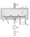
- a holder (4) with a workpiece (5) arranged thereon is located in the interior space delimited by the recipient wall (1). It is connected via an electrically insulated bushing (3) via the impedance converter (6) to a high-frequency generator (7) for the electrical energy supply.
- Glow discharges take place in the space delimited by the workpiece (5) and part of the recipient wall (1), which is delimited in the drawing with a dotted line, by means of which the layers containing carbon and silicon are deposited on the surface of the workpiece.
- the interior is evacuated with the help of the tube (8) via a device (not shown here) to such an extent that an independent glow discharge is formed, ie that the gas is partially chemically excited, ionized and dissociated in the case of polyatomic gases and broken down into radicals.
- the pipe (10) is closed via the valve (9). Only then is the valve opened and the process gas used is let in up to the required pressure. Only then is the desired scratch-resistant hard material layer created on the surface of the workpiece (5) by ion bombardment.
- the device shown makes it possible to carry out a method by means of which highly scratch-resistant and hydrophobic hard material layers can be produced on the surface of everyday objects.
Landscapes
- Chemical & Material Sciences (AREA)
- Engineering & Computer Science (AREA)
- Food Science & Technology (AREA)
- Inorganic Chemistry (AREA)
- General Chemical & Material Sciences (AREA)
- Chemical Kinetics & Catalysis (AREA)
- Materials Engineering (AREA)
- Mechanical Engineering (AREA)
- Metallurgy (AREA)
- Organic Chemistry (AREA)
- Chemical Vapour Deposition (AREA)
- Glass Compositions (AREA)
Abstract
Description
- Die Erfindung bezieht sich auf einen kratzfesten Gebrauchsgegenstand, insbesondere Brat- der Kochgeschirr, Verfahren zu seiner Herstellung sowie Vorrichtungen zur Durchführung dieser Verfahren.
- Zur Verhinderung des Festklebens des Brat- oder Kochgutes am Boden von Pfanne oder Kochtopf ist im Stand der Technik bekannt entweder für den Verzehr geeignete Fette oder Öle zu verwenden oder diese Gegenstände mit Antihaftschichten auf PTFE-Basis zu versehen, die gemeinhin als Teflon, Silicon oder Silverstone bekannt sind. Wenn die Speisen aus gesundheitlichen Gründen fettarm zubereitet werden sollen, verbleibt nur noch die Verwendung beschichteten Geschirres.
Als entscheidender Nachteil ist anzusehen, daß beim Rühren mit Metallöffeln oder Schneiden des noch in der Pfanne befindlichen Bratgutes die relativ weiche und nicht sehr feste Antihaftschicht beschädigt wird, so daß das Geschirr innerhalb kürzester Zeit unbrauchbar wird. - Hiervon ausgehend hat sich die Erfindung die Schaf fung kratzfester Gebrauchsgegenstände, insbesondere Brat- oder Kochgeschirr zur Aufgabe gemacht.
- Gelöst wird diese Aufgabe erfindungsgemäß dadurch, daß es oberflächlich mit einer Kohlenstoff oder Silicium aufweisenden Hartstoffschicht versehen ist.
Kerngedanke der Erfindung ist die Aufbringung einer Schicht, die eine hohe Härte und Dichtigkeit, also Freiheit von Poren und Korngrenzen besitzt und gleichzeitig eine große Haftfestigkeit an den zu beschichtenden Gegenständen. Andererseits soll das zu bratende, backende oder kochende Gut jedoch nicht anheften.
Die Anwendung des erfindinngsgemäßen Gedankens ist auf die unterschiedlichsten sowohl metallischen als auch nichtmetallischen Gegenstände möglich. Insbesondere eignen sich hierfür Bratpfannen, Kochtöpfe, Backformen oder aber auch Stanz- oder Umformwerkzeuge. Grundsätzlich gilt, daß auf manchen Materialien, zu denen einige Metalle, vor allem aber auch Stahl sowie Keramik zählen, Kohlenstoff nur wenig anhaftet. Gleiches gilt, wenn der Kohlenstoff einen regelmäßig vorhandenen zusätzlichen Anteil an Wasserstoff von etwa 1 bis 50 Atomprozent aufweist. Der Erfindung liegt die völlig unerwartete Erkenntnis zugrunde, daß bereits geringe Beimischungen von unter Umständen nur wenigen Prozenten Silicium zum Kohlenstoff ausreicht, um die Haftung dieser Schicht ganz wesentlich zu erhöhen. Hierbei werden die mechanischen Eigenschaften der Schicht nicht nachteilig beeinflußt. Als weiterer erheblicher Vorzug hat sich hierbei gezeigt, daß sich der Kontaktwinkel der Wassertropfen auf diesen Schichten gegenüber den reinen aus amorphen Kohlenstoffen bestehenden von einem Wert etwa unter 70 Grad bis auf über 110 Grad erhöht. Man beobachtet eine deutliche Verbesserung der wasserabstoßenden Wirkung. Dieses hydrophobe Verhalten ist um so erstaunlicher, als man fast nur bei kohlenstoff- und fluorhaltigen Materialien, wie z.B. beim bekannten PTFE (Teflon) derartige Wirkungen beobachtet. - In einer vorteilhaften Weiterbildung ist vorgesehen, nur die unterste unmittelbar am Gegenstand anhaftende Schicht (Grundschicht) durch Abscheiden von Kohlenstoff mit Silicium herzustellen und für die darüber befindliche dickere Schicht Siliciumfreien Kohlenstoff oder aber einen von der Grundschicht abweichenden Siliciumanteil vorzusehen. Im Ergebnis erhält man einen aus mehreren Lagen bestehenden Aufbau der Hartstoffschicht.
- Als Verfahren zur Herstellung der Hartstoffschichten auf den Gebrauchsgegenständen wird das an sich bekannte Verfahren der plasmaangeregten chemischen Dampfabscheidung (Plasma-activated chemical vapor deposition, PACVD, PCVD) vorgeschlagen. Durch eine Glimmentladung (synonym für Plasma) entsteht ein Ionenbeschuß des Gegenstandes, der eine harte, elektrisch isolierende Kohlenstoffschicht mit diamantähnlichen Eigenschaften entstehen läßt. Grundsätzlich ließe sich die Glimmentladung mit einer Aufheizung optimieren, was als plasma-unterstütztes CVD bezeichnet wird. Bei einem konventionellen CVD-Verfahren werden die zu beschichtenden Teile auf Temperaturen von mehreren 100 bis über 1000 Grad aufgeheizt. Mit einem derartigen, auch als Pyrolyse bezeichneten Verfahren läßt sich in einer Kohlenwasserstoffatmosphäre Kohlenstoff abscheiden, der jedoch dann graphitähnliche Eigenschaften aufweist, also weich, undurchsichtig und elektrisch leitfähig ist. Grundsätzlich ist diese Aufheizung jedoch nicht erforderlich, weshalb sogar gegen hohe Temperaturen empfindliche Kunststoffe mit Hilfe der Glimmentladung beschichtet werden können. Die Abscheidetemperatur liegt dann so niedrig, daß in vorteilhafter Weise bei Anwendung des PCVD-Verfahrens die mechanischen Eigenschaften des zu beschichtenden Stahles erhalten bleiben und ein "Ausglühen" mit Sicherheit nicht stattfindet. Weiter ist als Vorzug anzusehen, daß gegenüber anderen Vakuum-Abscheideverfahren auch dreidimensionale Bauteile wie Backformen, Töpfe und Umformwerkzeuge allseitig ohne komplizierte Rotationsvorrichtungen gleichmäßig beschichtbar sind.
Zur Glimmentladung benötigt man außer elektrischer Energie auch Gas aus einem Druckbereich von Zehntausendstel bis einigen mbar innerhalb der Beschichtungskammer. Während des Prozesses der selbständigen Glimmentladung wird das Gas teilweise chemisch angeregt, ionisiert und im Falle mehratomiger Gase dissoziiert und in Radikale zerlegt. Die restlichen Atome bzw. Moleküle bleiben neutral. Als Gase werden silicium- und kohlenstoffhaltige Verbindungen eingesetzt. Insbesondere kann es sich um ein Gas aus der großen Gruppe der siliciumorganischen Verbindungen handeln. Bei vielen chemischen Verbindungen dieser Art lassen sich auch Flüssigkeiten verwenden deren Dampfdruck häufig schon bei Zimmertemperatur so hoch ist, daß sie allein durch den Unterdruck in die Beschichtungskammer hineingesogen werden. - Als besonders geeignete Gase werden vorgeschlagen Silan, Tetrafluorkohlenstoff, Tetramethylsilan Hexamethyldisilan, Hexamethyldisiloxan, Hexamethyldisilazan, Vinyldimethylethoxysilan, Tetraethoxysilan oder irgendwelche andere methyl-, vinyl-, phenyl- oder alkoxygruppenhaltigen Siloxane, Silazane oder Silane. Hierzu zählen auch die halogenierten Ensprechungen wie Dichlormethylsilan und Trifluorosilan. Wichtig ist, daß bei Vorliegen von Halogenen Wasserstoff in hinreichender Menge zugesetzt wird. Andernfalls würde man das nicht erwünschte plasmachemische Ätzen erhalten. Bei einem Gemisch von beispielsweise Tetrachlorsilan und Tetrafluorkohlenstoff läßt sich in einem weiten Bereich von elektrischer Leistung und Gasdruck eine Ätzung erwarten, wohingegen bei Ersatz von Tetrachlorsilan durch Silan aus diesem Gasgemisch eine SiC-ähnliche harte Schicht entsteht. Der Wasserstoff verbindet sich mit dem Fluor zu HF-Gas, das durch die Pumpen entfernt wird.
Für die Erfindung ist ohne Belang, in welcher Molekülstruktur die Prozeßgase vorliegen, ob es sich also um lineare, verzweigte oder ringförmige Strukturen handelt. Beim Aufprall auf den Probenhalter bzw. das dort befindliche und zu beschichtende Werkstück verlieren die Moleküle ihre ursprüngliche Struktur. Es ist auch möglich, als Siliciumspender anorganische Gase, wie z.B. Silan oder Tetrafluorsilan zu verwenden.
Nur am Rande sei erwähnt, daß sich bei Zugabe von Edelgasen eine Kathodenzerstäubungs(Sputter) - Anlage ergibt, in der der Probenhalter und der daran befestigte Gegenstand durch Ionenbeschuß geätzt wird, wodurch eine Möglichkeit der Reinigung des Werkstückes vor der eigentlichen Beschichtung gegeben ist. - Zur Durchführung der erfindungsgemäßen Verfahren werden im folgenden zwei unterschiedliche Vorrichtungen beschrieben.
- Die eine ist dadurch gekennzeichnet, daß die Rezipientenwand die eine und das Werkstück mit der Halterung die andere Elektrode zur Erzeugung der Glimmentladung bilden und an einen Hochfrequenzgenerator angeschlossen sind sowie eine Evakuiereinrichtung aufweisen. Zur konkreten Realisierung befindet sich in der elektrisch leitenden Kammer eine elektrisch isolierte, die Verknüpfung zwischen Probenhalter und einem äußeren Hochfrequenzgenerator mit vorgeschaltetem Impedanzwandler herstellende Verbindung, die in ihrer Gesamtheit die elektrische Energieversorgung bilden. Über einen Verbindungskanal ist das Innere der Kammer an eine Pumpe angeschloßen, die zur Herstellung eines Vakuums mit einem unterhalb von einem Millibar liegenden Druck in der Lage ist. Aber auch bei einer Erhöhung des Hintergrunddruckes und bei geringeren Pumpleistungen ist das Verfahren noch durchführbar, da durch die dann vorhandenen höheren Restgasdrucke wegen der hohen Affinität des Siliciums der Sauerstoff aus dem Restgas in die Schichten eingebaut wird. Diese Toleranzgrenze wird erst dann überschritten, wenn das der Schichtbildung dienende Siliciumorganikum soweit oxidiert, daß die Schicht nicht mehr aus Silicium-Kohlenstoff, sondern Quarz, also Siliciumdioxid besteht. Durch das ausgesprochen hydrophile Verhalten des Siliciumoxid geht dann die erwünschte Antihaftwirkung verloren.
- In einer anderen völlig unabhängig hiervon realisierbaren Vorrichtung besteht die Rezipientenwand aus elektrisch isolierendem Material, in welchem durch interne oder externe Einrichtungen der Erzeugung der Glimmentladung dienende elektrische Felder eingekoppelt werden, wozu Spulen, interne/externe Elektroden oder aber ein Mikrowellenhohlraumresonator verwendet werden.
Da man ausgesprochen harte, kohlenstoffhaltige Schichten nur dann erhält, wenn das Werkstück auf einem relativ zum Plasma negativ gepolten Probenhalter zu liegen kommt, ist es empfehlenswert, entweder eine Gleichspannung an den Probenhalter anzulegen oder aber einen Hochfrequenzgenerator anzuschließen. Im letzten Fall lädt sich der Probenhalter sowie das elektrisch leitend mit ihm verbundene Werkstück im zeitlichen Mittel aufgrund unterschiedlicher Beweglichkeit von aus dem Plasma stammenden Elektronen und Ionen diesem gegenüber negativ auf, sofern der Hochfrequenzgenerator vom Probenhalter gleichspannungsmäßig z.B. über einen Kondensator abgekoppelt ist. Die Verwendung von Hochfrequenz ist für die Erzeugung elektrisch isolierender kohlenstoffhaltiger Schichten mit Dicken von mehr als etwa 0,5 Mikrometer unverzichtbar, da im Fall der Verwendung von Gleichspannung oberhalb der kritischen Dicke isolierende Schichten entstehen, die im Hinblick auf den Schutz der Oberfläche noch zu gering sind und den Stromfluß der Elektronen und Ionen unterbrechen und damit den Beschichtungsprozeß abschalten. Die Verwendung von Gleichspannung zur Erzielung höherer Dicken setzt voraus, daß das Gasgemisch geschickt gewählt ist, so daß die erzeugte Schicht die erforderliche elektrische Leitfähigkeit aufweist. - Weitere Einzelheiten, Merkmale und Vorteile der Erfindung lassen sich dem nachfolgenden Beschreibungsteil entnehmen, indem anhand der Zeichnung ein Ausführungsbeispiel zur Durchführung des erfindungsgemäßen Verfahrens in schematisch gehaltener Querschnittsdarstellung wiedergegeben ist.
- In dem durch die Rezipientenwand (1) umgrenzten Innenraum befindet sich eine Halterung (4) mit darauf angeordnetem Werkstück (5). Sie ist über eine elektrisch isolierte Durchführung (3) über den Impedanzwandler (6) mit einem Hochfrequenzgenerator (7) zur elektrischen Energieversorgung verbunden.
- In dem durch das Werkstück (5) und einen Teil der Rezipientenwand (1) umgrenzten Raum, der in der Zeichnung mit punktierter Linie begrenzt ist, gehen Glimmentladungen vonstatten, durch die das Niederschlagen der Kohlenstoff und Silicium enthaltenen Schichten auf der Oberfläche des Werkstückes erfolgt.
- Zu diesem Zweck wird der Innenraum mit Hilfe des Rohres (8) über eine hier nicht gezeigte Einrichtung so weit evakuiert, daß sich eine selbständige Glimmentladung ausbildet, d.h. daß das Gas teilweise chemisch angeregt, ionisiert und bei mehratomigen Gasen dissoziiert und in Radikale zerlegt wird. Bei der Evakuierung ist das Rohr (10) über das Ventil (9) geschlossen. Erst anschließend wird das Ventll geöffnet und das jeweils verwendete Prozeßgas bis zum benötigten Druck eingelassen. Dann erst entsteht durch Ionenbeschluß an der Oberfläche des Werkstückes (5) die gewünschte kratzfeste Hartstoffschicht.
- Im Ergebnis ist durch die gezeigte Vorrichtung die Durchführung eines Verfahrens möglich, mit dessen Hilfe sich an der Oberfläche von Gebrauchsgegenständen hochkratzfeste und hydrophobe Hartstoffschichten herstellen lassen.
Claims (8)
Priority Applications (1)
| Application Number | Priority Date | Filing Date | Title |
|---|---|---|---|
| AT89121118T ATE103345T1 (de) | 1988-11-17 | 1989-11-15 | Kratzfester gebrauchsgegenstand sowie verfahren zu seiner herstellung. |
Applications Claiming Priority (2)
| Application Number | Priority Date | Filing Date | Title |
|---|---|---|---|
| DE3838905A DE3838905A1 (de) | 1988-11-17 | 1988-11-17 | Kratzfester gebrauchsgegenstand, verfahren zu seiner herstellung sowie vorrichtung zur durchfuehrung dieser verfahren |
| DE3838905 | 1988-11-17 |
Publications (2)
| Publication Number | Publication Date |
|---|---|
| EP0373377A1 true EP0373377A1 (de) | 1990-06-20 |
| EP0373377B1 EP0373377B1 (de) | 1994-03-23 |
Family
ID=6367351
Family Applications (1)
| Application Number | Title | Priority Date | Filing Date |
|---|---|---|---|
| EP89121118A Expired - Lifetime EP0373377B1 (de) | 1988-11-17 | 1989-11-15 | Kratzfester Gebrauchsgegenstand sowie Verfahren zu seiner Herstellung |
Country Status (3)
| Country | Link |
|---|---|
| EP (1) | EP0373377B1 (de) |
| AT (1) | ATE103345T1 (de) |
| DE (2) | DE3838905A1 (de) |
Cited By (1)
| Publication number | Priority date | Publication date | Assignee | Title |
|---|---|---|---|---|
| EP1048751A1 (de) * | 1999-04-29 | 2000-11-02 | Hort, Stefan | Verfahren zum Aufbringen einer harten Beschichtung auf einen Gegenstand und beschichteter Gegenstand |
Families Citing this family (1)
| Publication number | Priority date | Publication date | Assignee | Title |
|---|---|---|---|---|
| KR100552403B1 (ko) * | 2002-04-16 | 2006-02-20 | (주)아이에스디지털 | 숯을 이용한 탄소 구이판의 제조방법 |
Citations (5)
| Publication number | Priority date | Publication date | Assignee | Title |
|---|---|---|---|---|
| FR2343459A1 (fr) * | 1976-03-10 | 1977-10-07 | Dexter Corp | Ustensiles de cuisine a revetement anti-adherent |
| US4532150A (en) * | 1982-12-29 | 1985-07-30 | Shin-Etsu Chemical Co., Ltd. | Method for providing a coating layer of silicon carbide on the surface of a substrate |
| US4544692A (en) * | 1983-08-29 | 1985-10-01 | Material Sciences Corporation | Polysiloxane and fluorocarbon coating composition |
| EP0193998A1 (de) * | 1985-03-07 | 1986-09-10 | Koninklijke Philips Electronics N.V. | Verfahren zur Abscheidung auf einem Substrat von einer, im wesentlichen aus Siliciumcarbid bestehenden Schicht |
| US4783374A (en) * | 1987-11-16 | 1988-11-08 | Ovonic Synthetic Materials Company | Coated article and method of manufacturing the article |
Family Cites Families (6)
| Publication number | Priority date | Publication date | Assignee | Title |
|---|---|---|---|---|
| FR2317343A1 (fr) * | 1975-07-11 | 1977-02-04 | Du Pont | Revetement de polymere fluore possedant une resistance a l'ecaillement amelioree |
| DE7908274U1 (de) * | 1979-03-23 | 1979-06-28 | Kehrmann, Manfred, 7953 Bad Schussenried | Koch-, brat- und backgeschirr |
| EP0154482B1 (de) * | 1984-03-03 | 1990-05-16 | Stc Plc | Beschichtungsverfahren |
| US4643948A (en) * | 1985-03-22 | 1987-02-17 | International Business Machines Corporation | Coatings for ink jet nozzles |
| US4778721A (en) * | 1986-07-09 | 1988-10-18 | Battelle Memorial Institute | Method of forming abrasion-resistant plasma coatings and resulting articles |
| DE3630418C1 (de) * | 1986-09-06 | 1987-12-17 | Kernforschungsanlage Juelich | Verfahren zur Beschichtung von Werkstuecken mit amorphem,wasserstoffhaltigem Kohlenstoff |
-
1988
- 1988-11-17 DE DE3838905A patent/DE3838905A1/de not_active Withdrawn
-
1989
- 1989-11-15 EP EP89121118A patent/EP0373377B1/de not_active Expired - Lifetime
- 1989-11-15 DE DE89121118T patent/DE58907290D1/de not_active Expired - Lifetime
- 1989-11-15 AT AT89121118T patent/ATE103345T1/de not_active IP Right Cessation
Patent Citations (5)
| Publication number | Priority date | Publication date | Assignee | Title |
|---|---|---|---|---|
| FR2343459A1 (fr) * | 1976-03-10 | 1977-10-07 | Dexter Corp | Ustensiles de cuisine a revetement anti-adherent |
| US4532150A (en) * | 1982-12-29 | 1985-07-30 | Shin-Etsu Chemical Co., Ltd. | Method for providing a coating layer of silicon carbide on the surface of a substrate |
| US4544692A (en) * | 1983-08-29 | 1985-10-01 | Material Sciences Corporation | Polysiloxane and fluorocarbon coating composition |
| EP0193998A1 (de) * | 1985-03-07 | 1986-09-10 | Koninklijke Philips Electronics N.V. | Verfahren zur Abscheidung auf einem Substrat von einer, im wesentlichen aus Siliciumcarbid bestehenden Schicht |
| US4783374A (en) * | 1987-11-16 | 1988-11-08 | Ovonic Synthetic Materials Company | Coated article and method of manufacturing the article |
Non-Patent Citations (3)
| Title |
|---|
| JOURNAL OF VACUUM SCIENCE & TECHNOLOGY/SECTION A, Band 5, Nr. 5, September/Oktober 1987, Seite 2836, Woodbury, US; A. RAVEH et al.: "Characteristics of radio frequency silicon carbide films" * |
| THIN SOLID FILM, Band 126, Nr. 3/4, April 1985, Seite 313, Lausanne, CH; R. BRÜTSCH: "Chemical vapour deposition of silicon carbide and its applications" * |
| THIN SOLID FILMS, Band 72, Nr. 3, Oktober 1980, Seite 497, Lausanne, CH; M. KATZ et al.: "Deposition of silicon carbide coatings on titanium alloy with a low pressure r.f. plasma" * |
Cited By (1)
| Publication number | Priority date | Publication date | Assignee | Title |
|---|---|---|---|---|
| EP1048751A1 (de) * | 1999-04-29 | 2000-11-02 | Hort, Stefan | Verfahren zum Aufbringen einer harten Beschichtung auf einen Gegenstand und beschichteter Gegenstand |
Also Published As
| Publication number | Publication date |
|---|---|
| DE58907290D1 (de) | 1994-04-28 |
| EP0373377B1 (de) | 1994-03-23 |
| DE3838905A1 (de) | 1990-05-31 |
| ATE103345T1 (de) | 1994-04-15 |
Similar Documents
| Publication | Publication Date | Title |
|---|---|---|
| DE3832692A1 (de) | Dichtungselement mit einem absperrkoerper aus einem metallischen oder nichtmetallischen werkstoff und verfahren zum auftragen von hartstoffschichten auf den absperrkoerper | |
| DE602005002593T2 (de) | Verfahren und Vorrichtung zur Innenbeschichtung von vorgefertigten Rohrleitungen an Ort und Stelle | |
| DE69708996T2 (de) | Verfahren zur Reduzierung der Kontaminierungspartikel in Plasmakammern | |
| DE69317518T2 (de) | Verfahren und Gerät zur Erzeugung eines elektromagnetisch gekoppelten flachen Plasmas zum Ätzen von Oxyden | |
| DE10018143C5 (de) | DLC-Schichtsystem sowie Verfahren und Vorrichtung zur Herstellung eines derartigen Schichtsystems | |
| DE69605280T2 (de) | Verfahren zum aufbringen diamantähnlicher kohlenstoff-filme | |
| TW321821B (de) | ||
| CN110983300A (zh) | 镀膜设备及其应用 | |
| EP1433192A1 (de) | Verfahren und vorrichtung zur erzeugung eines plasmas | |
| DE69031629T2 (de) | Niedertemperatur-plasmatechnologie zum korrosionsschutz für stahl | |
| DE202007019709U1 (de) | Vorrichtung zur Oberflächenbehandlung von Metallen und Halbmetallen, Metalloxiden und Halbmetalloxiden, und Metallnitriden und Halbmetallnitriden | |
| CN104593724A (zh) | 掺杂硅元素的类金刚石涂层的制备工艺 | |
| CN110904430A (zh) | 镀膜设备及其电极装置和应用 | |
| CN105755465A (zh) | 一种基于离子束技术的新型无烟锅的制造方法及设备 | |
| TW454431B (en) | Film deposition method for forming copper film | |
| EP0373377A1 (de) | Kratzfester Gebrauchsgegenstand sowie Verfahren zu seiner Herstellung | |
| WO1996016200A1 (de) | Dichtungselement, insbesondere für absperr- und regelorgane und verfahren zu seiner herstellung | |
| JPS6244576A (ja) | 多電極放電反応処理装置 | |
| CN102719788A (zh) | 一种等离子全方位离子沉积设备 | |
| EP0793735B1 (de) | Dichtungselement, insbesondere für absperr- und regelorgane und verfahren zu seiner herstellung | |
| CN102485938A (zh) | 具有抗指纹涂层的被覆件及其制造方法 | |
| DE69512880T2 (de) | Verdichtung poröser Gegenstände mittels plasmaverstärkter chemischer Dampfinfiltration | |
| CN103887167A (zh) | 一种半导体芯片台面的钝化方法 | |
| CN111681956A (zh) | 等离子体处理方法和等离子体处理装置 | |
| DE3837306A1 (de) | Maschinenelement aus einem metallischen werkstoff |
Legal Events
| Date | Code | Title | Description |
|---|---|---|---|
| PUAI | Public reference made under article 153(3) epc to a published international application that has entered the european phase |
Free format text: ORIGINAL CODE: 0009012 |
|
| AK | Designated contracting states |
Kind code of ref document: A1 Designated state(s): AT BE CH DE ES FR GB GR IT LI LU NL SE |
|
| 17P | Request for examination filed |
Effective date: 19901008 |
|
| 17Q | First examination report despatched |
Effective date: 19920303 |
|
| GRAA | (expected) grant |
Free format text: ORIGINAL CODE: 0009210 |
|
| AK | Designated contracting states |
Kind code of ref document: B1 Designated state(s): AT BE CH DE ES FR GB GR IT LI LU NL SE |
|
| PG25 | Lapsed in a contracting state [announced via postgrant information from national office to epo] |
Ref country code: SE Free format text: THE PATENT HAS BEEN ANNULLED BY A DECISION OF A NATIONAL AUTHORITY Effective date: 19940323 Ref country code: ES Free format text: THE PATENT HAS BEEN ANNULLED BY A DECISION OF A NATIONAL AUTHORITY Effective date: 19940323 Ref country code: BE Effective date: 19940323 Ref country code: GR Free format text: LAPSE BECAUSE OF FAILURE TO SUBMIT A TRANSLATION OF THE DESCRIPTION OR TO PAY THE FEE WITHIN THE PRESCRIBED TIME-LIMIT Effective date: 19940323 |
|
| REF | Corresponds to: |
Ref document number: 103345 Country of ref document: AT Date of ref document: 19940415 Kind code of ref document: T |
|
| REF | Corresponds to: |
Ref document number: 58907290 Country of ref document: DE Date of ref document: 19940428 |
|
| ITF | It: translation for a ep patent filed | ||
| GBT | Gb: translation of ep patent filed (gb section 77(6)(a)/1977) |
Effective date: 19940511 |
|
| ET | Fr: translation filed | ||
| PG25 | Lapsed in a contracting state [announced via postgrant information from national office to epo] |
Ref country code: LU Free format text: LAPSE BECAUSE OF NON-PAYMENT OF DUE FEES Effective date: 19941130 |
|
| PLBE | No opposition filed within time limit |
Free format text: ORIGINAL CODE: 0009261 |
|
| STAA | Information on the status of an ep patent application or granted ep patent |
Free format text: STATUS: NO OPPOSITION FILED WITHIN TIME LIMIT |
|
| 26N | No opposition filed | ||
| GBPC | Gb: european patent ceased through non-payment of renewal fee |
Effective date: 19951115 |
|
| REG | Reference to a national code |
Ref country code: CH Ref legal event code: PL |
|
| NLV4 | Nl: lapsed or anulled due to non-payment of the annual fee |
Effective date: 19960601 |
|
| REG | Reference to a national code |
Ref country code: CH Ref legal event code: AEN Free format text: DAS PATENT IST AUFGRUND DES WEITERBEHANDLUNGSANTRAGS VOM16.07.1996 WIEDER AKTIVIERT WORDEN. |
|
| REG | Reference to a national code |
Ref country code: FR Ref legal event code: ST |
|
| NLXE | Nl: other communications concerning ep-patents (part 3 heading xe) |
Free format text: A REQUEST FOR RESTORATION TO THE PRIOR STATE HAS BEEN FILED ON 961213 |
|
| REG | Reference to a national code |
Ref country code: FR Ref legal event code: RN |
|
| REG | Reference to a national code |
Ref country code: GB Ref legal event code: 728V |
|
| NLXE | Nl: other communications concerning ep-patents (part 3 heading xe) |
Free format text: THE REQUEST FOR RESTORATION TO THE PRIOR STATE AS PROVIDED FOR IN ART.17A OF THE PATENTS ACT.HAS BEEN GRANTED;THE RESTORATION OF THE PATENT HAS BEEN ENTERED IN THE PATENT REGISTER |
|
| REG | Reference to a national code |
Ref country code: FR Ref legal event code: FC |
|
| REG | Reference to a national code |
Ref country code: GB Ref legal event code: 728Y |
|
| REG | Reference to a national code |
Ref country code: GB Ref legal event code: IF02 |
|
| PGFP | Annual fee paid to national office [announced via postgrant information from national office to epo] |
Ref country code: GB Payment date: 20021024 Year of fee payment: 14 |
|
| PGFP | Annual fee paid to national office [announced via postgrant information from national office to epo] |
Ref country code: NL Payment date: 20021118 Year of fee payment: 14 Ref country code: FR Payment date: 20021118 Year of fee payment: 14 |
|
| PGFP | Annual fee paid to national office [announced via postgrant information from national office to epo] |
Ref country code: AT Payment date: 20021119 Year of fee payment: 14 |
|
| PGFP | Annual fee paid to national office [announced via postgrant information from national office to epo] |
Ref country code: CH Payment date: 20021122 Year of fee payment: 14 |
|
| PG25 | Lapsed in a contracting state [announced via postgrant information from national office to epo] |
Ref country code: GB Free format text: LAPSE BECAUSE OF NON-PAYMENT OF DUE FEES Effective date: 20031115 Ref country code: AT Free format text: LAPSE BECAUSE OF NON-PAYMENT OF DUE FEES Effective date: 20031115 |
|
| PG25 | Lapsed in a contracting state [announced via postgrant information from national office to epo] |
Ref country code: CH Free format text: LAPSE BECAUSE OF NON-PAYMENT OF DUE FEES Effective date: 20031130 Ref country code: LI Free format text: LAPSE BECAUSE OF NON-PAYMENT OF DUE FEES Effective date: 20031130 |
|
| PG25 | Lapsed in a contracting state [announced via postgrant information from national office to epo] |
Ref country code: NL Free format text: LAPSE BECAUSE OF NON-PAYMENT OF DUE FEES Effective date: 20040601 |
|
| GBPC | Gb: european patent ceased through non-payment of renewal fee |
Effective date: 20031115 |
|
| REG | Reference to a national code |
Ref country code: CH Ref legal event code: PL |
|
| PG25 | Lapsed in a contracting state [announced via postgrant information from national office to epo] |
Ref country code: FR Free format text: LAPSE BECAUSE OF NON-PAYMENT OF DUE FEES Effective date: 20040730 |
|
| NLV4 | Nl: lapsed or anulled due to non-payment of the annual fee |
Effective date: 20040601 |
|
| REG | Reference to a national code |
Ref country code: FR Ref legal event code: ST |
|
| PG25 | Lapsed in a contracting state [announced via postgrant information from national office to epo] |
Ref country code: IT Free format text: LAPSE BECAUSE OF NON-PAYMENT OF DUE FEES;WARNING: LAPSES OF ITALIAN PATENTS WITH EFFECTIVE DATE BEFORE 2007 MAY HAVE OCCURRED AT ANY TIME BEFORE 2007. THE CORRECT EFFECTIVE DATE MAY BE DIFFERENT FROM THE ONE RECORDED. Effective date: 20051115 |
|
| PGFP | Annual fee paid to national office [announced via postgrant information from national office to epo] |
Ref country code: DE Payment date: 20081120 Year of fee payment: 20 |