EP0373601A2 - Blindleistungskompensator mit verbesserter Gatterschaltung - Google Patents
Blindleistungskompensator mit verbesserter Gatterschaltung Download PDFInfo
- Publication number
- EP0373601A2 EP0373601A2 EP89122952A EP89122952A EP0373601A2 EP 0373601 A2 EP0373601 A2 EP 0373601A2 EP 89122952 A EP89122952 A EP 89122952A EP 89122952 A EP89122952 A EP 89122952A EP 0373601 A2 EP0373601 A2 EP 0373601A2
- Authority
- EP
- European Patent Office
- Prior art keywords
- thyristor
- voltage signal
- produced
- gate pulse
- time
- Prior art date
- Legal status (The legal status is an assumption and is not a legal conclusion. Google has not performed a legal analysis and makes no representation as to the accuracy of the status listed.)
- Granted
Links
Images


Classifications
-
- H—ELECTRICITY
- H02—GENERATION; CONVERSION OR DISTRIBUTION OF ELECTRIC POWER
- H02J—ELECTRIC POWER NETWORKS; CIRCUIT ARRANGEMENTS OR SYSTEMS FOR SUPPLYING OR DISTRIBUTING ELECTRIC POWER; SYSTEMS FOR STORING ELECTRIC ENERGY
- H02J3/00—Circuit arrangements for AC mains or AC distribution networks
- H02J3/18—Arrangements for adjusting, eliminating or compensating reactive power in networks
- H02J3/1821—Arrangements for adjusting, eliminating or compensating reactive power in networks using shunt compensators
- H02J3/1835—Arrangements for adjusting, eliminating or compensating reactive power in networks using shunt compensators with stepless control
- H02J3/1864—Arrangements for adjusting, eliminating or compensating reactive power in networks using shunt compensators with stepless control using reactive elements connected in series with semiconductor switches, e.g. static VAR compensators [SVC], thyristor-controlled reactors [TCR] or thyristor-switched capacitors [TSC]
-
- Y—GENERAL TAGGING OF NEW TECHNOLOGICAL DEVELOPMENTS; GENERAL TAGGING OF CROSS-SECTIONAL TECHNOLOGIES SPANNING OVER SEVERAL SECTIONS OF THE IPC; TECHNICAL SUBJECTS COVERED BY FORMER USPC CROSS-REFERENCE ART COLLECTIONS [XRACs] AND DIGESTS
- Y02—TECHNOLOGIES OR APPLICATIONS FOR MITIGATION OR ADAPTATION AGAINST CLIMATE CHANGE
- Y02E—REDUCTION OF GREENHOUSE GAS [GHG] EMISSIONS, RELATED TO ENERGY GENERATION, TRANSMISSION OR DISTRIBUTION
- Y02E40/00—Technologies for an efficient electrical power generation, transmission or distribution
- Y02E40/10—Flexible AC transmission systems [FACTS]
Definitions
- the present invention relates to a stationary reactive power compensation apparatus for a thyristor phase-control reactor formed of a thyristor valve and a reactor and, more particularly, to a reactive power compensation apparatus with an improved gate circuit.
- the reactive power compensation apparatus includes a thyristor phase-control reactor (hereinafter referred to as TCR) adapted to adjust lagging reactive power.
- TCR thyristor phase-control reactor
- It is an object of the present invention to provide a reactive power compensation apparatus which permits the operation of SVC even at the time of generation of a very small reverse voltage (i.e., at the time of ⁇ 0° firing), which operation cannot be controlled by a conventional gate circuit.
- the present invention com strictlyprises first means for detecting that a thyristor which is in a conducting state is supplied with a reverse voltage for a predetermined time (T4) after the termination of conduction thereof; and second means for detecting the conducting state of the thyristor which state continues for a desired time (T3) more than a turn off time of a nonconducting thyristor after the application of a firing pulse thereto, the first or second means serving to reset a "on" period signal of the thyristor which is conducting.
- the "on" period (conducting phase angle) of a thyristor which is fired erroneously extends approximately up to 360°.
- the "on" period of a thyristor which is anti-parallel connected with the erroneously fired thyristor is very short but becomes long gradually with time.
- T3 desired period of time
- a delta-connected TCR comprising a U-phase thyristor valve, a V-phase thyristor valve, a W-phase thyristor valve, an X-phase thyristor valve, a Y-phase thyristor valve, a Z-phase thyristor valve and three reactors L.
- U-phase voltage detector VDU and X-phase voltage detector VDX are connected to U-phase and X-phase thyristor valves which are parallel connected in the opposite directions (i.e., anti-parallel connection).
- U-phase voltage detector VDU produces a forward voltage signal FV-U at a logic level 1 when a forward voltage is applied to the U-phase thyristor valve
- X-phase voltage detector VDX produces a forward voltage FV-X at a logic level 1 when a forward voltage is applied to the X-phase thyristor valve.
- Signals FV-U and FV-X are respectively sent to U-phase gate circuit 100U and X-phase gate circuit 100X through optical fibers, for example.
- U-phase gate circuit 100U includes a flip-flop 1U which is set by a U-phase phase control signal PHS-U. Output PHS1-U is coupled to AND gate 2U to which forward voltage signal FV-U is also applied. When the logical product of HS1-U and FV-U goes to a logic 1, a pulse generator 3u, such as a multivibrator, is triggered to produce a gate pulse GP-U to fire the U-phase valve.
- a pulse generator 3u such as a multivibrator
- X-phase gate circuit 100X includes a flip-flop 1X which is set by an X-phase phase control signal PHS-X.
- Output PHS1-U is coupled to AND gate 2X to which forward voltage signal FV-X is also applied.
- FV-X forward voltage signal
- a pulse generator 3X is triggered to produce a gate pulse GP-X to fire the X-phase valve.
- Output FFR1-U of flip-flop 5U is input to a timer 6U which provides a delay time of T3 (which is as much as a zero-volt turn off time of a thyristor and usually 2 to 3 ms).
- the X-phase forward voltage signal FV-X is applied to a timer 9U with a delay time of T4 (which is less than T3 and usually equal to a thyristor turn-off time of 0.7 to 1 ms).
- Flip-flop 1U is reset by signal RS-U.
- Output FFR1-X of flip-flop 5X is input to timer 6X which provides a time delay of T3.
- Flip-flop 1X is reset by signal RS-X.
- U-phase gate circuit 100U and X-phase gate circuit 100X are constructed.
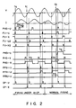
- Fig. 2 The timing of generation of various signals and their pulse widths in those gate circuits are illustrated in Fig. 2 by way of example.
- V represents a voltage waveform across each of the U-phase and X-phase valve
- I represents a current waveform flowing through each of the U-phase and X-phase valves.
- Flip-flop 1U is reset in the above way of either (a) or (b).
- the X-phase valve when flip-flop 1U is set by phase control signal PHS-X to produce the on period signal PHS1-X at a logic 1 and the on period signal PHS1-X is then ANDed with the forward voltage signal FV-X at a logic 1, a gate pulse GP-X is produced to fire the X-phase valve.
- time T3 is set to 2 to 3 ms or more, then flip-flop 1U and 1X which determine the on periods can be reset.
- timer T3 is set to 2 to 3 ms and time T4 is set to about 1 ms or less (1 to 0.7 ms).
- Gate circuits 100U and 100X of Fig. 1 handle many signals which are 1 ms or less in pulse width and thus need rather high speed operation.
- the high speed operation is easy to realize with such a circuit composed of discrete parts as shown in Fig. 1, but it is not so easy to realize with software control using an 8-bit microcomputer that is slow in operation.
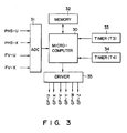
- Fig. 3 illustrates the main portion of an arrangement in which the gate circuit portion of Fig. 1 is replaced with such high-speed computer circuitry (circuits portions that handle phase control signals PHS-U and PHS-X and other signals are omitted).
- Phase control signals PHS-U and PHS-X and forward voltage signals FV-U and FV-X are input to a microcomputer 30 via A/D converter 31.
- microcomputer 30 Connected with microcomputer 30 are a memory 32 storing data and programs, a timer counter 33 which corresponds to timers 6U and 6X of Fig. 1 and thus provides a time delay of T3, a timer counter 34 which corresponds to timers 9U and 9X of Fig. 1 and thus provides a time delay of T4 and a driver 35 which feeds processing results as gate pulses GP-U and GP-X and so on to corresponding thyristor valves through optical fibers (not shown) or the like.
- the computer-controlled circuit of Fig. 3 operates as indicated by a flowchart of Fig. 4.
- step ST18 If the condition of step ST18 is met, then the count operation of timer counter 34 is initiated at the time of meeting of the condition (ST24).
- Fig. 1 is applied to a three-phase power system, but the present invention may be applied to a single-phase power system.
- the voltage detectors VDU and VDX of Fig. 1 may be arranged as shown in Fig. 10 of US Patent Application serial No. 216,538.
- a flip-flop (1) which produces a gate pulse, is reset during a period of time of T3 more than the turn-off time of thyristors in the valve so that all the thyristors in the valve can be turned off at the time of commutation and breakdown of thyristors due to partial commutation failure can be prevented.
Landscapes
- Engineering & Computer Science (AREA)
- Power Engineering (AREA)
- Control Of Electrical Variables (AREA)
- Supply And Distribution Of Alternating Current (AREA)
- Power Conversion In General (AREA)
- Rectifiers (AREA)
Applications Claiming Priority (2)
| Application Number | Priority Date | Filing Date | Title |
|---|---|---|---|
| JP63313234A JP2614293B2 (ja) | 1988-12-12 | 1988-12-12 | 無効電力補償装置 |
| JP313234/88 | 1988-12-12 |
Publications (3)
| Publication Number | Publication Date |
|---|---|
| EP0373601A2 true EP0373601A2 (de) | 1990-06-20 |
| EP0373601A3 EP0373601A3 (de) | 1991-08-21 |
| EP0373601B1 EP0373601B1 (de) | 1995-03-15 |
Family
ID=18038727
Family Applications (1)
| Application Number | Title | Priority Date | Filing Date |
|---|---|---|---|
| EP89122952A Expired - Lifetime EP0373601B1 (de) | 1988-12-12 | 1989-12-12 | Blindleistungskompensator mit verbesserter Gatterschaltung |
Country Status (4)
| Country | Link |
|---|---|
| EP (1) | EP0373601B1 (de) |
| JP (1) | JP2614293B2 (de) |
| CN (1) | CN1014946B (de) |
| CA (1) | CA2005308C (de) |
Cited By (3)
| Publication number | Priority date | Publication date | Assignee | Title |
|---|---|---|---|---|
| US5969509A (en) * | 1997-02-06 | 1999-10-19 | Asea Brown Boveri Ab | Method and a device for control of a capacitor device for a shunt-connected compensator unit |
| EP0858141A3 (de) * | 1997-02-06 | 1999-12-15 | Asea Brown Boveri Ab | Verfahren und Vorrichtung zur Steuerung einer kapazitiven Vorrichtung für eine Nebenschluss-Kompensatoreinheit |
| CN109525001A (zh) * | 2018-11-16 | 2019-03-26 | 国网河南省电力公司电力科学研究院 | 特高压分层接入下的换相失败预防协调控制方法及系统 |
Families Citing this family (1)
| Publication number | Priority date | Publication date | Assignee | Title |
|---|---|---|---|---|
| CN1321428C (zh) * | 2005-06-23 | 2007-06-13 | 华北电力大学(北京) | 一种高速低谐波的可控电抗器 |
Family Cites Families (6)
| Publication number | Priority date | Publication date | Assignee | Title |
|---|---|---|---|---|
| EP0128182B1 (de) * | 1982-12-11 | 1987-08-12 | Fairford Electronics Ltd. | Verfahren und anordnung zur automatischen sollwerteinstellung der verzögerten phase in einem leistungsfaktorregler eines induktionsmotors |
| JPS59110335A (ja) * | 1982-12-14 | 1984-06-26 | 富士電機株式会社 | サイリスタ式コンデンサ開閉装置 |
| FR2561463B1 (fr) * | 1984-03-13 | 1986-09-12 | Alsthom Cgee | Dispositif de generation d'impulsions de commande de thyristors pour l'alimentation d'une inductance de reglage de la puissance reactive d'un reseau electrique |
| US4755738A (en) * | 1986-09-11 | 1988-07-05 | Kabushiki Kaisha Toshiba | Reactive power compensation apparatus |
| JPS6416255A (en) * | 1987-07-10 | 1989-01-19 | Toshiba Corp | Gate signal generator |
| JP6311856B2 (ja) | 2013-10-31 | 2018-04-18 | パナソニックIpマネジメント株式会社 | 照明器具 |
-
1988
- 1988-12-12 JP JP63313234A patent/JP2614293B2/ja not_active Expired - Lifetime
-
1989
- 1989-12-12 EP EP89122952A patent/EP0373601B1/de not_active Expired - Lifetime
- 1989-12-12 CA CA002005308A patent/CA2005308C/en not_active Expired - Fee Related
- 1989-12-12 CN CN89109234A patent/CN1014946B/zh not_active Expired
Cited By (3)
| Publication number | Priority date | Publication date | Assignee | Title |
|---|---|---|---|---|
| US5969509A (en) * | 1997-02-06 | 1999-10-19 | Asea Brown Boveri Ab | Method and a device for control of a capacitor device for a shunt-connected compensator unit |
| EP0858141A3 (de) * | 1997-02-06 | 1999-12-15 | Asea Brown Boveri Ab | Verfahren und Vorrichtung zur Steuerung einer kapazitiven Vorrichtung für eine Nebenschluss-Kompensatoreinheit |
| CN109525001A (zh) * | 2018-11-16 | 2019-03-26 | 国网河南省电力公司电力科学研究院 | 特高压分层接入下的换相失败预防协调控制方法及系统 |
Also Published As
| Publication number | Publication date |
|---|---|
| CA2005308C (en) | 1995-05-23 |
| JPH02158814A (ja) | 1990-06-19 |
| EP0373601A3 (de) | 1991-08-21 |
| JP2614293B2 (ja) | 1997-05-28 |
| EP0373601B1 (de) | 1995-03-15 |
| CN1014946B (zh) | 1991-11-27 |
| CN1043591A (zh) | 1990-07-04 |
| CA2005308A1 (en) | 1990-06-12 |
Similar Documents
| Publication | Publication Date | Title |
|---|---|---|
| US4346434A (en) | Apparatus for controlling an electric motor | |
| Shanxu et al. | Parallel operation control technique of voltage source inverters in UPS | |
| AU668009B2 (en) | Auto-self test of AC motor system | |
| KR950013238B1 (ko) | 전력변환장치의 제어방법 및 장치 | |
| JPH02262832A (ja) | 半導体電力変換システム | |
| US4859884A (en) | Gate signal generator for thyristor valve | |
| US4580083A (en) | Chopper controller for a D.C. motor | |
| EP0373601A2 (de) | Blindleistungskompensator mit verbesserter Gatterschaltung | |
| US5170334A (en) | Bypass-pair control apparatus for thyristor bridge | |
| US4197575A (en) | Conduction through sensing and inverter protection system | |
| US4282570A (en) | Method and apparatus for controlling an output current of a controlled rectifier | |
| US4536835A (en) | Direct A.C. to A.C. converter controlled by a data processor | |
| US3560836A (en) | Means for protecting electric power converters from commutation failure | |
| JP3533515B2 (ja) | 直列補償装置とスイッチング素子制御装置 | |
| EP0314872A2 (de) | Digitaltorpulsgenerator für Cyclokonvertersteuerung | |
| CN1056966A (zh) | 监测电压脉冲宽度的电路和方法 | |
| JP3215263B2 (ja) | 交流電動機の駆動システム | |
| JPH08237952A (ja) | 交直変換装置の制御装置 | |
| JPS6148015A (ja) | デイジタル位相制御装置 | |
| SU1760596A1 (ru) | Устройство дл управлени и защиты резонансного инвертора | |
| JPH07106034B2 (ja) | 交直変換装置の制御方式 | |
| VanderLaan et al. | DIII-D power supply fault system | |
| Seki et al. | New GTO uninterruptible power supplies with self-diagnosis functions | |
| JPS6251076B2 (de) | ||
| JPH0345991B2 (de) |
Legal Events
| Date | Code | Title | Description |
|---|---|---|---|
| PUAI | Public reference made under article 153(3) epc to a published international application that has entered the european phase |
Free format text: ORIGINAL CODE: 0009012 |
|
| 17P | Request for examination filed |
Effective date: 19900109 |
|
| AK | Designated contracting states |
Kind code of ref document: A2 Designated state(s): CH DE GB LI SE |
|
| PUAL | Search report despatched |
Free format text: ORIGINAL CODE: 0009013 |
|
| AK | Designated contracting states |
Kind code of ref document: A3 Designated state(s): CH DE GB LI SE |
|
| 17Q | First examination report despatched |
Effective date: 19930215 |
|
| RBV | Designated contracting states (corrected) |
Designated state(s): GB |
|
| REG | Reference to a national code |
Ref country code: DE Ref legal event code: 8566 |
|
| GRAA | (expected) grant |
Free format text: ORIGINAL CODE: 0009210 |
|
| AK | Designated contracting states |
Kind code of ref document: B1 Designated state(s): GB |
|
| PLBE | No opposition filed within time limit |
Free format text: ORIGINAL CODE: 0009261 |
|
| STAA | Information on the status of an ep patent application or granted ep patent |
Free format text: STATUS: NO OPPOSITION FILED WITHIN TIME LIMIT |
|
| 26N | No opposition filed | ||
| REG | Reference to a national code |
Ref country code: GB Ref legal event code: 746 Effective date: 19980929 |
|
| PGFP | Annual fee paid to national office [announced via postgrant information from national office to epo] |
Ref country code: GB Payment date: 19981218 Year of fee payment: 10 |
|
| PG25 | Lapsed in a contracting state [announced via postgrant information from national office to epo] |
Ref country code: GB Free format text: LAPSE BECAUSE OF NON-PAYMENT OF DUE FEES Effective date: 19991212 |
|
| GBPC | Gb: european patent ceased through non-payment of renewal fee |
Effective date: 19991212 |