EP0373672A2 - Halbleiterspeicherschaltung mit einer verbesserten Wiederherstellungssteuerschaltung - Google Patents
Halbleiterspeicherschaltung mit einer verbesserten Wiederherstellungssteuerschaltung Download PDFInfo
- Publication number
- EP0373672A2 EP0373672A2 EP89123262A EP89123262A EP0373672A2 EP 0373672 A2 EP0373672 A2 EP 0373672A2 EP 89123262 A EP89123262 A EP 89123262A EP 89123262 A EP89123262 A EP 89123262A EP 0373672 A2 EP0373672 A2 EP 0373672A2
- Authority
- EP
- European Patent Office
- Prior art keywords
- bit lines
- memory
- memory cells
- coupled
- circuit
- Prior art date
- Legal status (The legal status is an assumption and is not a legal conclusion. Google has not performed a legal analysis and makes no representation as to the accuracy of the status listed.)
- Granted
Links
Images




Classifications
-
- G—PHYSICS
- G11—INFORMATION STORAGE
- G11C—STATIC STORES
- G11C11/00—Digital stores characterised by the use of particular electric or magnetic storage elements; Storage elements therefor
- G11C11/21—Digital stores characterised by the use of particular electric or magnetic storage elements; Storage elements therefor using electric elements
- G11C11/34—Digital stores characterised by the use of particular electric or magnetic storage elements; Storage elements therefor using electric elements using semiconductor devices
- G11C11/40—Digital stores characterised by the use of particular electric or magnetic storage elements; Storage elements therefor using electric elements using semiconductor devices using transistors
- G11C11/401—Digital stores characterised by the use of particular electric or magnetic storage elements; Storage elements therefor using electric elements using semiconductor devices using transistors forming cells needing refreshing or charge regeneration, i.e. dynamic cells
- G11C11/4063—Auxiliary circuits, e.g. for addressing, decoding, driving, writing, sensing or timing
- G11C11/407—Auxiliary circuits, e.g. for addressing, decoding, driving, writing, sensing or timing for memory cells of the field-effect type
- G11C11/409—Read-write [R-W] circuits
- G11C11/4094—Bit-line management or control circuits
-
- G—PHYSICS
- G11—INFORMATION STORAGE
- G11C—STATIC STORES
- G11C11/00—Digital stores characterised by the use of particular electric or magnetic storage elements; Storage elements therefor
- G11C11/21—Digital stores characterised by the use of particular electric or magnetic storage elements; Storage elements therefor using electric elements
- G11C11/34—Digital stores characterised by the use of particular electric or magnetic storage elements; Storage elements therefor using electric elements using semiconductor devices
- G11C11/40—Digital stores characterised by the use of particular electric or magnetic storage elements; Storage elements therefor using electric elements using semiconductor devices using transistors
- G11C11/401—Digital stores characterised by the use of particular electric or magnetic storage elements; Storage elements therefor using electric elements using semiconductor devices using transistors forming cells needing refreshing or charge regeneration, i.e. dynamic cells
- G11C11/4063—Auxiliary circuits, e.g. for addressing, decoding, driving, writing, sensing or timing
- G11C11/407—Auxiliary circuits, e.g. for addressing, decoding, driving, writing, sensing or timing for memory cells of the field-effect type
- G11C11/408—Address circuits
- G11C11/4085—Word line control circuits, e.g. word line drivers, - boosters, - pull-up, - pull-down, - precharge
-
- G—PHYSICS
- G11—INFORMATION STORAGE
- G11C—STATIC STORES
- G11C11/00—Digital stores characterised by the use of particular electric or magnetic storage elements; Storage elements therefor
- G11C11/21—Digital stores characterised by the use of particular electric or magnetic storage elements; Storage elements therefor using electric elements
- G11C11/34—Digital stores characterised by the use of particular electric or magnetic storage elements; Storage elements therefor using electric elements using semiconductor devices
- G11C11/40—Digital stores characterised by the use of particular electric or magnetic storage elements; Storage elements therefor using electric elements using semiconductor devices using transistors
- G11C11/401—Digital stores characterised by the use of particular electric or magnetic storage elements; Storage elements therefor using electric elements using semiconductor devices using transistors forming cells needing refreshing or charge regeneration, i.e. dynamic cells
- G11C11/4063—Auxiliary circuits, e.g. for addressing, decoding, driving, writing, sensing or timing
- G11C11/407—Auxiliary circuits, e.g. for addressing, decoding, driving, writing, sensing or timing for memory cells of the field-effect type
- G11C11/409—Read-write [R-W] circuits
- G11C11/4097—Bit-line organisation, e.g. bit-line layout, folded bit lines
Definitions
- the present invention relates to a semiconductor memory circuit and, more particularly to a dynamic type random access memory (DRAM) fabricated on a semiconductor substrate.
- DRAM dynamic type random access memory
- Dynamic memory circuits have been widely utilized as large capacity semiconductor memories in various fields.
- the dynamic memory circuit is generally constructed in such a manner that one-transistor type memory cells are arranged in a matrix form of rows and columns together with word lines and bit lines arranged in rows and columns, respectively.
- the number of memory cells connected to one bit line increases as the memory capacity increases. Consequently, a stray capacitance of each bit line increases to cause various problems.
- the bit lines need to be charged or discharged to a power supply potential Vcc or a ground potential Vss.
- the increase in the stray capacitances of the bit lines cause an increase in the time required for charging and discharging. If the respective pairs of bit lines are not sufficiently amplified, that is, if charging or discharging is not sufficiently effected, it is impossible to enable a column selection circuit so as to connect the selected pair of bit lines to a pair of common data lines.
- the floating of the ground potential during the active period causes a noise due to operations of peripheral circuits such as an output circuit, the column selection circuit, and a potential of the non-selected word lines undesirably exceeds a threshold voltage of memory cell transistors or more, storage capacitors of the non-selected memory cells are erroneously connected to the bit lines, resulting in destruction of the stored data.
- the dynamic memory comprises means for receiving an external control signal having a first level which sets the memory in an active state and a second level which sets the memory in a reset state and dynamic memory cells which require restoring read-out data therein and, is featured in that read-out of data from a memory cell or cells is performed in the active state and restoring of data to the memory cell or cells is conducted in the reset state.
- a time required for the restoring of data to the memory cells is removed in the active state can be shortened and a current amount required in the active state is reduced.
- bit lines are not charged or discharged in the active state but left near a precharged level with small signal difference, memory cell transistors of the memory cells coupled to the non-selected word lines are never turned conductive even when the potential of the non-selected word lines float in levels. Thus, destruction of data stored in the non-selected memory cells can be effectively prevented.
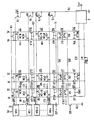
- the memory comprises a plurality of one-transistor type memory cells MC11 - MC nN each having a memory cell transistor Q M and a storage capacitor C M connected between the transistor Q M and a fixed potential V f , word lines WL1 - WL n arranged in rows, a plurality of bit line pairs D1, D1 - D N , D N arranged in columns, CMOS type sense amplifiers SA1 - SA N provided for the bit line pairs D1, D1 - D N , D N , respectively, a pair of common data lines I/O, I/O , a plurality of pairs of column selection transistors QY1, QY1′ - QY N , QY N ′ connected between the bit line pairs and the pair of common data lines, respectively, a row decoder 20 having decoding units WD1 - WD n for selecting the word lines WL1 - WL n , and an output circuit 11.
- the row decoder 20 operatively selects one of the word lines WL1 - WL n in accordance with row address signals ADR in response to a timing signal RA.
- Each of the sense amplifiers SA1 - SA N includes P-channel MOS transistors QPl, QP2 and N-channel MOS transistors Q1, Q2 and is connected to a first activation line SAP and a second activation signal SAN .
- the activation line SAP is connected to a p-channel MOS transistor QP3 controlled by a control signal SEP and the activation line SAN is coupled to an N-channel MOS transistor Q10 controlled by a control signal SEN.
- the pairs of column selection transistors QY1, QY1′ - QY N , QY N ′ are controlled by column decoder signals YSW1 - YSW N generated by a column decoder (not shown) in a known way.
- the row decoder 20 also generates clamp signals ⁇ w1 - ⁇ wn which are opposite to those outputs for the word lines WL1 - WL n , respectively. For example, when the word line WL1 is selected (high level), the signals ⁇ w2 - ⁇ wn are high in level with ⁇ w1 at a low level. Clamp transistors of N-channel type QL1 - QL n are connected between the word lines WL1 - WL n and a ground wiring GL1 which is extending through the output circuit 11 and connected to the output circuit 11. The clamp transistors QL1 - QL n receive the clamp signals ⁇ w1 - ⁇ wn , respectively. While the source of the transistor Q10 is connected to a separate ground wiring GL2.
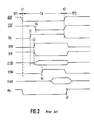
- the bit lines D1, D1 to D N , D N have been maintained at, for example, an intermediate potential (1/2 Vcc) of a power supply potential Vcc and a ground potential Vss.
- the row address strobe signal RAS becomes an active, low level at t1
- the active period T A is initiated and one word line driving circuit, for example, WDi, is selected among the word line driving circuits WD1 to WD n on the basis of row address signals ADR given externally in response to RA which is an internal signal formed front RAS at t2, so that one selected word line e.g. WLi rises in potential.
- the memory cell transistors Q M of the memory cells MCil to MCiN turn ON, so that the potentials of one bit lines of the bit line pairs D1, D1 to D N , D N change in the range of from about 100 mV to 200 mV in accordance with charges stored in the respective storage capacitors C M .
- the potentials of the other bit lines remain at the initial value, that is, the potential of 1/2 Vcc. Accordingly, the signals representative of the potential differences are input to the sense amplifiers SA1 to SA N , respectively.
- the sense amplifier enabling signal SEN rises and SEP falls at t3
- the sense amplifiers SA1 to SA N are activated to amplify the very small difference signals input to the sense amplifiers.
- the bit line D1 lowers to the ground potential, while the bit line D1 rises to the power supply potential Vcc (in the case where the memory cell MCil has "0" information (L) stored therein).
- the information in the capacitor C M of the memory cell MCil is destroyed through the exchange of charges with the bit line D1 when the word line WLi rises to read out information to the bit line D1. Therefore, the above-described sense amplifier operation serves not only to amplify the very small signals on the bit lines D1 and D1 but also to rewrite (i.e., refresh) the destroyed information to the memory cell by reading out the signals to the bit lines.
- the column decoder signal YSW which is an internal signal generated from a column address strobe CAS on the basis of column address signals (not shown) given to an external address terminal in response to the fall of the column address strobe CAS , rises, so that, for example, YSW1 is selected and rises at t5.
- the data from the bit line pair D1 and D1 is transferred to the common data line pair I/O and I/O .
- the transferred data is amplified by the output circuit 11 and output to the outside from the output terminal Dout.
- the active period T A is terminated at t6 and the reset signal ⁇ p rises at t7.
- bit line pairs D1, D1 to D N , D N are not sufficiently amplified, that is, if charging or discharging is not sufficiently effected, it is impossible to enable YSW so as to connect bit lines to the common data lines I/O and I/O . This is because, when the common data lines are connected to bit lines, the charges on the common data lines may flow into the bit lines to destroy the information. In consequence, the time at which the data is output from the output terminal Dout is delayed, which results in the performance being deteriorated.
- the increase in the bit line stray capacitances C31 invites an increase in the charging and discharging current, thus causing problems, for example, floating of the ground potential, a lowering in the power supply potential, and generation of noise between the bit lines.
- either the bit line D1 or D1 is discharged to the ground potential during the active period T A when the row address strobe signal RAS is at the low potential. Therefore, if a noise is generated in the internal grounding wiring GL1 due to the activation of the output circuit 11 during this period, the potentials of the wiring GL1 and the non-selected word lines, for example, WLi+1, undesirably rises from the ground potential to a potential near the threshold voltage of the memory cell transistors Q M , while the bit line D1 already becomes the ground potential, and if the memory cell MCi+11 has information "1" (H) stored therein, the sub-threshold current of the MOS transistor in the memory cell MCi+11 causes the charge in the capacitor of the memory cell MCi+11 to flow out to the bit line D1, thus causing destruction of the stored information.
- the sub-threshold current of the MOS transistor in the memory cell MCi+11 causes the charge in the capacitor of the memory cell MCi+11
- the memory of this embodiment is featured as follows. Namely, a plurality of pairs of transfer gate (N-channel) transistors QT1, QT1 - QT N , QT N are inserted between the pairs of bit lines D1, D1 - D N , D N and a plurality of pairs of sense nodes D1′, D 1′ - D N ′, D N ′ of the sense amplifiers SA1 - SA N , respectively.
- the purpose of provision of the transfer gates Q T1 to Q TN is to cut off the bit line stray capacitances C11 from the stray capacitances C11′ of the sense nodes D1′ to D N ′ when the sense amplifiers are activated, thereby increasing the operating speed of the sense amplifiers.
- a timing signal generator 30 receives the row address strobe signal RAS and generates timing signals RA′, SEP′, SEN′, TG and ⁇ p ′.
- a column decoder 40 receives column address signals ADC and generates the column decoder signals YSW1 - YSW N under control of CAS and RA′.
- a restoring or rewriting operation is conducted during a reset period when RAS is made inactive under control of RA′, SEP′, SEN′, TG and ⁇ p ′ generated by the timing signal generator 30.
- a reset period TP1 Prior to a time point t1, a reset period TP1 has been set and the pairs of bit lines D1, D1 - D N , D N and the sense nodes D1′, D1′ - D N ′, D N ′ have been precharged to a precharge potential (1/2 Vcc level).
- the row address strobe signal RAS becomes active (low level) to introduce the active period the row address signals ADR are taken in, and on the basis of this address signals one word line driving unit, for example, WDi, is selected from among the word line driving circuits WD1 to WD n .
- the potential of the selected word line WLi rises and consequently information stored in the memory cells MCi1 to MCi N connected to thr selected word line WLi appear as very small signals on the bit line pairs D1, D1 to D N , D N , respectively. Since at this time the transfer gate control signal TG is at the high potential, the signals on the bit line pairs D1, D1 to D N , D N are also transferred to the sense nodes D1′, D1′ to D N ′, D N ′ respectively.
- the control signal TG is lowered to turn OFF the transfer gates Q T1 to Q TN , thereby cuttint off the bit lines D1 to D N from the sense nodes D1′ to D N ′ .
- the sense amplifier enabling signals SEN′ and SEP′ are raised and lowered, respectively, to activate the sense amplifiers SA1 to SA N . Since the sense nodes D1′ to D N ′ have relatively small stray capacitances C11′, as described above, they are amplified at high speed. As a result, for example, one sense node D1′ reaches the power supply potential Vcc, while the other sense node D1′ reaches the ground potential, rapidly.
- the column selection transistors for example, Q Y1 and Q Y1 , selected after the column address strobe signal CAS becomes active at t5 on the basis of the externally applied column address information ADC, are driven to turn ON in response to the rise of the internal signal YSW at t6 generated on the basis of CAS , so that the data from the sense nodes D1′ to D1′ is transferred to the common data line pair I/O and I/O and output from the output terminal Dout via the output circuit 11.
- the transfer gate control signal TG remains at the low potential and therefore the bit lines D1 to D N are not charged nor discharged but maintained near the middle potential.
- the internal signal YSW is first lowered to turn OFF the column selections transistors Q Y1 and Q Y1 , thereby cutting off the sense nodes D1′ and D1′ from the common data line pair I/O and I/O .
- the transfer gate control signal TG is raised to start charging and discharging of the bit lines D1 to D N by the sense amplifiers SA1 to SA N which have been left activated.
- the word line driving signal RA′ is lowered to lower the selected word line WLi.
- the refreshing of the memory cells MCil to MCiN is completed.
- the sense amplifier enabling signals SEN′ and SEP′ are reset at t10 and the bit line sense nodes are also reset, thus completing the operation.
- the arrangement in which N-type MOS transistors are employed as switching elements and CMOS type sense amplifiers are used has been described.
- various changes and modifications may be made to matters of design, for example, the selection of the above-mentioned parts and the set values for the initial and finally reached potentials, of the bit lines according to circumstances.
- the subject matter of the present application resides in that after the information stored in a memory cell has been transferred to the sense nodes during the active period, the sense nodes and the bit lines are left cut off from each other so as not to carry out charging or discharging of the bit lines.
- the restoring data to the memory cells is conducted during the reset period after the active period T A , and therefore, the effective length of the active period is shortened as viewed from the outside of the memory, thus, data rate in the access operation can be improved.
- the memory cell transistors Q M of the non-selected memory cells are kept non-conductive by performing the restore operation in the reset period, destruction of stored data can be effectively prevented.
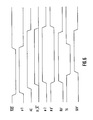
- Timing signal generator 30 in Fig. 3 An example of the timing signal generator 30 in Fig. 3 will be explained with reference to Figs. 5 and 6.
- the timing signal generator 30 includes delay circuits D1 to D7, inverting delay circuits ID1 and ID2, inverter circuits IV1 to IV10, a dummy row address buffer 51, NAND gates 52, 54, 55, 56 and 57, a NOR gate 53, and a series circuit of P-channel MOS transistor QP5 and N-channel MOS transistors Q51, Q52.
- An internal signal ⁇ 1 is generated from RAS through the delay circuit D1 and the inverter IV2 and has the substantially opposite phase to RAS .
- a control signal AE which is used to enable row address buffers (not shown in Fig. 3) is generated from the delay circuit D3.
- the dummy row address buffer 51 receives one of row address signals Ai and generates its true and complementary buffered signals Xi, Xi when enabled by AE.
- the signals Xi, Xi are applied to the NOR gate 53, the inverter IV3 and the delay circuit D4 in cascade and, an internal signal ⁇ 2 is generated when the states of Xi and Xi are established.
- the internal signals ⁇ 1 and ⁇ 2 are applied to the NAND gate 54 for generation of RA′ and TG, as illustrated.
- Fig. 7 shows the arrangement of a second embodiment of the present invention. This arrangement differs from the arrangement shown in Fig. 3 in that bit lines are divided into two groups d 1a , d 1a - d Na , d Na and d 1b , d 1b - d Nb , d Nb , which are separated from each other through second transfer gates Q T1 ′, Q T1 ′ to Q TN ′, Q TN ′ .
- the operation is substantially the same as that of the foregoing first embodiment except for the following. Namely, at the time when the transfer gate control signal TG is lowered at t3 in the first embodiment in the active period T A , the first and second transfer gate control signals TG and TG2 of the second embodiment are lowered simultaneously or successively in the mentioned order and thereafter both maintained at the low potential during the active periot T A to maintain the bit lines d 1a , d 1a to d Na , d Na and d 1b , d 1b to d Nb , d Nb near the middle potential.
- the control signal TG is raised and the control signal TG2 is raised with a little delay at t2.
- the feature of the second embodiment resides in that the bit lines are divided and charged or discharged in a time division manner at the time of refreshing. Thus, it is possible to reduce the generation of noise.
- the sense nodes and the bit lines are cut off from each other so as to maintain the bit line potential near the middle potential between the power supply potential and the ground potential, thereby making it possible to prevent destruction of the information stored in non-selected memory cells due to floating or sinking of the non-selected word lines caused by the ground potential line noise in the chip that is attendant on the operations of other circuit blocks on the same chip, for example, the CAS circuit block, column address buffer and column address decoder circuit, during the active period.
Landscapes
- Engineering & Computer Science (AREA)
- Microelectronics & Electronic Packaging (AREA)
- Computer Hardware Design (AREA)
- Dram (AREA)
- Static Random-Access Memory (AREA)
Applications Claiming Priority (2)
| Application Number | Priority Date | Filing Date | Title |
|---|---|---|---|
| JP63317827A JPH07105140B2 (ja) | 1988-12-16 | 1988-12-16 | 半導体メモリ |
| JP317827/88 | 1988-12-16 |
Publications (3)
| Publication Number | Publication Date |
|---|---|
| EP0373672A2 true EP0373672A2 (de) | 1990-06-20 |
| EP0373672A3 EP0373672A3 (de) | 1991-04-17 |
| EP0373672B1 EP0373672B1 (de) | 1995-03-01 |
Family
ID=18092496
Family Applications (1)
| Application Number | Title | Priority Date | Filing Date |
|---|---|---|---|
| EP89123262A Expired - Lifetime EP0373672B1 (de) | 1988-12-16 | 1989-12-15 | Halbleiterspeicherschaltung mit einer verbesserten Wiederherstellungssteuerschaltung |
Country Status (4)
| Country | Link |
|---|---|
| US (1) | US5148400A (de) |
| EP (1) | EP0373672B1 (de) |
| JP (1) | JPH07105140B2 (de) |
| DE (1) | DE68921440T2 (de) |
Cited By (8)
| Publication number | Priority date | Publication date | Assignee | Title |
|---|---|---|---|---|
| EP0484920A3 (en) * | 1990-11-09 | 1993-07-21 | Nec Corporation | Random access memory device having transfer gate unit for blocking flush write data buffer unit from parasitic capacitance coupled with bit line pairs of memory cells |
| EP0485239A3 (en) * | 1990-11-09 | 1993-08-11 | Nec Corporation | Semiconductor memory device |
| EP0474238A3 (en) * | 1990-09-05 | 1994-09-28 | Nippon Electric Co | Semiconductor memory circuit |
| EP0561271A3 (de) * | 1992-03-17 | 1995-07-26 | Hitachi Ltd | |
| US5687345A (en) * | 1992-03-17 | 1997-11-11 | Hitachi, Ltd. | Microcomputer having CPU and built-in flash memory that is rewritable under control of the CPU analyzing a command supplied from an external device |
| US6414878B2 (en) | 1992-03-17 | 2002-07-02 | Hitachi, Ltd. | Data line disturbance free memory block divided flash memory and microcomputer having flash memory therein |
| US7057937B1 (en) | 1992-03-17 | 2006-06-06 | Renesas Technology Corp. | Data processing apparatus having a flash memory built-in which is rewritable by use of external device |
| US7508691B2 (en) | 2004-10-27 | 2009-03-24 | Infineon Technologies Ag | Memory arrangement with low power consumption |
Families Citing this family (5)
| Publication number | Priority date | Publication date | Assignee | Title |
|---|---|---|---|---|
| US5241503A (en) * | 1991-02-25 | 1993-08-31 | Motorola, Inc. | Dynamic random access memory with improved page-mode performance and method therefor having isolator between memory cells and sense amplifiers |
| US5311477A (en) * | 1991-07-17 | 1994-05-10 | Sgs-Thomson Microelectronics, Inc. | Integrated circuit memory device having flash clear |
| KR960000619B1 (ko) * | 1991-12-27 | 1996-01-10 | 후지쓰 가부시끼가이샤 | 일괄소거형의 불휘발성 반도체 기억장치 및 그의 구동제어회로 |
| JP2973668B2 (ja) * | 1991-12-27 | 1999-11-08 | 日本電気株式会社 | 高速ダイナミックランダムアクセスメモリ装置 |
| CA2117967A1 (en) * | 1993-10-27 | 1995-04-28 | Thomas W. Sander | Tissue repair device and apparatus and method for fabricating same |
Family Cites Families (7)
| Publication number | Priority date | Publication date | Assignee | Title |
|---|---|---|---|---|
| US3737879A (en) * | 1972-01-05 | 1973-06-05 | Mos Technology Inc | Self-refreshing memory |
| US3810124A (en) * | 1972-06-30 | 1974-05-07 | Ibm | Memory accessing system |
| JPS6012718B2 (ja) * | 1980-03-28 | 1985-04-03 | 富士通株式会社 | 半導体ダイナミックメモリ |
| KR900005667B1 (ko) * | 1984-11-20 | 1990-08-03 | 후지쓰 가부시끼가이샤 | 반도체 기억장치 |
| US4679172A (en) * | 1985-05-28 | 1987-07-07 | American Telephone And Telegraph Company, At&T Bell Laboratories | Dynamic memory with increased data retention time |
| JPS62202397A (ja) * | 1986-02-28 | 1987-09-07 | Fujitsu Ltd | 半導体記憶装置 |
| JPH07105137B2 (ja) * | 1987-11-17 | 1995-11-13 | 日本電気株式会社 | 半導体メモリ |
-
1988
- 1988-12-16 JP JP63317827A patent/JPH07105140B2/ja not_active Expired - Lifetime
-
1989
- 1989-12-15 EP EP89123262A patent/EP0373672B1/de not_active Expired - Lifetime
- 1989-12-15 DE DE68921440T patent/DE68921440T2/de not_active Expired - Fee Related
-
1991
- 1991-01-23 US US07/644,865 patent/US5148400A/en not_active Expired - Lifetime
Cited By (26)
| Publication number | Priority date | Publication date | Assignee | Title |
|---|---|---|---|---|
| EP0474238A3 (en) * | 1990-09-05 | 1994-09-28 | Nippon Electric Co | Semiconductor memory circuit |
| EP0484920A3 (en) * | 1990-11-09 | 1993-07-21 | Nec Corporation | Random access memory device having transfer gate unit for blocking flush write data buffer unit from parasitic capacitance coupled with bit line pairs of memory cells |
| EP0485239A3 (en) * | 1990-11-09 | 1993-08-11 | Nec Corporation | Semiconductor memory device |
| US6181598B1 (en) | 1992-03-17 | 2001-01-30 | Hitachi, Ltd. | Data line disturbance free memory block divided flash memory and microcomputer having flash memory |
| US6400609B1 (en) | 1992-03-17 | 2002-06-04 | Hitachi, Ltd. | Data line disturbance free memory block divided flash memory and microcomputer having flash memory therein |
| US5687345A (en) * | 1992-03-17 | 1997-11-11 | Hitachi, Ltd. | Microcomputer having CPU and built-in flash memory that is rewritable under control of the CPU analyzing a command supplied from an external device |
| US5768194A (en) * | 1992-03-17 | 1998-06-16 | Hitachi, Ltd. | Data line disturbance free memory block divided flash memory and microcomputer having flash memory therein |
| US5844843A (en) * | 1992-03-17 | 1998-12-01 | Hitachi, Ltd. | Single chip data processing apparatus having a flash memory which is rewritable under the control of built-in CPU in the external write mode |
| US6026020A (en) * | 1992-03-17 | 2000-02-15 | Hitachi, Ltd. | Data line disturbance free memory block divided flash memory and microcomputer having flash memory therein |
| US6064593A (en) * | 1992-03-17 | 2000-05-16 | Hitachi, Ltd. | Semiconductor integrated circuit device having an electrically erasable and programmable nonvolatile memory and a built-in processing unit |
| US6130836A (en) * | 1992-03-17 | 2000-10-10 | Hitachi, Ltd. | Semiconductor IC device having a control register for designating memory blocks for erasure |
| US6166953A (en) * | 1992-03-17 | 2000-12-26 | Hitachi, Ltd. | Data line disturbance free memory block divided flash memory and microcomputer having flash memory therein |
| EP0561271A3 (de) * | 1992-03-17 | 1995-07-26 | Hitachi Ltd | |
| US6335879B1 (en) | 1992-03-17 | 2002-01-01 | Hitachi, Ltd. | Method of erasing and programming a flash memory in a single-chip microcomputer having a processing unit and memory |
| US5581503A (en) * | 1992-03-17 | 1996-12-03 | Hitachi, Ltd. | Data line disturbance free memory block divided flash memory and microcomputer having flash memory therein |
| US6414878B2 (en) | 1992-03-17 | 2002-07-02 | Hitachi, Ltd. | Data line disturbance free memory block divided flash memory and microcomputer having flash memory therein |
| US6493271B2 (en) | 1992-03-17 | 2002-12-10 | Hitachi, Ltd. | Data line disturbance free memory block divided flash memory and microcomputer having flash memory therein |
| US6690603B2 (en) | 1992-03-17 | 2004-02-10 | Hitachi, Ltd. | Microcomputer including a flash memory that is two-way programmable |
| US6804152B2 (en) | 1992-03-17 | 2004-10-12 | Renesas Technology Corp. | Method for manufacturing a printed board on which a semiconductor device having two modes is mounted |
| US6999350B2 (en) | 1992-03-17 | 2006-02-14 | Renesas Technology Corp. | Data line disturbance free memory block divided flash memory and microcomputer having flash memory therein |
| US7057937B1 (en) | 1992-03-17 | 2006-06-06 | Renesas Technology Corp. | Data processing apparatus having a flash memory built-in which is rewritable by use of external device |
| US7184321B2 (en) | 1992-03-17 | 2007-02-27 | Hitachi Ulsi Systems Co., Ltd. | Data line disturbance free memory block divided flash memory and microcomputer having flash memory therein |
| US7295476B2 (en) | 1992-03-17 | 2007-11-13 | Renesas Technology Corp. | Data line disturbance free memory block divided flash memory and microcomputer having flash memory therein |
| US7505329B2 (en) | 1992-03-17 | 2009-03-17 | Renesas Technology Corp. | Data line disturbance free memory block divided flash memory and microcomputer having flash memory therein |
| US7965563B2 (en) | 1992-03-17 | 2011-06-21 | Renesas Technology Corp. | Data line disturbance free memory block divided flash memory and microcomputer having flash memory therein |
| US7508691B2 (en) | 2004-10-27 | 2009-03-24 | Infineon Technologies Ag | Memory arrangement with low power consumption |
Also Published As
| Publication number | Publication date |
|---|---|
| DE68921440D1 (de) | 1995-04-06 |
| EP0373672B1 (de) | 1995-03-01 |
| EP0373672A3 (de) | 1991-04-17 |
| US5148400A (en) | 1992-09-15 |
| DE68921440T2 (de) | 1995-11-09 |
| JPH02162594A (ja) | 1990-06-22 |
| JPH07105140B2 (ja) | 1995-11-13 |
Similar Documents
| Publication | Publication Date | Title |
|---|---|---|
| US4161040A (en) | Data-in amplifier for an MISFET memory device having a clamped output except during the write operation | |
| US4503522A (en) | Dynamic type semiconductor monolithic memory | |
| US5274598A (en) | Semiconductor memory having improved sensing arrangement | |
| US4943952A (en) | Semiconductor memory circuit with improved bit lane precharge circuit | |
| US4222112A (en) | Dynamic RAM organization for reducing peak current | |
| EP0316902B1 (de) | Halbleiterspeicherschaltung mit einem verbesserten Rückschreibschema | |
| US4397003A (en) | Dynamic random access memory | |
| US5255235A (en) | Dynamic random access memory with dummy word lines connected to bit line potential adjusting capacitors | |
| US5184324A (en) | Dynamic semiconductor multi-value memory device | |
| US4608670A (en) | CMOS sense amplifier with N-channel sensing | |
| EP0373672B1 (de) | Halbleiterspeicherschaltung mit einer verbesserten Wiederherstellungssteuerschaltung | |
| EP0124868B1 (de) | Halbleiterspeicher | |
| US5323345A (en) | Semiconductor memory device having read/write circuitry | |
| US4982367A (en) | Dynamic random access memory with well-balanced read-out voltage on bit line pair and operating method therefor | |
| US5014246A (en) | Semiconductor memory device having shared sense amplifier and operating method thereof | |
| JP2939027B2 (ja) | 半導体記憶装置 | |
| US4578781A (en) | MIS transistor circuit | |
| US20020027799A1 (en) | Ferroelectric memory device | |
| US4602355A (en) | Memory circuit with noise preventing means for word lines | |
| US5930196A (en) | Multi-bank memory device with compensation for line loading | |
| US4477886A (en) | Sense/restore circuit for dynamic random access memory | |
| US4281399A (en) | Semiconductor memory device | |
| US4409672A (en) | Dynamic semiconductor memory device | |
| US4878201A (en) | Semiconductor memory device having an improved timing signal generator for the column selection circuit | |
| US5777934A (en) | Semiconductor memory device with variable plate voltage generator |
Legal Events
| Date | Code | Title | Description |
|---|---|---|---|
| PUAI | Public reference made under article 153(3) epc to a published international application that has entered the european phase |
Free format text: ORIGINAL CODE: 0009012 |
|
| 17P | Request for examination filed |
Effective date: 19891215 |
|
| AK | Designated contracting states |
Kind code of ref document: A2 Designated state(s): DE FR GB |
|
| PUAL | Search report despatched |
Free format text: ORIGINAL CODE: 0009013 |
|
| AK | Designated contracting states |
Kind code of ref document: A3 Designated state(s): DE FR GB |
|
| 17Q | First examination report despatched |
Effective date: 19930729 |
|
| GRAA | (expected) grant |
Free format text: ORIGINAL CODE: 0009210 |
|
| AK | Designated contracting states |
Kind code of ref document: B1 Designated state(s): DE FR GB |
|
| REF | Corresponds to: |
Ref document number: 68921440 Country of ref document: DE Date of ref document: 19950406 |
|
| ET | Fr: translation filed | ||
| PLBE | No opposition filed within time limit |
Free format text: ORIGINAL CODE: 0009261 |
|
| STAA | Information on the status of an ep patent application or granted ep patent |
Free format text: STATUS: NO OPPOSITION FILED WITHIN TIME LIMIT |
|
| 26N | No opposition filed | ||
| PGFP | Annual fee paid to national office [announced via postgrant information from national office to epo] |
Ref country code: DE Payment date: 20001211 Year of fee payment: 12 |
|
| PGFP | Annual fee paid to national office [announced via postgrant information from national office to epo] |
Ref country code: FR Payment date: 20001212 Year of fee payment: 12 |
|
| PGFP | Annual fee paid to national office [announced via postgrant information from national office to epo] |
Ref country code: GB Payment date: 20001213 Year of fee payment: 12 |
|
| PG25 | Lapsed in a contracting state [announced via postgrant information from national office to epo] |
Ref country code: GB Free format text: LAPSE BECAUSE OF NON-PAYMENT OF DUE FEES Effective date: 20011215 |
|
| REG | Reference to a national code |
Ref country code: GB Ref legal event code: IF02 |
|
| PG25 | Lapsed in a contracting state [announced via postgrant information from national office to epo] |
Ref country code: DE Free format text: LAPSE BECAUSE OF NON-PAYMENT OF DUE FEES Effective date: 20020702 |
|
| GBPC | Gb: european patent ceased through non-payment of renewal fee |
Effective date: 20011215 |
|
| PG25 | Lapsed in a contracting state [announced via postgrant information from national office to epo] |
Ref country code: FR Free format text: LAPSE BECAUSE OF NON-PAYMENT OF DUE FEES Effective date: 20020830 |
|
| REG | Reference to a national code |
Ref country code: FR Ref legal event code: ST |