EP0373773A1 - Séparation de cartes de circuit électriques d'unités d'alimentation - Google Patents
Séparation de cartes de circuit électriques d'unités d'alimentation Download PDFInfo
- Publication number
- EP0373773A1 EP0373773A1 EP89311923A EP89311923A EP0373773A1 EP 0373773 A1 EP0373773 A1 EP 0373773A1 EP 89311923 A EP89311923 A EP 89311923A EP 89311923 A EP89311923 A EP 89311923A EP 0373773 A1 EP0373773 A1 EP 0373773A1
- Authority
- EP
- European Patent Office
- Prior art keywords
- board
- state
- clock signal
- enable
- disable means
- Prior art date
- Legal status (The legal status is an assumption and is not a legal conclusion. Google has not performed a legal analysis and makes no representation as to the accuracy of the status listed.)
- Granted
Links
Images


Classifications
-
- G—PHYSICS
- G06—COMPUTING OR CALCULATING; COUNTING
- G06F—ELECTRIC DIGITAL DATA PROCESSING
- G06F13/00—Interconnection of, or transfer of information or other signals between, memories, input/output devices or central processing units
- G06F13/38—Information transfer, e.g. on bus
- G06F13/40—Bus structure
- G06F13/4063—Device-to-bus coupling
-
- Y—GENERAL TAGGING OF NEW TECHNOLOGICAL DEVELOPMENTS; GENERAL TAGGING OF CROSS-SECTIONAL TECHNOLOGIES SPANNING OVER SEVERAL SECTIONS OF THE IPC; TECHNICAL SUBJECTS COVERED BY FORMER USPC CROSS-REFERENCE ART COLLECTIONS [XRACs] AND DIGESTS
- Y02—TECHNOLOGIES OR APPLICATIONS FOR MITIGATION OR ADAPTATION AGAINST CLIMATE CHANGE
- Y02D—CLIMATE CHANGE MITIGATION TECHNOLOGIES IN INFORMATION AND COMMUNICATION TECHNOLOGIES [ICT], I.E. INFORMATION AND COMMUNICATION TECHNOLOGIES AIMING AT THE REDUCTION OF THEIR OWN ENERGY USE
- Y02D10/00—Energy efficient computing, e.g. low power processors, power management or thermal management
Definitions
- the present invention relates to disengaging electrical circuit boards from power-supply units.
- An embodiment of the present invention can enable the connection and disconnection of a board through which a large current flows, without the need to switch off the power supplied to the board, with little danger of damage to connection terminals thereof, by providing a clock enable or disable means which supplies a clock signal to dynamic elements mounted on the board, in such a manner as to ensure that connection or disconnection of the board in the hot state is only affected while a low current flows therethrough.
- An embodiment of one aspect of the present invention can provide a method of connecting and disconnecting a board in a hot state, using a device comprising a board, a mother-board to which the board is connected, and a connector means for connecting the board to the mother-board, the board including dynamic elements through which an electric current flows upon a reception thereby of a clock signal, and a clock enable or disable means by which the clock signal is supplied to the dynamic elements; the method comprising the steps of: placing the clock enable or disable means in a disabled state; disconnecting the board from the mother-board; connecting an operative board, in which the clock enable or disable means is in the disabled state, to the mother-board through the connector means; and changing the clock enable or disable means from a disabled state to an enable state.
- An embodiment of another aspect of the invention can provide a device for connecting and disconnecting a board in a hot state, comprising a board including dynamic elements through which an electric current flows upon a reception thereby of a clock signal, and a clock enable or disable means which supplies or does not supply a clock signal to the dynamic elements; a mother-board for supplying an electric current to the board and for receiving and supplying electric signals to the board; and connector means for connecting the board to the mother-board; wherein the board is disconnected from the mother-board after the clock enable or disable means is set to the disabled state; and another board is connected to the mother-board after the clock enable or disable means is set to the disabled state in the another board, and the clock enable or disable means in the another board is then set to the enable state.
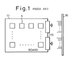
- a board 11 is connected to a mother-board 16 through a connector 15; the board 11 having dynamic elements 4 mounted thereon.
- the ground pins of the mother-board 16 are longer than the other pins, some of which supply electric power to the board 11 and some of which connect signal lines between the board 11 and mother-board 16.
- the board 11 is connected, first the ground pins are connected to the connectors 15.
- the circuit board assembly shown in Fig. 2 comprises a board 1 and a mother-board 6 serving as a power-supply unit for supplying power and control signals to the board 1.
- a clock distribution circuit 3 for permitting or preventing application of clock signals (CLK) to the dynamic elements 4 in response to "OFF" and "ON” operations respectively of a board exchange switch 2, and a connector 5 connecting the board 1 with the mother-board 6.
- the dynamic (clocked circuitry) elements 4 comprise CMOS circuits or Bi-CMOS circuits, which require only a very small electric current when in a non-operative state, i.e. when the clock signal is not supplied.
- a Bi-CMOS circuit comprises a CMOS circuit and a bipolar circuit.
- the clock distribution circuit 3 comprises a NAND gate 31 and buffer gates 32, receives clock signals from the connector 5, and distributes the clock signals to the plurality of dynamic elements 4, or stops the supply of the clock signals, in accordance with whether the board exchange switch 2 is set to the enable or disable state.
- the dynamic elements 4 supplied with the clock signals operate in synchronization with the clock.
- the electric current is larger than the current capacity of one pin of the connector 5 in the board 1, and therefore the electric current is supplied through a plurality of power source terminals and a plurality of ground terminals.
- the board exchange switch 2 is "ON"
- the clock distribution circuit is in the disabled state
- the switch 2 is "OFF"
- the clock distribution circuit is in the enable state.
- the connector 5 receives the large current flowing from the mother-board 6 to the board 1 through the power source supply terminals and the ground terminals and receives or supplies various signals from or to the mother-board 6.
- the connector 5 When the mother-board 6 is in the hot state, i.e. in the state in which power is supplied thereto, the connector 5 can be connected or disconnected from the board 1.
- the ground pin of the mother-board 6 is long and the power supply pins and the pins for the various signals are short. Accordingly, upon connection, first the ground pins are connected to the terminals of the connector 5 of the board 1, and then the power supply pins are connected to the terminals of the connector 5 of the board 1.
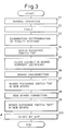
- step S1 the device is operating normally; i.e. the board 1 in Fig. 2 is connected to the mother-board 6 and is operating normally.
- step S2 assuming that a fault has occurred in the board 1 shown in Fig. 2 (e.g. parts breakdown, etc.), the board cannot operate normally.
- step S3 an examination is carried out, whereby a service processor SVP detects the fault and and determines which is the faulty board.
- step S4 the board exchange switch 2 is made “ON” (clock disable), so that in step S5 the clock signals are not supplied to the board 1, and the current flowing therethrough remains low. Since the board exchange switch 2 was made “ON” in step 4, the clock distribution circuit 3 stops the supply of clock signals to thc dynamic elements 4, and thus the electric current flowing through the power source terminals and the ground terminals of the connector 5 is lower than the current capacity of one terminal (or pin).
- step S6 the board 1 is disconnected, and since the current supplied through the connector 5 is lower than the capacity of one terminal of the connector 5, the board 1 can be disconnected from the mother-board 6 with little fear of damage thereto.
- step S7 the board exchange switch 2 of a new board is made "ON", and in step S8, the new board 1 is connected; i.e. the connector 5 of the new board 1 is connected to the mother-board 6, to replace the old faulty board 1.
- step S9 the board exchange switch 2 of the new board 1 is made "OFF", so that the new clock distribution circuit 3 starts to supply clock signals to the new dynamic elements 4.
- step 10 the new board 1 is operated by the SVP.
- the SVP operates the dynamic elements 4 supplied with clock signals after the initializing thereof.
- the board 1 can be set to a low current flow state or can be switched to the operating state by remote control from the SVP.
- the board when the board is connected or disconnected by setting the board exchange switch or by remote control, a low currnt flow state is set, and accordingly, the board can be connected to or disconnected safely from the mother-board 6. Therefore, since a large current does not flow through the ground terminals or the power source terminals of the connector 5, the board 1 can be connected or disconnected in the hot state, without damaging those terminals.
Landscapes
- Engineering & Computer Science (AREA)
- General Engineering & Computer Science (AREA)
- Theoretical Computer Science (AREA)
- Computer Hardware Design (AREA)
- Physics & Mathematics (AREA)
- General Physics & Mathematics (AREA)
- Mounting Of Printed Circuit Boards And The Like (AREA)
- Hardware Redundancy (AREA)
Applications Claiming Priority (2)
| Application Number | Priority Date | Filing Date | Title |
|---|---|---|---|
| JP293191/88 | 1988-11-19 | ||
| JP63293191A JPH02139610A (ja) | 1988-11-19 | 1988-11-19 | 活性着脱方式 |
Publications (2)
| Publication Number | Publication Date |
|---|---|
| EP0373773A1 true EP0373773A1 (fr) | 1990-06-20 |
| EP0373773B1 EP0373773B1 (fr) | 1995-03-01 |
Family
ID=17791599
Family Applications (1)
| Application Number | Title | Priority Date | Filing Date |
|---|---|---|---|
| EP89311923A Expired - Lifetime EP0373773B1 (fr) | 1988-11-19 | 1989-11-17 | Séparation de cartes de circuit électriques d'unités d'alimentation |
Country Status (4)
| Country | Link |
|---|---|
| US (1) | US5051606A (fr) |
| EP (1) | EP0373773B1 (fr) |
| JP (1) | JPH02139610A (fr) |
| DE (1) | DE68921441T2 (fr) |
Cited By (7)
| Publication number | Priority date | Publication date | Assignee | Title |
|---|---|---|---|---|
| EP0476394A3 (en) * | 1990-08-31 | 1992-10-28 | Fujitsu Limited | Clock distribution system |
| EP0552873A1 (fr) * | 1992-01-20 | 1993-07-28 | International Business Machines Corporation | Modification de la configuration système dans un système d'ordinateur |
| US6141711A (en) * | 1996-12-19 | 2000-10-31 | National Semiconductor Corporation | Method and apparatus to enable insertion/ejection of a device in a computer system while maintaining operation of the computer system and application software |
| US7565220B2 (en) | 2006-09-28 | 2009-07-21 | Lam Research Corporation | Targeted data collection architecture |
| US7672747B2 (en) | 2000-03-30 | 2010-03-02 | Lam Research Corporation | Recipe-and-component control module and methods thereof |
| US7814046B2 (en) | 2006-09-29 | 2010-10-12 | Lam Research Corporation | Dynamic component-tracking system and methods therefor |
| CN101145800B (zh) * | 2007-10-19 | 2011-03-02 | 中兴通讯股份有限公司 | 一种提高时钟板可靠切换的方法和装置 |
Families Citing this family (26)
| Publication number | Priority date | Publication date | Assignee | Title |
|---|---|---|---|---|
| JP2752247B2 (ja) * | 1990-11-29 | 1998-05-18 | 富士通株式会社 | 情報記憶装置 |
| US5583998A (en) * | 1991-12-20 | 1996-12-10 | Bull Hn Information Systems Inc. | Method and apparatus for increasing the speed of data exchange among the subsystems of a data processing system |
| JPH06132680A (ja) * | 1992-10-19 | 1994-05-13 | Nec Corp | プロテクト状態解除機構 |
| JP2864911B2 (ja) * | 1992-11-27 | 1999-03-08 | 三菱電機株式会社 | 活線挿抜方式 |
| US5575686A (en) * | 1993-04-14 | 1996-11-19 | Burndy Corporation | Stacked printed circuit boards connected in series |
| US6185723B1 (en) * | 1996-11-27 | 2001-02-06 | International Business Machines Corporation | Method for performing timing analysis of a clock-shaping circuit |
| US6014510A (en) * | 1996-11-27 | 2000-01-11 | International Business Machines Corporation | Method for performing timing analysis of a clock circuit |
| JP3034851B1 (ja) | 1998-10-15 | 2000-04-17 | ジーイー横河メディカルシステム株式会社 | Rfコイル並びに磁気共鳴撮像方法および装置 |
| US7047338B1 (en) * | 2000-07-18 | 2006-05-16 | Igt | Configurable hot-swap communication |
| US7441062B2 (en) | 2004-04-27 | 2008-10-21 | Apple Inc. | Connector interface system for enabling data communication with a multi-communication device |
| US7526588B1 (en) | 2004-04-27 | 2009-04-28 | Apple Inc. | Communication between an accessory and a media player using a protocol with multiple lingoes |
| US7441058B1 (en) | 2006-09-11 | 2008-10-21 | Apple Inc. | Method and system for controlling an accessory having a tuner |
| US7529870B1 (en) | 2004-04-27 | 2009-05-05 | Apple Inc. | Communication between an accessory and a media player with multiple lingoes |
| US7895378B2 (en) | 2004-04-27 | 2011-02-22 | Apple Inc. | Method and system for allowing a media player to transfer digital audio to an accessory |
| US7673083B2 (en) * | 2004-04-27 | 2010-03-02 | Apple Inc. | Method and system for controlling video selection and playback in a portable media player |
| US7529872B1 (en) | 2004-04-27 | 2009-05-05 | Apple Inc. | Communication between an accessory and a media player using a protocol with multiple lingoes |
| US8117651B2 (en) | 2004-04-27 | 2012-02-14 | Apple Inc. | Method and system for authenticating an accessory |
| US7457904B2 (en) * | 2004-12-16 | 2008-11-25 | Hewlett-Packard Development Company, L.P. | Methods and systems for a reference clock |
| US7823214B2 (en) | 2005-01-07 | 2010-10-26 | Apple Inc. | Accessory authentication for electronic devices |
| US8006019B2 (en) * | 2006-05-22 | 2011-08-23 | Apple, Inc. | Method and system for transferring stored data between a media player and an accessory |
| US7415563B1 (en) | 2006-06-27 | 2008-08-19 | Apple Inc. | Method and system for allowing a media player to determine if it supports the capabilities of an accessory |
| US7558894B1 (en) | 2006-09-11 | 2009-07-07 | Apple Inc. | Method and system for controlling power provided to an accessory |
| US8238811B2 (en) | 2008-09-08 | 2012-08-07 | Apple Inc. | Cross-transport authentication |
| US8208853B2 (en) | 2008-09-08 | 2012-06-26 | Apple Inc. | Accessory device authentication |
| CN110597670A (zh) * | 2019-08-13 | 2019-12-20 | 深圳震有科技股份有限公司 | 单板在位检测处理方法及装置、设备、介质 |
| KR20230161864A (ko) * | 2022-05-18 | 2023-11-28 | 창신 메모리 테크놀로지즈 아이엔씨 | 메모리 핫 플러그 방법 및 장치, 메모리 |
Citations (4)
| Publication number | Priority date | Publication date | Assignee | Title |
|---|---|---|---|---|
| US4200865A (en) * | 1977-02-02 | 1980-04-29 | Hitachi, Ltd. | Printed circuit board capable of being inserted and withdrawn on on-line status |
| US4510553A (en) * | 1983-01-24 | 1985-04-09 | Burroughs Corporation | Electromechanical assembly for aligning, discharging, and sequentially engaging conductors of a P.C. board with a backplane |
| EP0241905A2 (fr) * | 1986-04-14 | 1987-10-21 | Siemens Nixdorf Informationssysteme Aktiengesellschaft | Plaquette de circuit pour insertion en ligne dans un système ordinateur |
| EP0254456A2 (fr) * | 1986-07-21 | 1988-01-27 | AT&T Corp. | Appareil pour l'enlèvement et l'insertion contrôlés de modules à circuits électriques |
-
1988
- 1988-11-19 JP JP63293191A patent/JPH02139610A/ja active Pending
-
1989
- 1989-11-13 US US07/434,754 patent/US5051606A/en not_active Expired - Fee Related
- 1989-11-17 EP EP89311923A patent/EP0373773B1/fr not_active Expired - Lifetime
- 1989-11-17 DE DE68921441T patent/DE68921441T2/de not_active Expired - Fee Related
Patent Citations (4)
| Publication number | Priority date | Publication date | Assignee | Title |
|---|---|---|---|---|
| US4200865A (en) * | 1977-02-02 | 1980-04-29 | Hitachi, Ltd. | Printed circuit board capable of being inserted and withdrawn on on-line status |
| US4510553A (en) * | 1983-01-24 | 1985-04-09 | Burroughs Corporation | Electromechanical assembly for aligning, discharging, and sequentially engaging conductors of a P.C. board with a backplane |
| EP0241905A2 (fr) * | 1986-04-14 | 1987-10-21 | Siemens Nixdorf Informationssysteme Aktiengesellschaft | Plaquette de circuit pour insertion en ligne dans un système ordinateur |
| EP0254456A2 (fr) * | 1986-07-21 | 1988-01-27 | AT&T Corp. | Appareil pour l'enlèvement et l'insertion contrôlés de modules à circuits électriques |
Cited By (11)
| Publication number | Priority date | Publication date | Assignee | Title |
|---|---|---|---|---|
| EP0476394A3 (en) * | 1990-08-31 | 1992-10-28 | Fujitsu Limited | Clock distribution system |
| US5274677A (en) * | 1990-08-31 | 1993-12-28 | Fujitsu Limited | Clock distribution system |
| EP0552873A1 (fr) * | 1992-01-20 | 1993-07-28 | International Business Machines Corporation | Modification de la configuration système dans un système d'ordinateur |
| US6141711A (en) * | 1996-12-19 | 2000-10-31 | National Semiconductor Corporation | Method and apparatus to enable insertion/ejection of a device in a computer system while maintaining operation of the computer system and application software |
| DE19737214B4 (de) * | 1996-12-19 | 2007-01-04 | National Semiconductor Corp.(N.D.Ges.D.Staates Delaware), Santa Clara | Verfahren zum Betreiben eines Computersystems, Computersystem und Sekundärbus-Controller |
| US7672747B2 (en) | 2000-03-30 | 2010-03-02 | Lam Research Corporation | Recipe-and-component control module and methods thereof |
| US7565220B2 (en) | 2006-09-28 | 2009-07-21 | Lam Research Corporation | Targeted data collection architecture |
| US7814046B2 (en) | 2006-09-29 | 2010-10-12 | Lam Research Corporation | Dynamic component-tracking system and methods therefor |
| US8010483B2 (en) | 2006-09-29 | 2011-08-30 | Lam Research Corporation | Component-tracking system and methods therefor |
| US8295963B2 (en) | 2007-03-29 | 2012-10-23 | Lam Research Corporation | Methods for performing data management for a recipe-and-component control module |
| CN101145800B (zh) * | 2007-10-19 | 2011-03-02 | 中兴通讯股份有限公司 | 一种提高时钟板可靠切换的方法和装置 |
Also Published As
| Publication number | Publication date |
|---|---|
| JPH02139610A (ja) | 1990-05-29 |
| US5051606A (en) | 1991-09-24 |
| DE68921441T2 (de) | 1995-06-29 |
| EP0373773B1 (fr) | 1995-03-01 |
| DE68921441D1 (de) | 1995-04-06 |
Similar Documents
| Publication | Publication Date | Title |
|---|---|---|
| EP0373773A1 (fr) | Séparation de cartes de circuit électriques d'unités d'alimentation | |
| US9997957B2 (en) | Auto-switching duplex module | |
| US6591324B1 (en) | Hot swap processor card and bus | |
| US6661119B2 (en) | System and method for distributed power supply supporting high currents with redundancy | |
| CN109710046B (zh) | 框式设备业务板上下电控制系统、方法、装置及主控板 | |
| USRE39855E1 (en) | Power management strategy to support hot swapping of system blades during run time | |
| US6189058B1 (en) | Crossbar connect switch mechanism for hot plugability | |
| CN100512135C (zh) | 一种通讯设备电源管理系统及其实现方法 | |
| US6801973B2 (en) | Hot swap circuit module | |
| EP0677225B1 (fr) | Systeme de production de tension dans une ligne de tension commune a une pluralite d'unites electriques | |
| US20070285851A1 (en) | Apparatus and method for cold sparing in multi-board computer systems | |
| JP4459408B2 (ja) | ホットスワップバス | |
| US5463663A (en) | Controlling synchronization in a system having a plurality of units when a unit is disconnected from or connected to the system that is active | |
| EP1176514B1 (fr) | Carte processeur échangeable sous tension et bus | |
| CN112968590A (zh) | 一种兼容性供电装置和服务器 | |
| KR0182687B1 (ko) | 보드탈장에 의한 이중화 제어장치 | |
| KR100195077B1 (ko) | 랜의 접속장치 | |
| US20200233476A1 (en) | Computer system and system board | |
| JPH0752377B2 (ja) | 電子回路基板 | |
| JPS63298511A (ja) | 電源装置 | |
| JP3269291B2 (ja) | 活線挿抜方式 | |
| JP2685761B2 (ja) | 接続ケーブル | |
| JP3042522B1 (ja) | プリント基板の異同検知機構 | |
| US20050093513A1 (en) | Electronic device having multiple current outputs | |
| JPH07182074A (ja) | ホットスタンバイ式デュプレックスシステムの活線挿抜装置 |
Legal Events
| Date | Code | Title | Description |
|---|---|---|---|
| PUAI | Public reference made under article 153(3) epc to a published international application that has entered the european phase |
Free format text: ORIGINAL CODE: 0009012 |
|
| AK | Designated contracting states |
Kind code of ref document: A1 Designated state(s): DE FR GB |
|
| 17P | Request for examination filed |
Effective date: 19900807 |
|
| 17Q | First examination report despatched |
Effective date: 19930315 |
|
| GRAA | (expected) grant |
Free format text: ORIGINAL CODE: 0009210 |
|
| AK | Designated contracting states |
Kind code of ref document: B1 Designated state(s): DE FR GB |
|
| REF | Corresponds to: |
Ref document number: 68921441 Country of ref document: DE Date of ref document: 19950406 |
|
| ET | Fr: translation filed | ||
| PLBE | No opposition filed within time limit |
Free format text: ORIGINAL CODE: 0009261 |
|
| STAA | Information on the status of an ep patent application or granted ep patent |
Free format text: STATUS: NO OPPOSITION FILED WITHIN TIME LIMIT |
|
| 26N | No opposition filed | ||
| PGFP | Annual fee paid to national office [announced via postgrant information from national office to epo] |
Ref country code: FR Payment date: 20001110 Year of fee payment: 12 |
|
| PGFP | Annual fee paid to national office [announced via postgrant information from national office to epo] |
Ref country code: DE Payment date: 20001113 Year of fee payment: 12 |
|
| PGFP | Annual fee paid to national office [announced via postgrant information from national office to epo] |
Ref country code: GB Payment date: 20001115 Year of fee payment: 12 |
|
| PG25 | Lapsed in a contracting state [announced via postgrant information from national office to epo] |
Ref country code: GB Free format text: LAPSE BECAUSE OF NON-PAYMENT OF DUE FEES Effective date: 20011117 |
|
| REG | Reference to a national code |
Ref country code: GB Ref legal event code: IF02 |
|
| PG25 | Lapsed in a contracting state [announced via postgrant information from national office to epo] |
Ref country code: DE Free format text: LAPSE BECAUSE OF NON-PAYMENT OF DUE FEES Effective date: 20020702 |
|
| GBPC | Gb: european patent ceased through non-payment of renewal fee |
Effective date: 20011117 |
|
| PG25 | Lapsed in a contracting state [announced via postgrant information from national office to epo] |
Ref country code: FR Free format text: LAPSE BECAUSE OF NON-PAYMENT OF DUE FEES Effective date: 20020730 |
|
| REG | Reference to a national code |
Ref country code: FR Ref legal event code: ST |
|
| REG | Reference to a national code |
Ref country code: FR Ref legal event code: ST |