EP0373786B1 - Dispositif d'affichage - Google Patents
Dispositif d'affichage Download PDFInfo
- Publication number
- EP0373786B1 EP0373786B1 EP89312381A EP89312381A EP0373786B1 EP 0373786 B1 EP0373786 B1 EP 0373786B1 EP 89312381 A EP89312381 A EP 89312381A EP 89312381 A EP89312381 A EP 89312381A EP 0373786 B1 EP0373786 B1 EP 0373786B1
- Authority
- EP
- European Patent Office
- Prior art keywords
- pulse
- cell
- pulses
- state
- liquid crystal
- Prior art date
- Legal status (The legal status is an assumption and is not a legal conclusion. Google has not performed a legal analysis and makes no representation as to the accuracy of the status listed.)
- Expired - Lifetime
Links
- 230000005540 biological transmission Effects 0.000 claims abstract description 36
- 239000005262 ferroelectric liquid crystals (FLCs) Substances 0.000 claims abstract description 26
- 238000000034 method Methods 0.000 claims abstract description 24
- 230000005670 electromagnetic radiation Effects 0.000 claims abstract description 7
- 239000004973 liquid crystal related substance Substances 0.000 claims description 39
- 210000004027 cell Anatomy 0.000 claims description 26
- 210000002858 crystal cell Anatomy 0.000 claims description 9
- 230000003287 optical effect Effects 0.000 description 42
- 239000000463 material Substances 0.000 description 18
- 230000000694 effects Effects 0.000 description 12
- 230000015556 catabolic process Effects 0.000 description 5
- 238000006731 degradation reaction Methods 0.000 description 5
- 239000011521 glass Substances 0.000 description 5
- 230000006641 stabilisation Effects 0.000 description 5
- 238000000926 separation method Methods 0.000 description 3
- AMGQUBHHOARCQH-UHFFFAOYSA-N indium;oxotin Chemical compound [In].[Sn]=O AMGQUBHHOARCQH-UHFFFAOYSA-N 0.000 description 2
- 230000002427 irreversible effect Effects 0.000 description 2
- 239000000203 mixture Substances 0.000 description 2
- 230000000704 physical effect Effects 0.000 description 2
- 230000005855 radiation Effects 0.000 description 2
- 238000011105 stabilization Methods 0.000 description 2
- 239000004677 Nylon Substances 0.000 description 1
- 239000004642 Polyimide Substances 0.000 description 1
- 239000000853 adhesive Substances 0.000 description 1
- 230000001070 adhesive effect Effects 0.000 description 1
- 230000001419 dependent effect Effects 0.000 description 1
- 230000006866 deterioration Effects 0.000 description 1
- 230000005684 electric field Effects 0.000 description 1
- 238000003487 electrochemical reaction Methods 0.000 description 1
- 230000002045 lasting effect Effects 0.000 description 1
- 238000001208 nuclear magnetic resonance pulse sequence Methods 0.000 description 1
- 229920001778 nylon Polymers 0.000 description 1
- 239000000049 pigment Substances 0.000 description 1
- 229920001721 polyimide Polymers 0.000 description 1
- 238000002360 preparation method Methods 0.000 description 1
- 230000002441 reversible effect Effects 0.000 description 1
- 239000000758 substrate Substances 0.000 description 1
Images


Classifications
-
- G—PHYSICS
- G09—EDUCATION; CRYPTOGRAPHY; DISPLAY; ADVERTISING; SEALS
- G09G—ARRANGEMENTS OR CIRCUITS FOR CONTROL OF INDICATING DEVICES USING STATIC MEANS TO PRESENT VARIABLE INFORMATION
- G09G3/00—Control arrangements or circuits, of interest only in connection with visual indicators other than cathode-ray tubes
- G09G3/20—Control arrangements or circuits, of interest only in connection with visual indicators other than cathode-ray tubes for presentation of an assembly of a number of characters, e.g. a page, by composing the assembly by combination of individual elements arranged in a matrix no fixed position being assigned to or needed to be assigned to the individual characters or partial characters
- G09G3/34—Control arrangements or circuits, of interest only in connection with visual indicators other than cathode-ray tubes for presentation of an assembly of a number of characters, e.g. a page, by composing the assembly by combination of individual elements arranged in a matrix no fixed position being assigned to or needed to be assigned to the individual characters or partial characters by control of light from an independent source
- G09G3/36—Control arrangements or circuits, of interest only in connection with visual indicators other than cathode-ray tubes for presentation of an assembly of a number of characters, e.g. a page, by composing the assembly by combination of individual elements arranged in a matrix no fixed position being assigned to or needed to be assigned to the individual characters or partial characters by control of light from an independent source using liquid crystals
- G09G3/3611—Control of matrices with row and column drivers
- G09G3/3622—Control of matrices with row and column drivers using a passive matrix
- G09G3/3629—Control of matrices with row and column drivers using a passive matrix using liquid crystals having memory effects, e.g. ferroelectric liquid crystals
-
- G—PHYSICS
- G09—EDUCATION; CRYPTOGRAPHY; DISPLAY; ADVERTISING; SEALS
- G09G—ARRANGEMENTS OR CIRCUITS FOR CONTROL OF INDICATING DEVICES USING STATIC MEANS TO PRESENT VARIABLE INFORMATION
- G09G2310/00—Command of the display device
- G09G2310/06—Details of flat display driving waveforms
-
- G—PHYSICS
- G09—EDUCATION; CRYPTOGRAPHY; DISPLAY; ADVERTISING; SEALS
- G09G—ARRANGEMENTS OR CIRCUITS FOR CONTROL OF INDICATING DEVICES USING STATIC MEANS TO PRESENT VARIABLE INFORMATION
- G09G2310/00—Command of the display device
- G09G2310/06—Details of flat display driving waveforms
- G09G2310/065—Waveforms comprising zero voltage phase or pause
Definitions
- This invention relates to a method of addressing a ferroelectric liquid crystal device (FLCD), in particular to a method of controlling the transmission of electromagnetic radiation through such a device.
- FLCD ferroelectric liquid crystal device
- This method is particularly, though not exclusively, intended for addressing such a device used as an optical shutter. It is envisaged that such a method could be used to control the transmission through a FLCD of electromagnetic radiation of other wavelengths e.g. infra-red and ultra-violet radiation as well as optical radiation.
- Ferroelectric liquid crystal materials have a DC voltage response.
- An FLCD containing such a material between polarizers can be switched from a light transmissive state to a non-transmissive state and vice versa by an applied voltage of sufficient magnitude and pulse width, the state into which it is switched being dependent upon the polarity of the applied voltage.
- a variety of voltage waveforms can be used but a waveform with a step function, e.g. a square wave pulse, is preferred for a minimum rise and fall time (fast response).
- Figure 1 shows an electro-optic characteristic, i.e.
- Figure 2 shows a graph of voltage applied to a ferroelectric liquid crystal layer against time and a graph of optical transmission of that liquid crystal layer over the same time.
- Monopolar pulses of sufficient pulse height V S and pulse width t S to switch the liquid crystal layer between a first state T X1 of maximum optical transmission and a second state T X2 of minimum optical transmission are applied.
- the ideal optical transmission curve is shown in dotted lines - the liquid crystal is latched in the first or second state until a pulse of the polarity required to switch it into the other state is applied.
- some relaxation of the latched states usually occurs within a period of 10t S and the separation of the monopolar pulses is greater than this.
- the continuous curve of Figure 2 shows this relaxation which reduces the contrast ratio, an undesirable effect for a light shutter.
- the device is switched between the first and second states T x1 , T x2 by a continuously applied AC square wave voltage.
- the AC square wave voltage pulses are of sufficient height V S and pulse width t S to switch between the first and second states.
- the applied voltage V s prevents relaxation occurring and maintains the liquid crystal cell in the T x1 or T x2 state, ensuring that the contrast remains high.
- the alignment of the liquid crystal layer in the device can easily be damaged in an irreversible manner when alternating electric fields above a critical value are applied. Alignment damage to the liquid crystal layer reduces the contrast ratio of the shutter and tends to increase the response time of the material.
- the critical value is typically of the order of 10V/»m - well below that usually required to realise the maximum switching speed.
- a high frequency background AC signal of voltage magnitude V AC is applied to stabilise the states T X1 and T X2 .
- V AC has a finite value V a
- there is stabilisation whereas when V AC 0, relaxation occurs.
- the value of the fields necessary for AC stabilisation can depend on a variety of parameters such as cell thickness, preparation of the alignment layer material and physical properties of the liquid crystal material, such as its dielectric anisotropy e.g. as disclosed by T.Umeda et al : Influences of Alignment Materials and LC Layer Thickness on AC Field - Stabilization Phenomena of Ferroelectric Liquid Crystals (Japanese Journal of Applied Physics Vol. 27. No. 7.
- GB 2175725A discloses a method of driving an electro-optical display device (such as an FLCD) for producing a display consisting of display elements and which comprises first and second sets of electrodes, the electrodes of one set crossing those of the other.
- a selection signal is sequentially applied to the first set of electrodes while a non-selection signal is applied to each of the first set of electrodes to which the selection signal is not applied.
- the resultant waveform across that display element is a substantially true pulsed AC waveform.
- this substantially true pulsed AC waveform comprises two pulses of one polarity having a reduced duration half or less than half of the duration of the switching pulse followed by two pulses of the same reduced duration but of the other polarity.
- the provision of a substantially time pulsed AC waveform ensures that the substantially transparent electrodes do not become blackened, the liquid crystal material does not deteriorate and double colour pigment does not become discoloured, even after driving for a long time.
- the AC waveform provided during non-selection also provides good contrast.
- US 4508429 (Nagae et al) dislose a FLC display in which two light transmitting states, i.e. a bright state and a dark state, can be established. Each of these states is defined by the average brightness brought about by pulse voltage trains of a respective polarity. Each pulse in the pulse voltage trains shown is of the same pulse height which is accordingly sufficient to switch the FLC display from one defined light transmitting state to the other and vice versa.
- a problem with this driving method is that, unless the duration of the bright display state is equal to that of the dark display state, the voltage V LC applied to the FLC will include a DC component.
- US 4508429 disloses that 'It is well known that when a DC component is applied to a liquid crystal element during the driving thereof, the deterioration of the element is accelerated because of an electrochemical reaction, thereby resulting in a reduced life.
- US-A-4,701,026 discloses a method of multiplex-addressing a liquid crystal cell in which a switching pulse is followed by data pulses of the same pulse-height as the switching pulse.
- a method of controlling the transmission of electromagnetic radiation through a ferroelectric liquid crystal device comprising at least one liquid crystal cell having a first state of maximum transmission and a further state of minimum transmission the cell being switchable between the first and further states by application thereto of a switching voltage pulse having a width and height which, in combination, are sufficient to switch the cell; the method including: applying a first such switching pulse of one polarity to the cell and thereafter, for a time period greater than the value of the switching pulse width, applying a first plurality of consecutive unipolar controlling pulses to the cell, each controlling pulse having a height and width which, in combination, are insufficient to switch the cell between the first and further states; characterised in that each controlling pulse of the plurality of controlling pulses has a height less thanthe height of the associated switching pulse, the first plurality of controlling pulses thereby serving to control the transmission of the cell in its current state by counteracting any relaxation of this state.
- a scheme according to the present invention permits quasi-analogue control of the transmission of electromagnetic radiation through a ferroelectric liquid crystal device.
- the unipolar controlling pulses of the first plurality are not all of the same polarity.
- the switching pulse can be used to switch at high speed in a digital fashion between the first and second states while the controlling pulses can be used to control the transmission of electromagnetic radiation through the device once it is in the first or second state.
- the step of applying said switching pulse is followed by the step of applying a plurality of consecutive controlling pulses of the same polarity as said switching pulse whereby the cell is maintained in one of said first or said second states.
- a cell addressed by such a method has a high contrast ratio and the quick response produced by the switching pulse.
- An optical shutter may be driven by an addressing scheme in which the steps of applying a switching pulse of one polarity and a plurality of consecutive controlling pulses of the same polarity as said switching pulse is followed by the steps of applying a switching pulse of the other polarity and a plurality of consecutive controlling pulses of that other polarity.
- the period for which pulses of one polarity are applied may be equal to the period for which pulses of the other polarity are applied, resulting in the optical shutter being in the states of maximum and minimum transmission for equal periods of time and in a DC compensated waveform.
- the optical shutter may be driven by an addressing scheme in which the period for which pulses of one polarity are applied is not equal to the period for which pulses of the other polarity are applied and so the optical shutter is in the states of maximum and minimum transmission for unequal periods of time.
- the inventor has surprisingly found that the present invention can provide an addressing scheme in which the problems of degradation of alignment due to DC electrolytic effects can be alleviated without the need to ensure that the waveform is DC compensated overall.
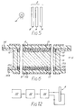
- FIG. 5 shows an optical shutter 2 in front of a light source shown schematically at 4.
- the optical shutter 2 is shown in an exploded view and comprises a ferroelectric liquid crystal cell 6 on either side of which is a polarizer 8, 9.
- the polarizers are usually crossed.
- the shutter 2 has a first state T X1 of maximum optical transmission and a second state T X2 of minimum optical transmission.
- Application of a voltage pulse of sufficient pulse height V S and pulse width t S and of the correct polarity switches the shutter 2 from the first state to the second state or vice versa.
- FIG. 6 shows the ferroelectric liquid crystal cell 6 of Figure 5 in greater detail.
- the cell 6 consists of two glass plates 11, 11a each coated with a transparent conducting electrode 12, 12a formed of indium tin oxide and an alignment layer 13, 13a, typically of nylon or polyimide, rubbed unidirectionally. Insulating layers 14, 14a and 15, 15a can be used respectively to separate the glass substrate 11, 11a from the electrode 12, 12a and the electrode 12, 12a from the alignment layer 13, 13a.
- the two glass plates 11, 11a are spaced 1.5 »m apart and are sealed around the perimeter with an adhesive edge seal 16 which holds the glass plates together.
- the indium tin oxide is patterned to define a single active element which can be directly driven by an applied voltage.
- a ferroelectric liquid crystal material 17, such as SCE13 supplied by BDH Ltd., Poole, UK
- SCE13 supplied by BDH Ltd., Poole, UK
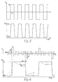
- FIG. 7 shows an addressing scheme provided in accordance with the present invention which can be used to address the shutter of Figure 5 and maintain a high contrast ratio.
- the scheme is a waveform comprising single high voltage switching pulses 20 followed by a series of consecutive low voltage pulses 22 of the same polarity and a separation and pulse width typically the same as the pulse width of the switching pulse 20.
- the switching pulses have a pulse height V S and a pulse width t S such that the shutter can be switched from the first state to the second state or vice versa in the minimum time possible. Once the shutter has been switched into the first or the second state, in the absence of any applied voltage it would tend to relax as mentioned hereinbefore.
- the low voltage pulses 22 control the optical transmission of the shutter by continually driving the device back into the first or second state before any significant relaxation can occur and so are effective as latching pulses.
- the latching pulses 22 prevent or at least reduce any relaxation of the first and second states, they ensure that the contrast ratio of the shutter remains as high as possible.
- the use of discrete latching pulses 22 can result in optical noise (i.e. the optical transmission T X will try to follow the instantaneous value of the applied voltage). This problem can be alleviated by keeping the pulse height-pulse width product for each latching pulse 22 to a minimum.
- the use of a plurality of low voltage latching pulses of one polarity can cause DC electrolytic effects within the liquid crystal material, which can lead to alignment damage to the liquid crystal layer. Such effects can be reduced by using latching pulses of pulse-widths similar to or smaller than the pulse width t S of the switching pulse. It is believed that this improvement is due to the use of pulses of low pulse width, reducing the time during which charge can accumulate at the surfaces of the liquid crystal layer and allowing time between pulses for any accumulated charge to disperse before any irreversible distortion occurs in the alignment of the liquid crystal layer.
- the pulse height used for the latching pulses is chosen to minimise the relaxation process without degradation of the alignment due to AC fields or any DC electrolytic effects. For some liquid crystal mixtures, if the pulse heights and pulse widths are carefully chosen, sequences of latching pulses of the same polarity lasting a few seconds can be achieved without causing DC alignment damage.
- a shutter comprising a 1.5 »m thick cell containing the liquid crystal material SCE13 (supplied by BDH Ltd., Poole, UK) was operated at a temperature of 25°C and a frequency of switching of 0.5Hz.
- the switching pulses were of pulse height 50V and pulse width about 15 »s.
- the latching pulses were of pulse height 5V with a pulse width and separation of about 15 »s.
- Figure 8 illustrates the use of controlling pulses 24 in waveforms to control the optical transmission of the shutter.
- Switching pulses 26 of pulse height V S and pulse width t S can be used to switch the shutter from the state T X1 to the state T X2 and vice versa in the minimum time possible.
- Pulses of varying heights can be used to control the rate of change of optical transmission though it is envisaged that there is a minimum pulse height for a pulse below which the effect is negligible.
- Pulses of different polarities can be used to increase and decrease the optical transmission.
- the pulse heights and pulse widths should be chosen to avoid or at least alleviate potential alignment damage to the liquid crystal layer by DC or AC effects.
- the controlling pulse magnitude should be kept below the critical value for AC damage, typically about 10V/»m, though a few isolated controlling pulses can be similar in pulse height magnitude to that of the switching pulse.
- sequences of pulses of alternating polarity with a pulse height magnitude greater than the critical value should be kept to a minimum as this can cause AC alignment damage effects.
- the pulse width of the controlling pulses should be kept similar or smaller than the pulse width t S of the switching pulse, as defined by the electro-optic characteristic of the liquid crystal material, e.g. as shown in Figure 1.
- Figure 10 shows an optical response for a shutter addressed by the scheme of Figure 9 in which the mark-to-space ratio is 10:1.
- the mark-to-space ratio is 10:1.
- FIG. 11a shows the optical transmission T X of the liquid crystal optical shutter over time for an exposure of the film whilst Figure 11b shows (not to the same time scale) the voltage waveforms used to produced this effect.
- the state of the liquid crystal optical shutter is not important and can be unspecified.
- the liquid crystal optical shutter is switched to the dark state T X2 .
- the liquid crystal optical shutter is being maintained in the dark state T X2 by latching pulses 27, pulse height V L , pulse width t L of one polarity.
- a switching pulse 28 of the other polarity is applied to switch the liquid crystal optical shutter into the state T X1 of maximum transmission (light state) and so expose the film.
- latching pulses 28a of the same polarity as the switching pulse may be applied, if necessary (as shown) to maintain the shutter in the T X1 state.
- time t3 the liquid crystal optical shutter is switched back to the dark state T X2 by a switching pulse 29 and latching pulses 29a are applied to maintain the liquid crystal optical shutter in the dark state until the mechanical shutter is closed at time t4.
- the voltage applied to the liquid crystal optical shutter can then be removed.
- the exposure time (t3-t2) will depend upon the switching speed of the liquid crystal, the light transmitted through the liquid crystal optical shutter and the speed of the film.
- the waveform applied to the liquid crystal material for the camera system is a 'single-shot' waveform, i.e. the waveform is not being continually repeated or cycled. Accordingly, a mark-to-space ratio well in excess of the previously mentioned 10:1 (1000:1 in this example) is permitted as any cell alignment degradation due to DC electrolytic effects will occur over a considerably longer time scale than the shutter time of a high speed camera.
- the contrast ratio of the liquid crystal optical shutter, the light transmitted by the liquid crystal in the dark state and the speed of the film will limit the maximum mark-to-space ratio.
- a suitable circuit for generating waveforms to address the shutter of Figure 5 is shown schematically in Figure 12.
- the required waveform is generated by a computer programme loaded into a computer 30 (e.g. a Hewlett-Packard 9000/300) which determines the relative pulse heights at each of a number of time slots of the waveform produced by an arbitrary waveform generator 32 (eg a Wavetek Model 275 12MHz programmeable arbitrary function generator).
- the arbitrary waveform generator 32 is able to generate voltages in the range ⁇ 10V.
- the output of the arbitrary waveform generator 32 is fed to a voltage amplifier 34, capable of generating voltages in the range ⁇ 80V, to generate the required waveform across the ferroelectric liquid crystal cell 6.
Landscapes
- Engineering & Computer Science (AREA)
- Theoretical Computer Science (AREA)
- Physics & Mathematics (AREA)
- Crystallography & Structural Chemistry (AREA)
- Computer Hardware Design (AREA)
- General Physics & Mathematics (AREA)
- Chemical & Material Sciences (AREA)
- Liquid Crystal Display Device Control (AREA)
- Liquid Crystal (AREA)
- Control Of Indicators Other Than Cathode Ray Tubes (AREA)
- Circuits Of Receivers In General (AREA)
- Liquid Crystal Substances (AREA)
- Control Of El Displays (AREA)
- Control Of Gas Discharge Display Tubes (AREA)
Claims (9)
- Procédé pour commander la transmission d'un rayonnement électromagnétique à travers un dispositif à cristal liquide ferroélectrique comprenant au moins une cellule à cristal liquide (6) pouvant prendre un premier état de transmission maximum (TX1) et un autre état de transmission minimum (TX2), la cellule pouvant être commutée entre le premier état et l'autre état par application à cette cellule d'une impulsion de tension de commutation (20) ayant une largeur (ts) et une hauteur (Vs) qui, en combinaison, sont suffisantes pour commuter la cellule (6) ; le procédé comprenant les phase consistant à : appliquer une première impulsion de commutation (20) de ce type, d'une certaine polarité à la cellule et, ensuite, pendant un temps supérieur à la valeur de la largeur (tS) des impulsions de commutation, appliquer une première pluralité d'impulsions de commande unipolaires consécutives (22) à la cellule, chaque impulsion de commande (22) ayant une hauteur (VL) et une largeur (tL) qui, en combinaison, sont insuffisantes pour commuter la cellule (6) entre le premier état (TX1) et l'autre état (TX2), caractérisé en ce que chaque impulsion de commande (22) d'une pluralité d'impulsions de commande a une hauteur inférieure à la hauteur de l'impulsion de commutation (20) associée, à la première pluralité d'impulsions de commande (22) servant ainsi à commander la transmission de la cellule (6) dans son état actuel en contrariant l'éventuelle relaxation de cet état.
- Procédé selon la revendication 1, dans lequel les impulsions de commande unipolaires (22) d'une première pluralité ne sont pas toutes de la même polarité.
- Procédé selon la revendication 1, dans lequel, à la suite de l'application de l'impulsion de commutation (20) à la cellule (6), une autre impulsion de commutation (20) de la polarité opposée est appliquée à la cellule (6), suivie d'une autre pluralité d'impulsions de commande unipolaires consécutives de la même polarité que l'autre impulsion de commutation (20).
- Procédé selon la revendication 1, dans lequel, à la suite de l'application de l'impulsion de commutation (20) à la cellule (6), une autre impulsion de commutation (20) de la polarité opposée est appliquée à la cellule (6), ceci étant suivi d'une autre pluralité d'impulsions de commande unipolaires consécutives de la polarité opposée de celle de l'autre impulsion de commutation (20).
- Procédé selon la revendication 3 ou la revendication 4, dans lequel la première et l'autre pluralité d'impulsions de commande (22) sont appliquées à la cellule (6) pendant des périodes sensiblement égales.
- Procédé selon la revendication 1, dans lequel les impulsions de commande (22) de la première pluralité ont chacune une largeur sensiblement égale à la largeur de la première impulsion de commutation (20).
- Procédé selon la revendication 3 ou la revendication 4, dans lequel les impulsions de commande de l'autre pluralité ont une largeur sensiblement égale à la largeur de la première impulsion de commutation.
- Procédé selon la revendication 1, dans lequel les impulsions de commande de la première pluralité ont un rapport de marque-espacement de 1:1.
- Procédé selon la revendication 3 ou la revendication 4, dans lequel les impulsions de commande de l'autre pluralité ont un rapport marque-espacement de 1:1.
Applications Claiming Priority (4)
| Application Number | Priority Date | Filing Date | Title |
|---|---|---|---|
| GB8829129 | 1988-12-14 | ||
| GB888829129A GB8829129D0 (en) | 1988-12-14 | 1988-12-14 | Display device |
| GB8914836 | 1989-06-28 | ||
| GB898914836A GB8914836D0 (en) | 1989-06-28 | 1989-06-28 | Display device |
Publications (3)
| Publication Number | Publication Date |
|---|---|
| EP0373786A2 EP0373786A2 (fr) | 1990-06-20 |
| EP0373786A3 EP0373786A3 (fr) | 1991-08-14 |
| EP0373786B1 true EP0373786B1 (fr) | 1995-02-22 |
Family
ID=26294727
Family Applications (1)
| Application Number | Title | Priority Date | Filing Date |
|---|---|---|---|
| EP89312381A Expired - Lifetime EP0373786B1 (fr) | 1988-12-14 | 1989-11-29 | Dispositif d'affichage |
Country Status (8)
| Country | Link |
|---|---|
| US (1) | US5111317A (fr) |
| EP (1) | EP0373786B1 (fr) |
| JP (1) | JP2927471B2 (fr) |
| AT (1) | ATE118916T1 (fr) |
| CA (1) | CA2005403C (fr) |
| DE (1) | DE68921310T2 (fr) |
| DK (1) | DK632989A (fr) |
| NO (1) | NO894900L (fr) |
Families Citing this family (15)
| Publication number | Priority date | Publication date | Assignee | Title |
|---|---|---|---|---|
| DE4123696A1 (de) * | 1991-07-17 | 1993-01-21 | Merck Patent Gmbh | Ansteuerungsverfahren |
| US5703615A (en) * | 1992-02-10 | 1997-12-30 | Fuji Photo Film Co., Ltd. | Method for driving matrix type flat panel display device |
| JPH0683297A (ja) * | 1992-09-03 | 1994-03-25 | Ricoh Co Ltd | 表示制御装置およびその表示制御方法 |
| GB2271011A (en) * | 1992-09-23 | 1994-03-30 | Central Research Lab Ltd | Greyscale addressing of ferroelectric liquid crystal displays. |
| US5673062A (en) * | 1992-11-06 | 1997-09-30 | Canon Kabushiki Kaisha | Liquid crystal apparatus |
| US5532713A (en) * | 1993-04-20 | 1996-07-02 | Canon Kabushiki Kaisha | Driving method for liquid crystal device |
| JP3054520B2 (ja) * | 1993-10-06 | 2000-06-19 | シャープ株式会社 | アクティブマトリックスセルの駆動方法 |
| GB2293906A (en) * | 1994-10-03 | 1996-04-10 | Sharp Kk | Liquid crystal display |
| GB9503858D0 (en) * | 1995-02-25 | 1995-04-19 | Central Research Lab Ltd | Drive circuit |
| SE509569C2 (sv) * | 1995-10-26 | 1999-02-08 | Hoernell International Ab | Vätskekristallslutarkonstruktion |
| US6753909B1 (en) * | 1999-04-20 | 2004-06-22 | Sharp Laboratories Of America, Inc. | Camera with spatially adjustable variable density optical filter and method for controlling the same |
| US6507330B1 (en) | 1999-09-01 | 2003-01-14 | Displaytech, Inc. | DC-balanced and non-DC-balanced drive schemes for liquid crystal devices |
| AU7335200A (en) * | 1999-09-01 | 2001-03-26 | Display Tech, Inc. | Reduction of effects caused by imbalanced driving of liquid crystal cells |
| US20120169691A1 (en) * | 2010-12-30 | 2012-07-05 | Zebra Imaging, Inc. | DC-Balancing a Display between Sets of Frames |
| RU2697888C1 (ru) * | 2018-12-20 | 2019-08-21 | Федеральное государственное бюджетное учреждение науки Физический институт им. П.Н. Лебедева Российской академии наук (ФИАН) | Способ управления сегнетоэлектрическим жидкокристаллическим затвором |
Family Cites Families (11)
| Publication number | Priority date | Publication date | Assignee | Title |
|---|---|---|---|---|
| JPH0629919B2 (ja) * | 1982-04-16 | 1994-04-20 | 株式会社日立製作所 | 液晶素子の駆動方法 |
| JPS6015624A (ja) * | 1983-07-08 | 1985-01-26 | Hitachi Ltd | 液晶プリンタの駆動方法 |
| US4701026A (en) * | 1984-06-11 | 1987-10-20 | Seiko Epson Kabushiki Kaisha | Method and circuits for driving a liquid crystal display device |
| GB2161637B (en) * | 1984-07-12 | 1988-01-13 | Stc Plc | Addressing smectic displays |
| JPS6152630A (ja) * | 1984-08-22 | 1986-03-15 | Hitachi Ltd | 液晶素子の駆動方法 |
| GB2173336B (en) * | 1985-04-03 | 1988-04-27 | Stc Plc | Addressing liquid crystal cells |
| GB2175725B (en) * | 1985-04-04 | 1989-10-25 | Seikosha Kk | Improvements in or relating to electro-optical display devices |
| SE8504760D0 (sv) * | 1985-10-14 | 1985-10-14 | Sven Torbjorn Lagerwall | Electronic addressing of ferroelectric liquid crystal devices |
| US4770502A (en) * | 1986-01-10 | 1988-09-13 | Hitachi, Ltd. | Ferroelectric liquid crystal matrix driving apparatus and method |
| US4859035A (en) * | 1986-05-26 | 1989-08-22 | Nec Corporation | Ferroelectric liquid crystal light shutter device and method of controlling the driving of the same |
| DE3815399A1 (de) * | 1987-05-08 | 1988-11-17 | Seikosha Kk | Verfahren zur ansteuerung einer optischen fluessigkristalleinrichtung |
-
1989
- 1989-11-29 AT AT89312381T patent/ATE118916T1/de not_active IP Right Cessation
- 1989-11-29 EP EP89312381A patent/EP0373786B1/fr not_active Expired - Lifetime
- 1989-11-29 DE DE68921310T patent/DE68921310T2/de not_active Expired - Fee Related
- 1989-12-01 US US07/444,424 patent/US5111317A/en not_active Expired - Lifetime
- 1989-12-06 NO NO89894900A patent/NO894900L/no unknown
- 1989-12-12 JP JP1320743A patent/JP2927471B2/ja not_active Expired - Fee Related
- 1989-12-13 CA CA002005403A patent/CA2005403C/fr not_active Expired - Fee Related
- 1989-12-14 DK DK632989A patent/DK632989A/da not_active Application Discontinuation
Also Published As
| Publication number | Publication date |
|---|---|
| JP2927471B2 (ja) | 1999-07-28 |
| DK632989D0 (da) | 1989-12-14 |
| DK632989A (da) | 1990-06-15 |
| EP0373786A2 (fr) | 1990-06-20 |
| NO894900L (no) | 1990-06-15 |
| DE68921310D1 (de) | 1995-03-30 |
| CA2005403C (fr) | 1993-06-08 |
| ATE118916T1 (de) | 1995-03-15 |
| DE68921310T2 (de) | 1995-09-07 |
| EP0373786A3 (fr) | 1991-08-14 |
| NO894900D0 (no) | 1989-12-06 |
| CA2005403A1 (fr) | 1990-06-14 |
| JPH02259723A (ja) | 1990-10-22 |
| US5111317A (en) | 1992-05-05 |
Similar Documents
| Publication | Publication Date | Title |
|---|---|---|
| EP0373786B1 (fr) | Dispositif d'affichage | |
| KR100857745B1 (ko) | 쌍안정 전기광학 디스플레이의 구동 방법 | |
| EP0240222B1 (fr) | Adressage de cellules à cristaux liquides | |
| US5111319A (en) | Drive circuit for providing at least one of the output waveforms having at least four different voltage levels | |
| US8174490B2 (en) | Methods for driving electrophoretic displays | |
| US5033822A (en) | Liquid crystal apparatus with temperature compensation control circuit | |
| EP0177365A2 (fr) | Dispositif d'affichage à cristal liquide pour multiplexage à division du temps | |
| US4404555A (en) | Addressing scheme for switch controlled liquid crystal displays | |
| EP0510606B1 (fr) | Dispositif d'affichage à cristaux liquides | |
| GB2175725A (en) | Improvements in or relating to electro-optical display devices | |
| EP0469531B1 (fr) | Dispositif à cristaux liquides et méthode de commande pour ce dispositif | |
| JPS6033535A (ja) | 液晶装置 | |
| US6369789B1 (en) | Reduction of ionic memory effect in ferroelectric liquid crystal material | |
| US5940060A (en) | Ferroelectric liquid crystal cell, method of controlling such a cell, and display | |
| Okada et al. | Electro-optic responses of antiferroelectric liquid crystals with very short reverse pulse voltage | |
| JPH06202082A (ja) | 反強誘電性液晶ディスプレイの駆動方法 | |
| Urruchi et al. | Reflective SLMs based on antiferroelectric and V-shape liquid crystals | |
| EP1250694A2 (fr) | Dispositifs a cristaux liquides antiferroelectriques | |
| JPS62269122A (ja) | 強誘電性液晶電気光学装置 | |
| JP2004102237A (ja) | 液晶表示装置及びその駆動方法 | |
| JPH04280221A (ja) | 液晶電気光学素子の駆動方法 | |
| CA1184681A (fr) | Methode d'adressage pour afficheurs a cristaux liquides controles par commutateur | |
| JPH0279816A (ja) | アトリクス形強誘電性液晶パネルの駆動法 | |
| GB2205984A (en) | Electro-optical apparatus | |
| JPH0458220A (ja) | 強誘電液晶素子の駆動方法 |
Legal Events
| Date | Code | Title | Description |
|---|---|---|---|
| PUAI | Public reference made under article 153(3) epc to a published international application that has entered the european phase |
Free format text: ORIGINAL CODE: 0009012 |
|
| AK | Designated contracting states |
Kind code of ref document: A2 Designated state(s): AT BE CH DE ES FR GB GR IT LI LU NL SE |
|
| PUAL | Search report despatched |
Free format text: ORIGINAL CODE: 0009013 |
|
| AK | Designated contracting states |
Kind code of ref document: A3 Designated state(s): AT BE CH DE ES FR GB GR IT LI LU NL SE |
|
| 17P | Request for examination filed |
Effective date: 19920221 |
|
| 17Q | First examination report despatched |
Effective date: 19931018 |
|
| GRAA | (expected) grant |
Free format text: ORIGINAL CODE: 0009210 |
|
| AK | Designated contracting states |
Kind code of ref document: B1 Designated state(s): AT BE CH DE ES FR GB GR IT LI LU NL SE |
|
| PG25 | Lapsed in a contracting state [announced via postgrant information from national office to epo] |
Ref country code: IT Free format text: LAPSE BECAUSE OF FAILURE TO SUBMIT A TRANSLATION OF THE DESCRIPTION OR TO PAY THE FEE WITHIN THE PRE;WARNING: LAPSES OF ITALIAN PATENTS WITH EFFECTIVE DATE BEFORE 2007 MAY HAVE OCCURRED AT ANY TIME BEFORE 2007. THE CORRECT EFFECTIVE DATE MAY BE DIFFERENT FROM THE ONE RECORDED.SCRIBED TIME-LIMIT Effective date: 19950222 Ref country code: LI Effective date: 19950222 Ref country code: NL Free format text: LAPSE BECAUSE OF NON-PAYMENT OF DUE FEES Effective date: 19950222 Ref country code: BE Effective date: 19950222 Ref country code: GR Free format text: LAPSE BECAUSE OF FAILURE TO SUBMIT A TRANSLATION OF THE DESCRIPTION OR TO PAY THE FEE WITHIN THE PRESCRIBED TIME-LIMIT Effective date: 19950222 Ref country code: CH Effective date: 19950222 Ref country code: AT Effective date: 19950222 Ref country code: ES Free format text: THE PATENT HAS BEEN ANNULLED BY A DECISION OF A NATIONAL AUTHORITY Effective date: 19950222 |
|
| REF | Corresponds to: |
Ref document number: 118916 Country of ref document: AT Date of ref document: 19950315 Kind code of ref document: T |
|
| REF | Corresponds to: |
Ref document number: 68921310 Country of ref document: DE Date of ref document: 19950330 |
|
| ET | Fr: translation filed | ||
| PG25 | Lapsed in a contracting state [announced via postgrant information from national office to epo] |
Ref country code: SE Effective date: 19950522 |
|
| REG | Reference to a national code |
Ref country code: CH Ref legal event code: PL |
|
| NLV1 | Nl: lapsed or annulled due to failure to fulfill the requirements of art. 29p and 29m of the patents act | ||
| PG25 | Lapsed in a contracting state [announced via postgrant information from national office to epo] |
Ref country code: LU Free format text: LAPSE BECAUSE OF NON-PAYMENT OF DUE FEES Effective date: 19951130 |
|
| PLBE | No opposition filed within time limit |
Free format text: ORIGINAL CODE: 0009261 |
|
| STAA | Information on the status of an ep patent application or granted ep patent |
Free format text: STATUS: NO OPPOSITION FILED WITHIN TIME LIMIT |
|
| 26N | No opposition filed | ||
| REG | Reference to a national code |
Ref country code: GB Ref legal event code: 732E |
|
| REG | Reference to a national code |
Ref country code: FR Ref legal event code: TP Free format text: CORRECTION |
|
| REG | Reference to a national code |
Ref country code: GB Ref legal event code: IF02 |
|
| PGFP | Annual fee paid to national office [announced via postgrant information from national office to epo] |
Ref country code: GB Payment date: 20031015 Year of fee payment: 15 |
|
| PGFP | Annual fee paid to national office [announced via postgrant information from national office to epo] |
Ref country code: FR Payment date: 20031110 Year of fee payment: 15 |
|
| PGFP | Annual fee paid to national office [announced via postgrant information from national office to epo] |
Ref country code: DE Payment date: 20031211 Year of fee payment: 15 |
|
| PG25 | Lapsed in a contracting state [announced via postgrant information from national office to epo] |
Ref country code: GB Free format text: LAPSE BECAUSE OF NON-PAYMENT OF DUE FEES Effective date: 20041129 |
|
| PG25 | Lapsed in a contracting state [announced via postgrant information from national office to epo] |
Ref country code: DE Free format text: LAPSE BECAUSE OF NON-PAYMENT OF DUE FEES Effective date: 20050601 |
|
| GBPC | Gb: european patent ceased through non-payment of renewal fee |
Effective date: 20041129 |
|
| PG25 | Lapsed in a contracting state [announced via postgrant information from national office to epo] |
Ref country code: FR Free format text: LAPSE BECAUSE OF NON-PAYMENT OF DUE FEES Effective date: 20050729 |
|
| REG | Reference to a national code |
Ref country code: FR Ref legal event code: ST |