EP0373889A2 - Source multiple pour la génération des particules chargées - Google Patents
Source multiple pour la génération des particules chargées Download PDFInfo
- Publication number
- EP0373889A2 EP0373889A2 EP89312982A EP89312982A EP0373889A2 EP 0373889 A2 EP0373889 A2 EP 0373889A2 EP 89312982 A EP89312982 A EP 89312982A EP 89312982 A EP89312982 A EP 89312982A EP 0373889 A2 EP0373889 A2 EP 0373889A2
- Authority
- EP
- European Patent Office
- Prior art keywords
- electrodes
- apertures
- dielectric
- cartridge
- discharge
- Prior art date
- Legal status (The legal status is an assumption and is not a legal conclusion. Google has not performed a legal analysis and makes no representation as to the accuracy of the status listed.)
- Ceased
Links
Images


Classifications
-
- G—PHYSICS
- G03—PHOTOGRAPHY; CINEMATOGRAPHY; ANALOGOUS TECHNIQUES USING WAVES OTHER THAN OPTICAL WAVES; ELECTROGRAPHY; HOLOGRAPHY
- G03G—ELECTROGRAPHY; ELECTROPHOTOGRAPHY; MAGNETOGRAPHY
- G03G15/00—Apparatus for electrographic processes using a charge pattern
- G03G15/22—Apparatus for electrographic processes using a charge pattern involving the combination of more than one step according to groups G03G13/02 - G03G13/20
- G03G15/32—Apparatus for electrographic processes using a charge pattern involving the combination of more than one step according to groups G03G13/02 - G03G13/20 in which the charge pattern is formed dotwise, e.g. by a thermal head
- G03G15/321—Apparatus for electrographic processes using a charge pattern involving the combination of more than one step according to groups G03G13/02 - G03G13/20 in which the charge pattern is formed dotwise, e.g. by a thermal head by charge transfer onto the recording material in accordance with the image
- G03G15/323—Apparatus for electrographic processes using a charge pattern involving the combination of more than one step according to groups G03G13/02 - G03G13/20 in which the charge pattern is formed dotwise, e.g. by a thermal head by charge transfer onto the recording material in accordance with the image by modulating charged particles through holes or a slit
-
- G—PHYSICS
- G01—MEASURING; TESTING
- G01D—MEASURING NOT SPECIALLY ADAPTED FOR A SPECIFIC VARIABLE; ARRANGEMENTS FOR MEASURING TWO OR MORE VARIABLES NOT COVERED IN A SINGLE OTHER SUBCLASS; TARIFF METERING APPARATUS; MEASURING OR TESTING NOT OTHERWISE PROVIDED FOR
- G01D15/00—Component parts of recorders for measuring arrangements not specially adapted for a specific variable
- G01D15/06—Electric recording elements, e.g. electrolytic
Definitions
- This invention relates to the generation of charged particles and more particularily to print cartridges provided with multiple charge particle source electrodes for use in printers utilising charge transfer imaging.
- a pattern of charge corresponding to a desired image is formed as a latent charge image on a dielectric surface such as the surface of a print drum or image cylinder.
- the dielectric surface is then moved past a toner brush to cause toner of opposite charge to adhere to charged areas of the dielectric surface, and thus, to form a toner image.
- the toner image then passes through a nip between the drum and a pressure roller and is transferred and fused simultanteously, or in separate operations, to a copy material, for example copy paper, which passes through the nip with the toner image.
- the dielectric surface is treated to remove any residual toner and charge.
- This patent further discloses a dot matrix charged particle generator for the formation of characters by dot matrix electrical charges on the dielectric surface.
- the generator comprises a sheet of dielectric material provided with electrodes on opposite sides thereof, the electrodes on the side of the dielectric material nearest the surface on which the charge is to be deposited having edge structures defined by apertures from which the charged particle can be discharged, in the above described manner, onto complementary areas of the dielectric surface.
- the edge structures are defined by rows of individual apertures provided in the finger electrodes one at each of the locations where the electrodes on the opposite sides of the dielectric cross one another.
- Each single dot produced may be the result of a series of consecutive breakdowns created during a set of individual cycles. Ideally, each cycle would result in a breakdown or discharge at the same voltage and at the same location.
- analysis of charge particle creation at individual apertures has shown that the occurrence and location of breakdown is unpredictable and unreliable, and that there is considerable variation in the resulting printed dots formed. This limits the definition and image control achievable using print cartridges operating on this principle.
- a further problem associated with print cartridges utilizing apertured finger electrodes has been the low efficiency of charge transfer from the charge creation site to the image receiving material. It has been revealed that this is due to a large extent to the divergent nature of the electrostatic field created by the electrodes: a very strong electric field between the finger and driver electrodes penetrates the apertures in the finger electrodes and pass towards the image receiving surface. As a result charged particles moving in this direction diverge towards the sides so that many of the particles do not reach the image receiving surface. Also, where the cartridge is provided with a screen electrode, the misdirected charged particles may collect behind the electrode where they are thought to be one of the factors involved in the creation of build-ups of material behind the screen electrode. This material, known as corona by-products, affects the quality of the image produced and may, in time, necessitate replacement of the cartridge.
- the present invention provides a charge generating device of the type having first and second electrodes and a dielectric between the first and second electrodes; with the second electrodes defining independent discharge locations, the improvement in each of said discharge locations comprises a plurality of discharge sites.
- a print cartridge for use in charge transfer imaging comprising first and second electrodes on opposite sides of a dielectric layer.
- the first electrodes extend in a first direction and the second electrodes extend in a second direction to form an electrode matrix.
- Apertures defining edge structures are provided in the second electrodes at the locations where the electrodes cross, at least two such apertures being provided at each location.
- charge particle creating electrical discharges are produced at the desired apertures.
- a current of charge particles of desired polarity is extracted from these charge generating locations by applying a suitable external electric field. The current impinges on a dielectric surface spaced from the cartridge to form a latent image thereon.
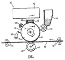
- FIG. 1 shows somewhat schematically a printer 30 incorporating a preferred embodiment of a print cartridge according to the present invention.
- This printer is illustrated primarily to demonstrate a preferred environment for the invention but other printers or charge transfer apparatus could benefit from the use of the invention.
- a cylinder or drum 32 is mounted for rotation about an axis 34 and has an electrically conductive core 35 coated in a dielectric layer 36 capable of receiving a charge image from a print cartridge 38 driven by an electronic control system 40 and connected to the cartridge 38 by electrical connectors 42.
- a charge image is created by the cartridge 38 on the outer surface of the dielectric layer 36 and comes into contact with toner supplied from a hopper 44 by a feed mechanism 46.
- the resulting toner image is carried by the drum 32 towards a nip formed with a pressure roller 48 having a compliant outer layer 49 positioned in the path of a receptor such as a paper sheet 50 which enters between a pair of feed rollers 52.
- the pressure in the nip is sufficient to cause the toner to transfer to the paper sheet 50 and, because the axes of the drum 32 and roller 48 lie at an angle to one another, the toner will be fused to the receptor.
- the paper leaves the printer 30 between a pair of output rollers 54.
- any toner remaining on the surfaces of the dielectric layer 36 is removed by a scraper blade assembly 56, and any residual charge remaining on the surface is neutralized by a discharge head 58 positioned between the scraper blade assembly 56 and the cartridge 38.
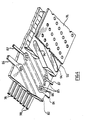
- Fig. 2 is a top view of the print cartridge 38.
- the cartridge is shown as it would appear looking down on the printer of Fig. 1, and has a handle 60 extending beyond the active part of the cartridge for engaging the cartridge in the printer.
- the handle is an extension of a rigid spine 62 of aluminum which extends beyond the cartridge.
- End contacts 66, 67 for driver electrodes can be seen extending to either side of the spine 62 supported by a printed circuit board 70.
- intermediate, elongate finger electrode contacts 71 also extend to either side of the spine, though they are sandwiched between a base member or bottom board 68 (better seen in Fig. 3) and the printed circuit board 70 and are normally only visible through contact apertures in the board 70 for receiving ends of the connectors 42 (Fig. 1).
- the bottom board 68 has a central slot 72 positioned about rows of small apertures 73 in a screen electrode 74.
- the board, or substrate 70 (Fig. 2), is of dielectric material such as glass reinforced epoxy and has printed on its underside a number of driver electrodes or drive lines, indicated collectively by the numeral 78.
- the driver electrodes 78 terminate at positions (not seen) which are connected to inner ends of the contacts 66, and which are parallel to and separated by a strip of dielectric 82, typically mica, from finger electrodes 84.
- Each of these finger electrodes defines groups 85 of individual apertures 86 forming edge structures, and extends from one of the elongate finger electrode contacts 71 to terminate in a support piece 87 for maintaining the finger electrodes in relationship to one another during cartridge manufacture.
- the contacts 71 (Fig. 2) and support pieces 87 are formed integrally with the finger electrodes 84.
- a dielectric separator layer 92 lies between the finger electrodes 84 and the screen electrode 74 and has parallel slots 94 in alignment with the groups of apertures 85 in the finger electrodes where charged particle generation take place.
- each of the groups 85 defines a discharge location and the apertures 86 define individual discharge sites within that location.
- Fig. 4 gives an overview of the arrangement of the various layers in the cartridge 38. Of course, it will be appreciated that layers of adhesive and the like have been omitted for clarity.
- FIG. 5 shows a somewhat schematic view of what would be seen in a sectional view of a prior art cartridge 100 at a location where a driver electrode and a finger electrode intersect.
- an alternating potential from a source 108, is applied between the driver and finger electrodes 110, 112 in combination with bias potentials V1 V2 to create an electrical discharge in apertures such as apertures 114 in the finger electrodes.
- Charged particles formed in the apertures 114 by the discharge are then subjected to an electrical field which causes them to form a charged particle current which is intended to impinge on dielectric layer 106 and form a latent image.
- An additional DC bias potential V2 may be applied to a screen electrode 116 which primarily provides a screening effect on the oppositely charged particles as well as some lensing action on the charged particles in the current.
- Control of the various electrodes to produce a desired image may be achieved by multiplexing, as described, for example, in U.S. Patent No. 4,267,556 issued May 12, 1981 to Fotland et al, or in response to a digital input signal representing successive raster scan lines, as described, for example, in U.S. Patent No. 4,494,129 issued January 15, 1985 to Gretchev.
- the electric field produced by the electrodes penetrates through the apertures 114 and predominates within the cartridge as shown by lines of equipotential 118. Due to the convex shape of this field particles formed in the apertures 114 follow divergent paths, as represented by field lines 120. While the screen electrode 116, where present, may assist in redirecting a portion of the diverging particles, it is clear that only a small proportion of particles will reach the dielectric layer 106 to form an image theron. It can also be seen that a large proportion of the charged particles remain behind the screen 116, where it is thought that the particles contribute to the build up of corona by-products which ultimately affect the performance of the cartridge.
- the provision of a single aperture, and thus a single discharge zone leads to unpredictable and variable image or dot production, due to the uncertainty of discharges occurring during a cycle in the applied alternating potential, and the uncertainty of the location of the origin of the discharge in the aperture.
- FIG. 6 shows a view, similar to FIG 5, of a cartridge configuration which is intended to overcome these problems.
- the cartridge includes a group 85 of apertures 86 in finger electrode 84 at each crossover location of the electrodes 78, 84.
- the electric field created between the driver and finger electrodes 78, 84 as illustrated by lines of equipotential 124, does not extend significantly beyond the dielectric 82, and as a result produces a more homogenous electrical field which causes a straighter charge particle flow 126. Consequently greater number of charged particles are directed towards the dielectric surface 35. Also, because many separate discharges are generated in the group of apertures at each particular location, the reliability and predictability of discharges increases.
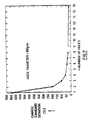
- FIG. 7 shows graphs of standard deviation of emitted charge amount versus number of holes or discharge sites in the finger electrode, during one cycle. It can be seen that the consistency of emitted charge amount increases markedly with increase in hole numbers due to initiation of electrical discharge in a plurality of separate sites leading to an increased statistical probability of discharge.
- SD Standard deviation
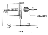
- Fig. 8 represents the experiment conducted to obtain the results used to plot the graph of Fig. 7.
- a single pulse generator was applied between the finger and driving electrodes and the charged particle current was extracted by an external field between the probe and finger electrodes.
- the current circuit was closed by a resistor R which converted the current into a voltage signal. This signal was further recorded by a digital oscilloscope and integrated.
- the background signal (noise and induced voltage) was measured similarly but with zero DC voltage applied between the probe and finger electrodes. Its integral value was extracted from the charge measurements.
- the finger electrodes 84 illustrated in FIGS. 6 and 7 are provided with seven apertures at each location. However, improved results will be obtained by use of any number of apertures, as illustrated by the graph.
- the group 85 of openings may be arranged with a variety of individual openings 86 of differing shapes consistent with enhancing the efficiency of the charge transfer imaging capacity of the structure.
Landscapes
- Physics & Mathematics (AREA)
- General Physics & Mathematics (AREA)
- Printers Or Recording Devices Using Electromagnetic And Radiation Means (AREA)
- Electrophotography Using Other Than Carlson'S Method (AREA)
Applications Claiming Priority (2)
| Application Number | Priority Date | Filing Date | Title |
|---|---|---|---|
| US284267 | 1988-12-14 | ||
| US07/284,267 US4879569A (en) | 1988-12-14 | 1988-12-14 | Multiple source charged particle generation |
Publications (2)
| Publication Number | Publication Date |
|---|---|
| EP0373889A2 true EP0373889A2 (fr) | 1990-06-20 |
| EP0373889A3 EP0373889A3 (fr) | 1990-08-08 |
Family
ID=23089525
Family Applications (1)
| Application Number | Title | Priority Date | Filing Date |
|---|---|---|---|
| EP89312982A Ceased EP0373889A3 (fr) | 1988-12-14 | 1989-12-12 | Source multiple pour la génération des particules chargées |
Country Status (3)
| Country | Link |
|---|---|
| US (1) | US4879569A (fr) |
| EP (1) | EP0373889A3 (fr) |
| JP (1) | JPH02263667A (fr) |
Families Citing this family (5)
| Publication number | Priority date | Publication date | Assignee | Title |
|---|---|---|---|---|
| US5245502A (en) * | 1990-11-23 | 1993-09-14 | Xerox Corporation | Semi-conductor corona generator for production of ions to charge a substrate |
| US5278588A (en) * | 1991-05-17 | 1994-01-11 | Delphax Systems | Electrographic printing device |
| US6028615A (en) * | 1997-05-16 | 2000-02-22 | Sarnoff Corporation | Plasma discharge emitter device and array |
| US7623144B2 (en) * | 2007-01-29 | 2009-11-24 | Hewlett-Packard Development Company, L.P. | Apparatus for electrostatic imaging |
| US8830282B2 (en) * | 2007-06-28 | 2014-09-09 | Hewlett-Packard Development Company, L.P. | Charge spreading structure for charge-emission apparatus |
Family Cites Families (3)
| Publication number | Priority date | Publication date | Assignee | Title |
|---|---|---|---|---|
| CA1209400A (fr) * | 1983-12-09 | 1986-08-12 | Robert S. Mccallum | Cartouche et imprimante ionographiques |
| JPS60196363A (ja) * | 1984-03-19 | 1985-10-04 | Canon Inc | イオン発生装置およびその製造方法 |
| US4697196A (en) * | 1985-02-13 | 1987-09-29 | Canon Kabushiki Kaisha | Electrostatic recording method and apparatus |
-
1988
- 1988-12-14 US US07/284,267 patent/US4879569A/en not_active Expired - Lifetime
-
1989
- 1989-12-12 EP EP89312982A patent/EP0373889A3/fr not_active Ceased
- 1989-12-14 JP JP1324865A patent/JPH02263667A/ja active Pending
Also Published As
| Publication number | Publication date |
|---|---|
| US4879569A (en) | 1989-11-07 |
| JPH02263667A (ja) | 1990-10-26 |
| EP0373889A3 (fr) | 1990-08-08 |
Similar Documents
| Publication | Publication Date | Title |
|---|---|---|
| US4155093A (en) | Method and apparatus for generating charged particles | |
| EP0373888B1 (fr) | Cassette d'impression avec un champ électrostatique non-divergent | |
| US4267556A (en) | Electrostatic transfer printing employing ion emitting print head | |
| US4160257A (en) | Three electrode system in the generation of electrostatic images | |
| US4365549A (en) | Electrostatic transfer printing | |
| EP0752317B1 (fr) | Imprimante de projection de toner avec des moyens pour la réduction de dissémination de toner | |
| US5014076A (en) | Printer with high frequency charge carrier generation | |
| CA1165175A (fr) | Deflecteur de gouttes d'encre | |
| US4879569A (en) | Multiple source charged particle generation | |
| US4544930A (en) | Ink jet printer with secondary, cyclically varying deflection field | |
| JPH0262862B2 (fr) | ||
| US4013004A (en) | Ink mist type high speed printer | |
| US3962969A (en) | Ink mist type high speed printer | |
| US5083145A (en) | Non-arcing blade printer | |
| CA1168294A (fr) | Electrodes de charge a deux sections pour imprimantes binaires a gouttelettes d'encre | |
| WO1987002451A1 (fr) | Imagerie electrostatique par modulation du flux d'ions | |
| US5655184A (en) | Ionographic printing with improved ion source | |
| EP0963852B1 (fr) | Méthode d'impression et contrôle pour une tête d'impression avec électrodes de déviation pour l'impression électrostatique directe | |
| EP0854400A1 (fr) | Système de projection de toner | |
| JP2535973B2 (ja) | イオン流制御記録装置 | |
| JPS63153162A (ja) | 静電記録ヘツド | |
| US6476835B1 (en) | Coplanar thin film printhead | |
| JP2001110547A (ja) | イオン発生器及びそのイオン発生器を備えた静電記録装置 | |
| JP2000118032A (ja) | イオノグラフィ用画像印刷装置 | |
| JPH0764088B2 (ja) | 静電潜像形成装置の駆動方法 |
Legal Events
| Date | Code | Title | Description |
|---|---|---|---|
| PUAI | Public reference made under article 153(3) epc to a published international application that has entered the european phase |
Free format text: ORIGINAL CODE: 0009012 |
|
| AK | Designated contracting states |
Kind code of ref document: A2 Designated state(s): BE CH DE ES FR GB IT LI LU NL SE |
|
| PUAL | Search report despatched |
Free format text: ORIGINAL CODE: 0009013 |
|
| AK | Designated contracting states |
Kind code of ref document: A3 Designated state(s): BE CH DE ES FR GB IT LI LU NL SE |
|
| 17P | Request for examination filed |
Effective date: 19901116 |
|
| 17Q | First examination report despatched |
Effective date: 19920610 |
|
| STAA | Information on the status of an ep patent application or granted ep patent |
Free format text: STATUS: THE APPLICATION HAS BEEN REFUSED |
|
| 18R | Application refused |
Effective date: 19930517 |