EP0374307A1 - Ensemble de connexions pour cartes de circuits imprimés - Google Patents
Ensemble de connexions pour cartes de circuits imprimés Download PDFInfo
- Publication number
- EP0374307A1 EP0374307A1 EP88203014A EP88203014A EP0374307A1 EP 0374307 A1 EP0374307 A1 EP 0374307A1 EP 88203014 A EP88203014 A EP 88203014A EP 88203014 A EP88203014 A EP 88203014A EP 0374307 A1 EP0374307 A1 EP 0374307A1
- Authority
- EP
- European Patent Office
- Prior art keywords
- housing
- contacts
- sidewalls
- additional contacts
- additional
- Prior art date
- Legal status (The legal status is an assumption and is not a legal conclusion. Google has not performed a legal analysis and makes no representation as to the accuracy of the status listed.)
- Granted
Links
- 239000011810 insulating material Substances 0.000 claims abstract description 16
- 239000002184 metal Substances 0.000 claims description 6
- 238000003780 insertion Methods 0.000 description 3
- 230000037431 insertion Effects 0.000 description 3
- 210000002105 tongue Anatomy 0.000 description 3
- 238000010276 construction Methods 0.000 description 2
- 230000002349 favourable effect Effects 0.000 description 2
- 230000002730 additional effect Effects 0.000 description 1
- 230000003247 decreasing effect Effects 0.000 description 1
Images



Classifications
-
- H—ELECTRICITY
- H01—ELECTRIC ELEMENTS
- H01R—ELECTRICALLY-CONDUCTIVE CONNECTIONS; STRUCTURAL ASSOCIATIONS OF A PLURALITY OF MUTUALLY-INSULATED ELECTRICAL CONNECTING ELEMENTS; COUPLING DEVICES; CURRENT COLLECTORS
- H01R12/00—Structural associations of a plurality of mutually-insulated electrical connecting elements, specially adapted for printed circuits, e.g. printed circuit boards [PCB], flat or ribbon cables, or like generally planar structures, e.g. terminal strips, terminal blocks; Coupling devices specially adapted for printed circuits, flat or ribbon cables, or like generally planar structures; Terminals specially adapted for contact with, or insertion into, printed circuits, flat or ribbon cables, or like generally planar structures
- H01R12/70—Coupling devices
- H01R12/7082—Coupling device supported only by cooperation with PCB
-
- H—ELECTRICITY
- H01—ELECTRIC ELEMENTS
- H01R—ELECTRICALLY-CONDUCTIVE CONNECTIONS; STRUCTURAL ASSOCIATIONS OF A PLURALITY OF MUTUALLY-INSULATED ELECTRICAL CONNECTING ELEMENTS; COUPLING DEVICES; CURRENT COLLECTORS
- H01R12/00—Structural associations of a plurality of mutually-insulated electrical connecting elements, specially adapted for printed circuits, e.g. printed circuit boards [PCB], flat or ribbon cables, or like generally planar structures, e.g. terminal strips, terminal blocks; Coupling devices specially adapted for printed circuits, flat or ribbon cables, or like generally planar structures; Terminals specially adapted for contact with, or insertion into, printed circuits, flat or ribbon cables, or like generally planar structures
- H01R12/70—Coupling devices
- H01R12/71—Coupling devices for rigid printing circuits or like structures
- H01R12/72—Coupling devices for rigid printing circuits or like structures coupling with the edge of the rigid printed circuits or like structures
- H01R12/73—Coupling devices for rigid printing circuits or like structures coupling with the edge of the rigid printed circuits or like structures connecting to other rigid printed circuits or like structures
- H01R12/735—Printed circuits including an angle between each other
- H01R12/737—Printed circuits being substantially perpendicular to each other
-
- H—ELECTRICITY
- H01—ELECTRIC ELEMENTS
- H01R—ELECTRICALLY-CONDUCTIVE CONNECTIONS; STRUCTURAL ASSOCIATIONS OF A PLURALITY OF MUTUALLY-INSULATED ELECTRICAL CONNECTING ELEMENTS; COUPLING DEVICES; CURRENT COLLECTORS
- H01R12/00—Structural associations of a plurality of mutually-insulated electrical connecting elements, specially adapted for printed circuits, e.g. printed circuit boards [PCB], flat or ribbon cables, or like generally planar structures, e.g. terminal strips, terminal blocks; Coupling devices specially adapted for printed circuits, flat or ribbon cables, or like generally planar structures; Terminals specially adapted for contact with, or insertion into, printed circuits, flat or ribbon cables, or like generally planar structures
- H01R12/70—Coupling devices
- H01R12/77—Coupling devices for flexible printed circuits, flat or ribbon cables or like structures
- H01R12/81—Coupling devices for flexible printed circuits, flat or ribbon cables or like structures connecting to another cable except for flat or ribbon cable
Definitions
- the invention relates to a connector assembly for printed circuit boards according to the preamble of claim 1 or 9.
- a connector assembly of this type also known as a so-called backplane connector, is described in US patent 4,655,518.
- the first additional contacts are mounted in a sidewall of the first housing and made as a spring type contact.
- the second additional contacts are mounted on one of the outwardly directed sidewalls of the second housing. Therefore, both the first and second additional contacts have to be especially manufactured contacts and have to be fixed in the first and second housing, respectively, in a special manner. These additional contacts are mounted in this special manner to provide current distribution contacts without increasing the dimensions of the connector assembly.
- the connector assembly is characterized by the features of the characterising part of claim 1.
- the first additional contacts can be standard male contacts resulting in the possibility to assemble the first connector element by means of a selective pin insertion machine which inserts all male contacts including the additional contacts at desired locations in the printed circuit board, whereafter the first housing is pushed with its base on the contacts.
- two or more contacts may be connected in parallel on the printed circuit board.
- the pin insertion machine inserts the male contacts only whereas the additional contacts are inserted manually after mounting the first housing.
- Two or more additional contacts can be integral in this case.
- two or more integral additional contacts can be provided with a common power connection end opposite of the contact region of the first housing.
- the first connector element may be preassembled, so that the contacts are inserted in holes of the printed circuit board simultaneously.
- the additional contacts may also be preassembled or may be manually inserted when the connector element is mounted on the printed circuit board.
- the overall dimension of the connector assembly is not increased substantially.
- first additional contacts if due to circumstances one or more of the first additional contacts are damaged, they can be removed easily and replaced by new contacts.
- said first additional contacts extend along a longer distance from said base into said contact region than said male contacts.
- different contact levels can be provided for the contacts so that for example first make/last break facilities for ground and power connections can be provided in a very convenient manner.
- said male contacts and said first additional contacts are lengthened at the side opposite of the contact region of the first housing, a third housing of insulating material being provided including a base and two spaced upright sidewalls extending parallel to each other from said base and defining a second contact region therebetween, said lengthened male and first additional contacts projecting through said base into said second contact region thus providing a third connector element with at least one row of additional contacts close to one of its sidewalls.
- the third connector element may cooperate with a fourth connector element with a fourth housing of insulating material including outwardly directed sidewalls adapted to be fitted between said spaced sidewalls of said third housing, and a plurality of parallel rows of fourth contacts and at least one row of fourth additional contacts, said fourth and fourth additional contacts each having contact portions for contacting the lengthened male and first additional contacts, respectively, when said fourth housing is received between the sidewalls of said third housing, at least one of the outwardly directed sidewalls of said fourth housing being provided with a plurality of slots for receiving said at least one row of lengthened first additional contacts.
- the second and fourth connector elements are identical to each other.
- said fourth connector element is made as a cable connector element for a shielded cable with a plurality of wires connected to said fourth with a metal cap with a passage for said cable adapted to contact the shield of the cable, wherein said at least one row of fourth additional contacts is connected to said metal cap thereby providing a continuous connection from said shield to said first additional contacts.
- said first additional contacts are male contacts mounted in a row in the base of said first housing and said second housing comprises two parts each having outwardly directed sidewalls, one sidewall of one part facing one sidewall of the other part, wherein the printed circuit board to be connected to the contacts of the second housing is to be located above the facing sidewalls, the facing sidewalls of said two parts being provided with slots for receiving said row of first additional contacts, at least one of said parts being provided with said second additional contacts arranged in a row adjacent said sidewall provided with slots.
- This embodiment of the invention may be preferred in high speed applications, as the printed circuit board connected to the contacts of the second housing is located more centrally with respect to the contacts of the second housing, whereby the length of the contacts, in particular the contacts at the outersides of the second housing, can be shorter.
- said parts of said second housing are identical and said row of first additional contacts is mounted in the center of the base of the first housing.
- a connector assembly 1 for connecting a printed circuit board 2 (daughter board) to a printed circuit board 3 (backplane).
- the connector assembly 1 comprises a first connector element 4 connected to the backplane 3 and a second connector element 5 connected to the daughter board 2.
- the first connector element 4 comprises a first housing 6 of insulating material including a base 7 and two spaced upright sidewalls 8 which extend parallel to each other from the base 7. A contact region 9 is defined between sidewalls 8. Further the first connector element 4 is provided with four rows of male signal contacts 10 which are press fit in the backplane 3 and extend through the base 7 into the contact region 9.
- the first connector element 4 is further provided with two rows of first additional contacts 11 and 12 which rows of additional contacts 11, 12 are close to a corresponding sidewall 8.
- the additional contacts 11, 12 are male contacts which are also press fit in the backplane 3 and extend through the base 7 into the contact region 9 of the housing 6 along a longer distance from the base 7 than the signal connector 10.
- a further major advantage of the first connector element 4 is that this connector element can be assembled by a selective pin insertion machine which inserts the signal contacts 10 and additional contacts 11, 12 at the desired locations of the backplane 3 whereafter the housing 6 is pushed with its base 7 on the contacts 10-12.
- the additional contacts 11, 12 can be manually inserted, especially when two or more additional contacts 11, 12 are integral. It is further possible to provide a pre-assembled connector element 4 which is mounted on the backplane 3 by simultaneously inserting all contacts. In this case the additional contacts 11, 12 can also be manually inserted afterwards.
- cross section of the additional contacts 11, 12 may have any desired size and does not have to be equal to the cross section of the male con tacts 10.
- the second connector element 5 is provided with a second housing 13 of insulating material including outwardly directed sidewalls 14 adapted to be fitted between the sidewalls 8 of the first housing 6.
- the second connector element 5 includes four rows of female signal contacts 15 having forked contact portions at their lower ends for contacting the male signal contacts 10 when the second housing 13 is inserted into the first housing 6.
- the forked contact portions of the female contacts 15 lie within cavities 16 of the second housing 13.
- the second connector element 2 is further provided with two rows of second additional contacts 17 and 18 for ground and power connection.
- the rows of additional contacts 17 and 18 are located adjacent a corresponding sidewall 14 of the second housing 13.
- the additional contacts 17, 18 are provided with a spring type tongue 19 as contact portions for contacting the male additional contacts 11, 12.
- the tongues 19 are biased against the sidewalls 14.
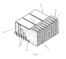
- These sidewalls 14 are further provided with slots 20 as more clearly shown in the perspective view of fig. 2. These slots 20 are provided for receiving the additional contacts 11, 12.
- the overall dimension of the connector assembly is not increased substantially by the provision of the rows of additional contacts.
- the contacts 15, 17 are guided through a guide plate 21 for aligning the outer ends of these contacts with the holes of the daughter board 2 in which the outer ends of all contacts 15, 17 and 19 are for example press fit.
- each three subsequent additional contacts 17 and 18 are integral as shown in fig. 2.
- Fig. 3 shows a second embodiment of a first connector element 22 which mainly corresponds with the first connector element 4 of fig. 1.
- three additional contacts 23 are also integral and provided with a common power connection end 24 as clearly shown in the perspective view of fig. 4.
- the connector element 22 is identical to the connector element 4 and will not further be described. It will be clear that any desired design for power connection to the additional contacts can be chosen.
- the advantage of the use of standard male contacts as additional contacts lies in the fact that in this case they can easily be inserted from the backside of the backplane 3.
- the described design of the first connector element 4 provides the possibility to lengthen the first signal contacts 10 and the additional contacts 11, 12 at the side opposite of the contact region 9 of the first housing 6 as shown in fig. 5.
- a third connector element 25 can be provided with the backplane 3 lying in the center between the connector elements 4 and 25.
- the third connector element 25 comprises a third housing 26 of insulating material with a base 27 and spaced upright sidewalls 28 extending parallel to each other from the base 27. Between the sidewalls 28 a contact region 29 is defined in which the lengthened contacts 8, 11 and 12 are projecting through the base 27. In this manner a high density connection is obtained with the backplane 3 as central heart of the system.
- the third connector element 25 may cooperate with a fourth connector element 30 which is connected to another daughter board 31 and which is identical to the second connector element 5.
- FIG. 6 there is shown an alternative embodiment of the connector assembly with the first connector element 4 and third connector element 25 on both sides of the backplane 3.
- the connector element 25 cooperates with a cable connector element 32 for a shielded cable 33.
- the cable connector element 32 is provided with a metal cap 34 for the cable 33 with a passage for this cable, which passage contacts the shield 35 of the cable 33 as indicated in fig. 6.
- Wires 36 of the cable 33 are connected to the signal contacts 37 mounted in a housing 38 of insulating material.
- the housing 38 mainly corresponds with the housing 13 of the second connector element 5.
- the additional contacts 17, 18 are contacting the metal cap 34 so that a continuous low impedance ground connection from the cable shield 35 to the daughter board 2 is obtained through the additional contacts 11, 12 of the connector elements 25 and 4 and the additional contacts 17, 18 of the connector element 5.
- Fig. 7 and 8 show a first embodiment of the invention in which the length of the contacts is decreased.
- a connector element 39 is provided with a housing 40 of insulating material having two equal parts 41 each having outwardly directed sidewalls 42 and 43.
- the sidewalls 43 of the parts 41 are facing each other and each are provided with slots 44 corresponding with the slots 20 in the sidewall 14 of the housing 13.
- the housing 40 includes four rows of signal contacts 45 with forked contact portions for contacting the male signal contacts 46 of a connector element 47 with a housing 48 of insulating material.
- the construction of the housing 48 corresponds the center of the housing 48, which additional contacts 49 with the construction of the housing 6.
- one row of additional contacts 49 is provided in cooperate with additional contacts 50 of the connector element 39.
- Each part 41 of the housing 40 is provided with one row of additional contacts 50 mounted in the same manner as the additional contacts 17, 18 in the housing 13 of the connector element 5.
- the additional contacts 49 will be received in the slots 44 in the sidewalls 43 of the parts 41 while contacting tongues 51 of the additional contacts 50.
- a daughter board 52 is located in the center of the housing 40 in line with the additional contacts 49 and 50 so that these additional contacts can be provided without increasing the overall dimension of the housing 40.
- the outer ends 53 of all contacts 45 and 50 are surface mounted on the daughter board 52.
- the outer ends of the contacts 45 and 50 of the connector element 39 can also be mounted in plated through holes in the daughter board 52 in any desired manner, for example by press fit.
Landscapes
- Coupling Device And Connection With Printed Circuit (AREA)
- Details Of Connecting Devices For Male And Female Coupling (AREA)
Priority Applications (5)
| Application Number | Priority Date | Filing Date | Title |
|---|---|---|---|
| EP88203014A EP0374307B1 (fr) | 1988-12-23 | 1988-12-23 | Ensemble de connexions pour cartes de circuits imprimés |
| DE3883245T DE3883245T4 (de) | 1988-12-23 | 1988-12-23 | Verbinderanordnung für gedruckte Leiterplatte. |
| AT88203014T ATE93097T1 (de) | 1988-12-23 | 1988-12-23 | Verbinderanordnung fuer gedruckte leiterplatte. |
| ES88203014T ES2045094T3 (es) | 1988-12-23 | 1988-12-23 | Dispositivo conector para paneles de circuitos impresos. |
| DE8888203014A DE3883245D1 (de) | 1988-12-23 | 1988-12-23 | Verbinderanordnung fuer gedruckte leiterplatte. |
Applications Claiming Priority (1)
| Application Number | Priority Date | Filing Date | Title |
|---|---|---|---|
| EP88203014A EP0374307B1 (fr) | 1988-12-23 | 1988-12-23 | Ensemble de connexions pour cartes de circuits imprimés |
Publications (2)
| Publication Number | Publication Date |
|---|---|
| EP0374307A1 true EP0374307A1 (fr) | 1990-06-27 |
| EP0374307B1 EP0374307B1 (fr) | 1993-08-11 |
Family
ID=8199898
Family Applications (1)
| Application Number | Title | Priority Date | Filing Date |
|---|---|---|---|
| EP88203014A Expired - Lifetime EP0374307B1 (fr) | 1988-12-23 | 1988-12-23 | Ensemble de connexions pour cartes de circuits imprimés |
Country Status (4)
| Country | Link |
|---|---|
| EP (1) | EP0374307B1 (fr) |
| AT (1) | ATE93097T1 (fr) |
| DE (2) | DE3883245D1 (fr) |
| ES (1) | ES2045094T3 (fr) |
Cited By (9)
| Publication number | Priority date | Publication date | Assignee | Title |
|---|---|---|---|---|
| EP0545502A1 (fr) * | 1991-12-04 | 1993-06-09 | Framatome Connectors Belgium N.V. | Assemblage de connecteur pour la connexion d'un câble blindé à une plaquette à circuits imprimés |
| EP0627788A1 (fr) * | 1993-06-04 | 1994-12-07 | Framatome Connectors International | Ensemble de connexion |
| US5722861A (en) * | 1996-02-28 | 1998-03-03 | Molex Incorporated | Electrical connector with terminals of varying lengths |
| WO2005093908A1 (fr) * | 2004-02-27 | 2005-10-06 | 3M Innovative Properties Company | Dispositif connecteur |
| US7090501B1 (en) | 2005-03-22 | 2006-08-15 | 3M Innovative Properties Company | Connector apparatus |
| WO2013169552A1 (fr) * | 2012-05-09 | 2013-11-14 | Tyco Electronics Corporation | Système pour l'interconnexion de cartes de circuits imprimés |
| US8851934B2 (en) | 2012-03-20 | 2014-10-07 | Tyco Electronics Corporation | Electrical module housing |
| DE10301474B4 (de) * | 2002-01-17 | 2014-11-27 | Continental Automotive France | Verfahren zum Montieren eines Verbinders |
| CN109524813A (zh) * | 2017-09-20 | 2019-03-26 | 泰科电子(上海)有限公司 | 连接件及电路板组件 |
Citations (3)
| Publication number | Priority date | Publication date | Assignee | Title |
|---|---|---|---|---|
| US4631637A (en) * | 1985-12-23 | 1986-12-23 | Burroughs Corporation | Dual backplane interconnect system |
| GB2185160A (en) * | 1986-01-08 | 1987-07-08 | Teradyne Inc | Daughter board/backplane assembly |
| EP0292144A2 (fr) * | 1987-05-18 | 1988-11-23 | Hirose Electric Co., Ltd. | Connecteur électrique |
-
1988
- 1988-12-23 DE DE8888203014A patent/DE3883245D1/de not_active Expired - Fee Related
- 1988-12-23 AT AT88203014T patent/ATE93097T1/de active
- 1988-12-23 ES ES88203014T patent/ES2045094T3/es not_active Expired - Lifetime
- 1988-12-23 DE DE3883245T patent/DE3883245T4/de not_active Expired - Lifetime
- 1988-12-23 EP EP88203014A patent/EP0374307B1/fr not_active Expired - Lifetime
Patent Citations (3)
| Publication number | Priority date | Publication date | Assignee | Title |
|---|---|---|---|---|
| US4631637A (en) * | 1985-12-23 | 1986-12-23 | Burroughs Corporation | Dual backplane interconnect system |
| GB2185160A (en) * | 1986-01-08 | 1987-07-08 | Teradyne Inc | Daughter board/backplane assembly |
| EP0292144A2 (fr) * | 1987-05-18 | 1988-11-23 | Hirose Electric Co., Ltd. | Connecteur électrique |
Cited By (21)
| Publication number | Priority date | Publication date | Assignee | Title |
|---|---|---|---|---|
| EP0545502A1 (fr) * | 1991-12-04 | 1993-06-09 | Framatome Connectors Belgium N.V. | Assemblage de connecteur pour la connexion d'un câble blindé à une plaquette à circuits imprimés |
| EP0627788A1 (fr) * | 1993-06-04 | 1994-12-07 | Framatome Connectors International | Ensemble de connexion |
| EP0627789A1 (fr) * | 1993-06-04 | 1994-12-07 | Framatome Connectors International | Ensemble de connexion pour cartes de circuits imprimés |
| EP0627790A1 (fr) * | 1993-06-04 | 1994-12-07 | Framatome Connectors International | Ensemble de connexion |
| EP0627791A1 (fr) * | 1993-06-04 | 1994-12-07 | Framatome Connectors International | Ensemble de connexion pour cartes de circuits imprimés |
| NL9300971A (nl) * | 1993-06-04 | 1995-01-02 | Framatome Connectors Belgium | Connectorsamenstel voor printkaarten. |
| US5429521A (en) * | 1993-06-04 | 1995-07-04 | Framatome Connectors International | Connector assembly for printed circuit boards |
| US5433618A (en) * | 1993-06-04 | 1995-07-18 | Framatome Connectors International | Connector assembly |
| US5433617A (en) * | 1993-06-04 | 1995-07-18 | Framatome Connectors International | Connector assembly for printed circuit boards |
| US5549481A (en) * | 1993-06-04 | 1996-08-27 | Framatome Connectors International | Connector assembly for printed circuit boards |
| US5722861A (en) * | 1996-02-28 | 1998-03-03 | Molex Incorporated | Electrical connector with terminals of varying lengths |
| DE10301474B4 (de) * | 2002-01-17 | 2014-11-27 | Continental Automotive France | Verfahren zum Montieren eines Verbinders |
| WO2005093908A1 (fr) * | 2004-02-27 | 2005-10-06 | 3M Innovative Properties Company | Dispositif connecteur |
| US7513797B2 (en) | 2004-02-27 | 2009-04-07 | 3M Innovative Properties Company | Connector apparatus |
| US7722399B2 (en) | 2004-02-27 | 2010-05-25 | 3M Innovative Properties Company | Connector apparatus |
| US7090501B1 (en) | 2005-03-22 | 2006-08-15 | 3M Innovative Properties Company | Connector apparatus |
| US8851934B2 (en) | 2012-03-20 | 2014-10-07 | Tyco Electronics Corporation | Electrical module housing |
| WO2013169552A1 (fr) * | 2012-05-09 | 2013-11-14 | Tyco Electronics Corporation | Système pour l'interconnexion de cartes de circuits imprimés |
| US8721352B2 (en) | 2012-05-09 | 2014-05-13 | Tyco Electronics Corporation | System for interconnecting printed circuit boards |
| CN104303369A (zh) * | 2012-05-09 | 2015-01-21 | 泰科电子公司 | 用于互连印刷电路板的系统 |
| CN109524813A (zh) * | 2017-09-20 | 2019-03-26 | 泰科电子(上海)有限公司 | 连接件及电路板组件 |
Also Published As
| Publication number | Publication date |
|---|---|
| DE3883245D1 (de) | 1993-09-16 |
| DE3883245T2 (de) | 1994-01-27 |
| ES2045094T3 (es) | 1994-01-16 |
| ATE93097T1 (de) | 1993-08-15 |
| DE3883245T4 (de) | 1994-05-26 |
| EP0374307B1 (fr) | 1993-08-11 |
Similar Documents
| Publication | Publication Date | Title |
|---|---|---|
| EP0670616B1 (fr) | Connecteur pour un câble pour signaux hautes fréquences | |
| EP0555963B1 (fr) | Connecteur avec bus de mise à la terre en une seule pièce | |
| US6435913B1 (en) | Header connector having two shields therein | |
| EP0620616B1 (fr) | Connecteur pour câble coaxial et/ou câble biaxial | |
| US6293827B1 (en) | Differential signal electrical connector | |
| US5037334A (en) | Connector with equal lateral force contact spacer plate | |
| EP0674364A1 (fr) | Connecteur de type jack modulaire | |
| EP0337659A1 (fr) | Système de retenue de broches de brasage | |
| US5993263A (en) | Reduced mating force electrical connector | |
| EP0156539A1 (fr) | Dispositif de clef et mise en oeuvre de ce dispositif pour connecteurs électriques | |
| US5281165A (en) | Electrical connector shroud adapted for shorting bar removal | |
| US6648657B1 (en) | Electrical connector having ground buses | |
| KR0121794Y1 (ko) | 분로식 전기 커넥터 | |
| EP0740372B1 (fr) | Connecteur électrique | |
| EP0365179B1 (fr) | Système de connecteur électrique | |
| EP0374307A1 (fr) | Ensemble de connexions pour cartes de circuits imprimés | |
| US5071372A (en) | Connector with contact spacer plate having tapered channels | |
| US6123584A (en) | Connector | |
| US4752246A (en) | Preloaded spring contact electrical terminal | |
| EP0551082B1 (fr) | Ensemble circuit imprimé/dispositif de connexion de bord à stabilisation, procédé pour son assemblage ainsi que connecteur pour le reçevoir | |
| EP1263087B1 (fr) | Bloc à bornes et connecteur pour câbles | |
| EP0891018B1 (fr) | Connecteur | |
| US6159048A (en) | Connector for high frequency signals | |
| EP0969566A1 (fr) | Connecteur et procédé de fabrication d'un connecteur | |
| US5921784A (en) | High speed card edge connector with tubular shared ground contact |
Legal Events
| Date | Code | Title | Description |
|---|---|---|---|
| PUAI | Public reference made under article 153(3) epc to a published international application that has entered the european phase |
Free format text: ORIGINAL CODE: 0009012 |
|
| 17P | Request for examination filed |
Effective date: 19890929 |
|
| AK | Designated contracting states |
Kind code of ref document: A1 Designated state(s): AT BE CH DE ES FR GB GR IT LI LU NL SE |
|
| 17Q | First examination report despatched |
Effective date: 19910218 |
|
| RAP1 | Party data changed (applicant data changed or rights of an application transferred) |
Owner name: FRAMATOME CONNECTORS BELGIUM N.V. |
|
| GRAA | (expected) grant |
Free format text: ORIGINAL CODE: 0009210 |
|
| AK | Designated contracting states |
Kind code of ref document: B1 Designated state(s): AT BE CH DE ES FR GB GR IT LI LU NL SE |
|
| REF | Corresponds to: |
Ref document number: 93097 Country of ref document: AT Date of ref document: 19930815 Kind code of ref document: T |
|
| REF | Corresponds to: |
Ref document number: 3883245 Country of ref document: DE Date of ref document: 19930916 |
|
| ITF | It: translation for a ep patent filed | ||
| K2C2 | Correction of patent specification (partial reprint) published |
Effective date: 19930811 |
|
| ET | Fr: translation filed | ||
| PGFP | Annual fee paid to national office [announced via postgrant information from national office to epo] |
Ref country code: GR Payment date: 19931227 Year of fee payment: 6 |
|
| PGFP | Annual fee paid to national office [announced via postgrant information from national office to epo] |
Ref country code: AT Payment date: 19931230 Year of fee payment: 6 |
|
| REG | Reference to a national code |
Ref country code: ES Ref legal event code: FG2A Ref document number: 2045094 Country of ref document: ES Kind code of ref document: T3 |
|
| PGFP | Annual fee paid to national office [announced via postgrant information from national office to epo] |
Ref country code: LU Payment date: 19940131 Year of fee payment: 6 |
|
| REG | Reference to a national code |
Ref country code: GR Ref legal event code: FG4A Free format text: 3009669 |
|
| EPTA | Lu: last paid annual fee | ||
| PLBE | No opposition filed within time limit |
Free format text: ORIGINAL CODE: 0009261 |
|
| STAA | Information on the status of an ep patent application or granted ep patent |
Free format text: STATUS: NO OPPOSITION FILED WITHIN TIME LIMIT |
|
| 26N | No opposition filed | ||
| PGFP | Annual fee paid to national office [announced via postgrant information from national office to epo] |
Ref country code: GB Payment date: 19941124 Year of fee payment: 7 |
|
| PGFP | Annual fee paid to national office [announced via postgrant information from national office to epo] |
Ref country code: FR Payment date: 19941129 Year of fee payment: 7 |
|
| PGFP | Annual fee paid to national office [announced via postgrant information from national office to epo] |
Ref country code: CH Payment date: 19941202 Year of fee payment: 7 |
|
| PGFP | Annual fee paid to national office [announced via postgrant information from national office to epo] |
Ref country code: ES Payment date: 19941212 Year of fee payment: 7 |
|
| PGFP | Annual fee paid to national office [announced via postgrant information from national office to epo] |
Ref country code: BE Payment date: 19941214 Year of fee payment: 7 |
|
| PGFP | Annual fee paid to national office [announced via postgrant information from national office to epo] |
Ref country code: SE Payment date: 19941216 Year of fee payment: 7 |
|
| PG25 | Lapsed in a contracting state [announced via postgrant information from national office to epo] |
Ref country code: LU Free format text: LAPSE BECAUSE OF NON-PAYMENT OF DUE FEES Effective date: 19941223 Ref country code: AT Effective date: 19941223 |
|
| PGFP | Annual fee paid to national office [announced via postgrant information from national office to epo] |
Ref country code: NL Payment date: 19941231 Year of fee payment: 7 |
|
| EAL | Se: european patent in force in sweden |
Ref document number: 88203014.1 |
|
| PGFP | Annual fee paid to national office [announced via postgrant information from national office to epo] |
Ref country code: DE Payment date: 19950227 Year of fee payment: 7 |
|
| PG25 | Lapsed in a contracting state [announced via postgrant information from national office to epo] |
Ref country code: GR Free format text: THE PATENT HAS BEEN ANNULLED BY A DECISION OF A NATIONAL AUTHORITY Effective date: 19950630 |
|
| REG | Reference to a national code |
Ref country code: GR Ref legal event code: MM2A Free format text: 3009669 |
|
| PG25 | Lapsed in a contracting state [announced via postgrant information from national office to epo] |
Ref country code: GB Effective date: 19951223 |
|
| PG25 | Lapsed in a contracting state [announced via postgrant information from national office to epo] |
Ref country code: SE Effective date: 19951224 |
|
| PG25 | Lapsed in a contracting state [announced via postgrant information from national office to epo] |
Ref country code: LI Effective date: 19951231 Ref country code: CH Effective date: 19951231 Ref country code: BE Effective date: 19951231 |
|
| BERE | Be: lapsed |
Owner name: FRAMATOME CONNECTORS BELGIUM N.V. Effective date: 19951231 |
|
| PG25 | Lapsed in a contracting state [announced via postgrant information from national office to epo] |
Ref country code: NL Effective date: 19960701 |
|
| GBPC | Gb: european patent ceased through non-payment of renewal fee |
Effective date: 19951223 |
|
| REG | Reference to a national code |
Ref country code: CH Ref legal event code: PL |
|
| PG25 | Lapsed in a contracting state [announced via postgrant information from national office to epo] |
Ref country code: FR Effective date: 19960830 |
|
| NLV4 | Nl: lapsed or anulled due to non-payment of the annual fee |
Effective date: 19960701 |
|
| PG25 | Lapsed in a contracting state [announced via postgrant information from national office to epo] |
Ref country code: DE Effective date: 19960903 |
|
| REG | Reference to a national code |
Ref country code: FR Ref legal event code: ST |
|
| PG25 | Lapsed in a contracting state [announced via postgrant information from national office to epo] |
Ref country code: ES Free format text: LAPSE BECAUSE OF NON-PAYMENT OF DUE FEES Effective date: 19961224 |
|
| REG | Reference to a national code |
Ref country code: ES Ref legal event code: FD2A Effective date: 19970113 |
|
| PG25 | Lapsed in a contracting state [announced via postgrant information from national office to epo] |
Ref country code: IT Free format text: LAPSE BECAUSE OF NON-PAYMENT OF DUE FEES;WARNING: LAPSES OF ITALIAN PATENTS WITH EFFECTIVE DATE BEFORE 2007 MAY HAVE OCCURRED AT ANY TIME BEFORE 2007. THE CORRECT EFFECTIVE DATE MAY BE DIFFERENT FROM THE ONE RECORDED. Effective date: 20051223 |