EP0374526A2 - OP-Verzweigung zum Starten von Mikroroutinen - Google Patents
OP-Verzweigung zum Starten von Mikroroutinen Download PDFInfo
- Publication number
- EP0374526A2 EP0374526A2 EP89121760A EP89121760A EP0374526A2 EP 0374526 A2 EP0374526 A2 EP 0374526A2 EP 89121760 A EP89121760 A EP 89121760A EP 89121760 A EP89121760 A EP 89121760A EP 0374526 A2 EP0374526 A2 EP 0374526A2
- Authority
- EP
- European Patent Office
- Prior art keywords
- microprogram
- macroinstruction
- instruction
- code
- processor
- Prior art date
- Legal status (The legal status is an assumption and is not a legal conclusion. Google has not performed a legal analysis and makes no representation as to the accuracy of the status listed.)
- Withdrawn
Links
Images


Classifications
-
- G—PHYSICS
- G06—COMPUTING OR CALCULATING; COUNTING
- G06F—ELECTRIC DIGITAL DATA PROCESSING
- G06F9/00—Arrangements for program control, e.g. control units
- G06F9/06—Arrangements for program control, e.g. control units using stored programs, i.e. using an internal store of processing equipment to receive or retain programs
- G06F9/30—Arrangements for executing machine instructions, e.g. instruction decode
- G06F9/30181—Instruction operation extension or modification
- G06F9/30189—Instruction operation extension or modification according to execution mode, e.g. mode flag
-
- G—PHYSICS
- G06—COMPUTING OR CALCULATING; COUNTING
- G06F—ELECTRIC DIGITAL DATA PROCESSING
- G06F9/00—Arrangements for program control, e.g. control units
- G06F9/06—Arrangements for program control, e.g. control units using stored programs, i.e. using an internal store of processing equipment to receive or retain programs
- G06F9/22—Microcontrol or microprogram arrangements
- G06F9/26—Address formation of the next micro-instruction ; Microprogram storage or retrieval arrangements
- G06F9/262—Arrangements for next microinstruction selection
- G06F9/268—Microinstruction selection not based on processing results, e.g. interrupt, patch, first cycle store, diagnostic programs
-
- G—PHYSICS
- G06—COMPUTING OR CALCULATING; COUNTING
- G06F—ELECTRIC DIGITAL DATA PROCESSING
- G06F9/00—Arrangements for program control, e.g. control units
- G06F9/06—Arrangements for program control, e.g. control units using stored programs, i.e. using an internal store of processing equipment to receive or retain programs
- G06F9/30—Arrangements for executing machine instructions, e.g. instruction decode
- G06F9/30145—Instruction analysis, e.g. decoding, instruction word fields
Definitions
- This invention relates to digital computers. More specifically, the present invention relates to a mechanism in a microprogrammed computer for translating a macroinstruction into its associated microinstruction routines.
- LSI microprocessor design has reached the stage where new implementation techniques are required in order to control cost and increase life and flexibility.
- One technique for achieving these goals is to microprogram the instruction set used in controlling the processor. Microprogramming traditionally claims benefits of regularity (to decrease complexity), flexibility (to ease design changes), and reduced design cost.
- a processor performs a series of operations upon digital information in an execution unit according to a stored program of instructions. These instructions are often termed "macroinstructions" in order to avoid confusion with the microinstructions contained in the control store of the processor.
- the microinstructions are often grouped into microinstruction routines in order to perform various macroinstructions.
- the grouped microinstruction routines constitute the microprogram of the processor.
- Prior art processors use microprogrammed instructions to control internal circuitry in response to macroinstructions. These processors use table look-up approaches to map a macroinstruction into the appropriate microinstruction routines/microprogram.
- One prior art approach uses control store table entries consisting of microinstruction routines and blocks of micro-branches. The targets of the micro-branches are the first microinstruction of the microinstruction routines/microprogram. Each micro-branch is accessed by an address formed directly from the operation-code (op-code) of the macroinstruction.
- the micro-branch entries are physically remote from the processor in firmware, a ROM, to permit flexibility during the manufacturing process.
- Another prior art processor uses microprogrammed storage divided into three sections. It is possible to execute macroinstructions of another processor using the three section memory to control the internal circuitry of the processor.
- One problem with this approach is the requirement of a multi-section memory which adds cost and complexity.
- Another drawback is that the processor is not capable of executing the same macroinstruction by either hardware or microprogram.
- a processor accesses operation-code break out storage which has at least one instruction resolution table embedded in Random-Access-Memory (RAM).
- the table contains entries representing origins of various microinstruction routines.
- the table entries are accessible by the processor and are written during processor initialization. Specific bits of the macroinstruction operation-code are used to access the table entries.
- the contents of the table entry are assembled at the output of the resolution table and are used to address the first microinstruction of microinstruction routines/microprogram in a single level control storage array. Expansion of the number of macroinstructions capable of execution by the processor is achieved by adding additional resolution tables.
- Hardware setup of the macroinstruction information is in a single convenient facility, which is also accessible by the microinstructions, permitting hardware assembly of data and eliminating operations normally required through the execution of additional microinstructions.
- the invention provides a method of translating a macroinstruction into an associated micro-program routine where the instruction set consists of hardware executed instructions and microprogrammed instructions.
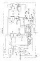
- Fig. 2 is a representation of a typical system which contains a processor and memory packaged on a single card, called the Processor Unit 500 or PU card.
- the Instruction Processing Unit (IPU) 10, Data Cache Unit (DCU) 70, Instruction Cache Unit (ICU) 80, L1 Memory Management Control (TLB) 60, Control Store Unit (CSU) 30, and Floating Point Unit (FPU) 50 all reside on the same card.
- Each of the units is packaged on a se parate Multiple Chip Ceramic Modules (MCMs) with a maximum of four chips per Multiple Chip Ceramic Module.
- MCMs Multiple Chip Ceramic Modules
- the units are interconnected by a number of data and control busses.
- the Storage Bus (STG-BUS) 110 is a bidirectional data/control interface between the Instruction Cache Unit 80, Control Store Unit 30, Data Cache Unit 70 and Memory Management Unit 60. In addition, this bus extends off the Processor Unit card to interface with main memory which is packaged on a separate card. Three bidirectional data busses, Cache Addressing Unit Bus (CAU DBus) 108, Floating Point Unit Data Bus (FPU DBus) 107, Instruction Processor Unit Data Bus 109 (IPU DBus) connect the Data Cache Unit 70 with the Memory Management Unit 60, the Floating Point Unit 50 and the Instruction Processor Unit 10, respectively.
- the Memory Management Unit 60 operates to provide communications between all of the units on the Processor Unit card.
- the Data Cache Unit 70 performs storage data fetches and stores.
- the Data Cache Unit 70 serves as a central data switch between the Instruction Processor Unit 10, Memory Management Unit 60 and the Floating Point Unit 50.
- the Command Bus (CBus) 106 is driven by the Instruction Processor Unit 10 and informs the other four units of requests to do operations initiated by the macroinstruction or microinstruction stream.
- the Command Bus 106 serves as a means for communicating to the other four units certain interrupting conditions (e.g., main memory commands to TLB/DCU/ICU); Input/Output actions, and any maintenance actions from outside the Processor Unit boundary.
- the Effective Address (EA) 105 Bus conveys operand and instruction addresses to the Memory Management Unit 60, Data Cache Unit 70 and Instruction Cache Unit 80.
- the Instruction Bus (IBus) 101 is a tri-state bus over which either the Instruction Cache Unit 80 or Control Store Unit 30 can drive instructions or microword to the Instruction Processor Unit 10.
- the Control Store Origin Address Bus 103 (CSOA) delivers new microwords stream control store addresses from the Instruction Processor Unit 10 to the Control Store Unit 30.
- the Control Store Origin Address Bus 103 exchanges control store addresses and controls between the two units for micro-branch and links (micro subroutine provisions).
- Boundary latches required for interunit communications have resulted in delays requiring a full cycle.
- bus transfers and control interface transitions require a full cycle for some intraunit activity.
- dead time is the initial start-up of the micro-program from a macroinstruction.
- the initial micro-program start-up period is the time between the End-Operation (Endop) of the previous instruction and the decode cycle of the first microword of the next instruction's microprogram.
- S/370 System/370
- the Instruction Processor Unit 10 pipeline is viewed to begin with the decode cycle.
- the decode cycle triggers all subsequent pipelined states and operations. Preceding the decode cycle is the Instruction Bus 101 cycle (IBus) with either an Instruction-Valid (IVALID) or Control-Store-Valid (CSVALID) indication.
- IBus Instruction Bus 101 cycle
- CSVALID Control-Store-Valid
- the IPU 10 will not act on any decode cycles of instructions or microwords that are not preceded by one of these signals.
- the decode cycle of a macroinstruction begins the Operation-Code Break Out (OPBR) Process.
- OPBR Operation-Code Break Out
- the first cycle of the OPBR process consists of: 1) determining whether to perform the macroinstruction in hardware or by microprogram execution, 2) creating the origin address of the microprogram in the Control Store Unit 10, and appropriating hardware entities to setup or "assist in carrying out" the macroinstruction if it is to be done by microprogram.
- the macroinstruction is decoded to detect all operation-codes that are microprogrammed instructions.
- Hardware controlled entities such as program-status-words (PSW), Control Register (CR) bits and Extended Architecture mode (XA) bits are combined with other decodes to conditionally microprogram certain macroinstructions or to add versatility to the Control Store Origin Address (CSOA) generation.
- PSW program-status-words
- CR Control Register
- XA Extended Architecture mode
- the local primary CSOA resolution table 41 is implemented using embedded Random Access Memory (RAM).
- the local primary table will be referred to as the Main OPBR table.
- the table is physically part of the IPU 10 logic shown in Fig. 2.
- the entries in this main table are addressed by using the Operation-Code (Op-code) of the System/370 (S/370) macroinstruction.
- the entries in the main table consist of four logical fields. The logical fields are:
- Additional resolution tables may be added to increase the number of microprogrammed instructions.
- the additional tables are designated Detail Resolution Tables 43 (DT) and any number may be added per the user's requirement, in addition, to the Main OPBR 41 table.
- the entries in the DT array 43 have the following format:
- the S/370 Complex Instruction Set Computer has an instruction set composed of general and extended operation-code group instructions.
- the extended Op-code group instruction consists of complex control instructions, operating system assist instructions and Vector Processor instructions.
- the extended operation-code of the instructions in each group is used to address the entries in the resolution tables 41, 43.
- the first eight instruction bits of instructions in either group are designated the normal Op-code. Therefore, in normal operation, 256 possible entries can be addressed in the resolution table, representing 256 different instructions.
- extended Op-code instructions have eight additional bits. Thus, the first 16 bits of extended Op-code instructions are available for addressing resolution tables.
- the normal part of the Op-code is used to select the corresponding DT.
- loading the contents of the selected DT 43 into a staging register will prohibit the loading of any other DT outputs or the Main OPBR table 41 output into the same staging register.
- the eight resolution tables 41, 43 are all implemented in RAM and are alterable by maintenance activities. These maintenance activities are part of a maintenance subsystem included in the Processor's total logic.
- the maintenance subsystem consists of logic and microprograms which perform functions associated with such things as diagnostics, initialization of hardware and overall machine serviceability.
- the Instruction Processor Unit 10 is shown connected to its corresponding cache. It should be noted that the Instruction Processor Unit 10 may be termed the “Processor” or “Instruction/Execution Unit”, but for the sake of simplicity in the description below, the block will be called the Instruction Processor Unit 10. In addition, the Instruction Cache Unit 80 and the Data Cache Unit 70 can be called the cache.
- the Control Store Unit 30 comprises a high speed fixed control store 35, a pageable area 36, a directory for the pageable Control Store 37, a Control Store Address Register (CSAR) 39, and a Branch and Link (BAL STK) facility 38.
- ACR Control Store Address Register
- BAL STK Branch and Link
- Machine state controls include the global controls 31 for the Processor, an OP-branch break out table 33 connected to the Control Store Address Register 39 via the Control Store Origin Address 103 Bus and used to generate the initial address for microcoded instructions.
- the address generation unit consists of an Instruction Cache DLAT and directory 25, a Data Cache DLAT and directory 23, and an address generation chip 24 connected to the cache via the address bus 105.
- the instruction DLAT 25 is connected to the Instruction Cache 84 portion of the cache via four "hit" lines which indicate that the requested instruction will be found in the instruction cache portion of the cache. Likewise, four "hit” lines connect the data DLAT 23 and directory indicating that the requested data will be found in the Data Cache portion 76 of the cache.
- the address generation unit 24 contains copies of the General Purpose Registers used to generate addresses and includes three storage address registers (SARs) 26, used to provide addresses to the microcode for instruction execution.
- the Instruction Processor Unit 10 is connected to the Data Cache Unit 70 and contains a Local Store array 15 which contains the General Purpose Registers (GPR) mentioned above and a number of working registers used exclusively by the micro-code.
- GPR General Purpose Registers
- Condition registers 14 contain the results of a number of arithmetic and shift type operations and contain the results of a S/370 condition code; an Arithmetic Logic Unit (ALU) 17; a Rotate Merge Unit 16; Branch Bit Select hardware 13 which allows the selection of bits from various registers which determine the direction of a branch operation, the bits being selected from General Purpose Registers 15, Working registers, and the Condition Registers.
- a Floating Point Processor 50 includes floating point registers and four microcode working registers 51, a command decode and control function 52, a floating point adder 53, a fixed point and floating point multiply array 54, and a square-root and divide facility 55. The Floating Point Processor 50 is disclosed in pending patent application Serial No.
- the ALU 17 contains an adder, the adder being disclosed in pending patent application Serial No. 066,580, filed June 26, 1987, entitled “A High Performance Parallel Binary Byte Adder", the disclosure of which is incorporated by reference into the specification of this application.
- An externals chip 90 includes timers and interrupt structure, the interrupts being provided from the I/O subsystem 14, and others.
- the cache comprises the following elements: an Instruction Cache 84, an instruction buffer 82 at the output thereof, and an inpage register 86 connected to the CSU 30.
- the storage bus 110 is connected to the instruction cache unit 80, being connected to the inpage register 86.
- the inpage register 86 is connected to the control store unit 30 and provides data to the unit in the event of a pageable control store miss and new data must be brought into the control store 30.
- the data cache 70 comprises an inpage buffer 78 also connected to the storage bus 110; a data cache 76; a cache dataflow 72 which comprises a series of input and output registers and which is connected to the Instruction Processor Unit 10; and store buffer (STOR BFR) 74.
- the first operation describes a pure hardware execution of a macroinstruction. This operation may also be referred to as "hardwired" or hardware macroinstruction execution mode.
- a macroinstruction to be executed is located in the instruction cache 84.
- the instruction is fetched from the instruction cache 84 and is stored in the instruction buffer 82 (every attempt is made to keep the instruction buffer full at all times).
- the instruction is fetched from the instruction buffer 82 and is stored in the instruction registers of the address generation chip 20, the ALU 17 and Rotate Merge Chip 16, and the machine state controls 32, at which point, the instruction decoding begins.
- Operands are fetched from the GPR COPY 22 in the address generation unit 24 if an operand is required (normally, GPR COPY is accessed if operands are required for the base and index registers for an RX instruction). In the next cycle, the address generation process begins.
- the base and index register contents are added to a displacement field of the instruction, and the effective address is generated and sent to the data cache 70 and/or the instruction cache 80.
- an operand is sought. Therefore, the effective address will be sent to the Data Cache 70.
- the address is also sent to the data DLAT and directory chip 23 (since, in this example, an operand is sought). Access to the cache and the directories will begin in the third cycle.
- the DLAT 23 will determine if the address is translatable from an effective address to an absolute address. Assuming that this translation has been previously performed, we will have recorded the translation.
- the translated address is compared with the output of the cache directory 23.
- the directory output and the DLAT output are compared; if they compare equal, one of the four "hit" lines are generated from the data DLAT and directory 23.
- the hit lines are connected to the Data Cache 76; a generated "hit” line will indicate which of the four associativity classes contains the data that we wish to retrieve.
- the data cache 76 output is gated through a fetch alignment shifter in the cache dataflow 72. The data is transmitted to the IPU 10, and is latched into the ALU 17. This will be the access of operand 2 of an RX type of instruction. In parallel with this shifting process, operand 1 is accessed from the General Purpose Registers in Local Store 15.
- the ALU 17 will process (add, subtract, divide, etc.) the two operands accordingly, as dictated by the macroinstruction's op-code.
- the output of the ALU 17 is latched and the condition registers 14 are latched, at the end of the fifth cycle, to indicate an overflow or zero condition.
- the output of the ALU 17 is written back into the local store 15 and into the GPR copy 22 of the address generation unit 24 in order to keep the GPR copy 22 in sync with the content of the local store 15.
- the decode cycle of this instruction may begin, so that there will be up to six macroinstructions in either decoding or execution at any one time.
- Figs. 2-4 an operation will now be described for a macroinstruction executed using microprogramming.
- the OP-branch table 33 is searched, using the Op-code from the instruction as an address, the OP-branch table 33 provides the beginning address of the microinstruction routines needed to execute the instruction.
- Cycle 1 of the IPU 10 pipeline is viewed to begin with the decode cycle which triggers all subsequent pipeline states and operations.
- the decoded bits of the macroinstruction are modified with architecture control entries such as the PSW, XA Mode bit, and CR bits before they are driven to the resolution tables. Turning briefly to Fig. 4, the decoded bits are driven to the resolution tables 41, 43. Selection and multiplexing of one of the CSA's, ALTCSA or one of four variations of DT1-DT7 results in a final Control Store Origin Address (CSOA).
- CSOA Control Store Origin Address
- the output of the Main Table 41 or one of DT1-DT7 43 is latched into a staging register, called the OPBR register 45 in Fig. 4.
- the LSAC for the current instructions is also latched at the output of the Main Table 41 into the OPBR LSAC 53 register.
- the Main Table LSAC is used for every OPBR, even during extended Op-code instructions when the Main table's ALTCSA/CSA fields are not used.
- macroinstructions executed using microprogramming require more than one cycle to execute. Therefore, instruction decoding is suspended while the OP-branch table is being accessed.
- the IBUS 101 is utilized to provide microinstructions to the decoding hardware.
- the instruction cache 84 is shut-off, the control store 35 is turned-on, and the microinstructions are passed over the IBUS.
- Floating Point Instructions For Floating Point Instructions, decoding proceeds as previously described, except that, during the address generation cycle, a command is sent to the Floating Point Unit 50 to indicate and identify the proper operation to perform.
- an operand is fetched from the Data Cache 76, as described above, and the operand is transmitted to the Floating Point Processor 50 in lieu of the IPU 10.
- Execution of the Floating Point Instruction is commenced. When complete, the results of the execution are returned to the IPU 10, the "results" being condition code, and any interrupt conditions, such as overflow.
- Cycle 2 the contents of the OPBR register 45 are multiplexed onto the CSOA 103 Bus.
- the CSU 30 receives the contents of the CSOA bus and latches it into the CSAR 39 register.
- Cycle 2 is completed in the IPU 10 by loading the IPU's copy of the CSAR from the OPBR 45 register and then loading bits 12-17 of the OPBR 45 register from the OPBR LSAC 53 register.
- Cycle 3 is occupied by two main activities and represents the end of the OPBR process.
- the first activity occurs in the CSU 30 where the contents of the CSAR 39 are used to access the CS array 35.
- the microinstruction stored at the accessed location is assembled from bit-sliced portions across 6 CS chips, and is sent to the IPU 10.
- the second activity consists of a concurrent operation in the IPU 10, where the IPU 10 sends the OPBR LSAC 53 contents latched in the OPBR register 45 to the CSU 30 over the CSOA 103 bus. This operation ends the OPBR process and the PU card 10 is now in normal micromode. In normal micromode, the CSU 30 can perform one of two possible operations.
- the first may consist of accessing and driving a microinstruction while latching the incremented CSAR 39 that points to the next sequential microinstruction.
- the second operation may be a response to one of the interface commands, such as "hold”, “branch”, or "return".
- the PU remains in micromode until an Endop microinstruction is encountered.
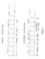
- Cycle 4 begins the decode of the first microword in the microprogram. Since the micro-architecture is a reduced instruction set (RIS) type, the execution of each microword resembles either RR type, load type, or store type instructions of the S/370 architecture. Each of these microwords is executed in three to four cycles (stages) with the decode of the microword as cycle one of the microword. Depending on the microword in execution, cycle two of the microword is used to generate storage address and storage request in the case of load or store microword, or cycle two is the execution cycle in the case of RR microword.
- RIS reduced instruction set
- Cycle three of the microword is the MMU 60/Data Cache Unit 70 access in the case of the load or store type or the GPR 22/LS 15 updates with the temporary (WRT the macroinstruction) execution result in the case of the RR type.
- the microprogram execution is preformed in a pipeline fashion with the start of a new microword in every cycle. This pipeline execution continues until the decode of the last microinstruction or Endop in the microprogram.
- HW MODE Hardware Mode
- USE AIR Use Alternate Instruction Register
- Degate CSU/ICU signal Degate CSU/ICU signal.
- the HW MODE governs the interpretation of the effective instruction.
- the HW MODE signal also operates to perform a different function during processor setup or initialization.
- a FIFO stack is maintained for HW MODE states for handling responses from other units and interrupts resulting from execution of microinstructions in a deep pipeline processor.
- HW MODE is set when a microinstruction routine is completed by the decode or execution of an Endop microword.
- the IPU 10 contains two registers, IR 11 and AIR 20, which latches macroinstructions and microinstructions.
- the decodes of these registers signify and enable the beginning of processor execution.
- the outputs of the two registers are exclusively multiplexed to provide a single set of instruction information/data to the IPU logic.
- This signal also serves the performance function of keeping the instruction that follows a microcoded instruction saved in the IPU 10 when in micromode.
- the latched USE AIR signal is applied to hold the present value of IR 11 such that the last instruction sent by ICU 80, which is the next sequential instruction, is captured. This permits the IPU 10 to decode the next instruction directly after executing the Endop microword cycle. To perform this function, USE AIR must be activated during the decode cycle of the microcoded instruction while the next sequential instruction is driven on the IBus 101. This requirement may be met by providing any two registers and need not be dedicated full time instruction registers. Without this provision, every microcoded instruction would incur 1 to 3 dead cycles in the IPU 10, since the ICU 80 would have to redrive the next instruction.
- a third significant control is the Degate ICU/CSU signals.
- the output of latched Degate ICU is used by ICU 80 in its active state to disable its IBus 101 and place the drivers in a high impedance state. Conversely, the opposite level of the signal enables ICU 80 to drive the bus.
- the signal causes ICU 80 to hold the current instruction thus allowing the ICU 80 to send the second macroinstruction after the prior macroinstruction when the microinstruction routine is finished and the signal is released.
- Degate CSU is used the same way in the CSU 30. The two signals are mutually exclusive and if simultaneously driven causes both ICU 80 and CSU 30 to both drive the IBus 101 with possible catastrophic results.
- IPU 10 setup functions are performed in hardware eliminating the need for additional microcode.
- accessing a facility without saving or accessing and saving the latter is preferred.
- This invention assembles all the items needed for a microprogram into an easily accessible register set at the beginning of the microprogram. This is all done in hardware thus eliminating the need for extra microcode to preform the function.
- SARs Storage Address Registers 26
- LENs which give the length in bytes of the associated data/locations in storage for the operand used in storage to storage instructions
- GR General Register
- LEXT a multitude of system and architectural status and control parameters, organized into a local external mapping and access schemes.
- the process of establishing the proper values for each item occurs during Instruction setup. The values are held after being established by switching the HW MODE to zero. After being set, the values are available for direct and implicit access by certain microwords, including alteration as a result of a microword.
Landscapes
- Engineering & Computer Science (AREA)
- Software Systems (AREA)
- Theoretical Computer Science (AREA)
- Physics & Mathematics (AREA)
- General Engineering & Computer Science (AREA)
- General Physics & Mathematics (AREA)
- Advance Control (AREA)
- Executing Machine-Instructions (AREA)
Applications Claiming Priority (2)
| Application Number | Priority Date | Filing Date | Title |
|---|---|---|---|
| US28743088A | 1988-12-21 | 1988-12-21 | |
| US287430 | 1988-12-21 |
Publications (2)
| Publication Number | Publication Date |
|---|---|
| EP0374526A2 true EP0374526A2 (de) | 1990-06-27 |
| EP0374526A3 EP0374526A3 (de) | 1992-03-11 |
Family
ID=23102871
Family Applications (1)
| Application Number | Title | Priority Date | Filing Date |
|---|---|---|---|
| EP19890121760 Withdrawn EP0374526A3 (de) | 1988-12-21 | 1989-11-24 | OP-Verzweigung zum Starten von Mikroroutinen |
Country Status (2)
| Country | Link |
|---|---|
| EP (1) | EP0374526A3 (de) |
| JP (1) | JPH02183830A (de) |
Cited By (5)
| Publication number | Priority date | Publication date | Assignee | Title |
|---|---|---|---|---|
| EP0514092A3 (en) * | 1991-05-08 | 1993-10-20 | Fujitsu Ltd | Information processing system |
| WO1997035251A1 (en) * | 1996-03-18 | 1997-09-25 | Advanced Micro Devices, Inc. | Central processing unit including a dsp function preprocessor having a look-up table apparatus for detecting instruction sequences which perform dsp functions |
| EP1489491A1 (de) * | 2003-06-19 | 2004-12-22 | Texas Instruments Incorporated | Dynamische Änderung des Semantikbefehls |
| WO2011107170A1 (en) * | 2010-03-05 | 2011-09-09 | International Business Machines Corporation | Instruction cracking based on machine state |
| US9135005B2 (en) | 2010-01-28 | 2015-09-15 | International Business Machines Corporation | History and alignment based cracking for store multiple instructions for optimizing operand store compare penalties |
Families Citing this family (1)
| Publication number | Priority date | Publication date | Assignee | Title |
|---|---|---|---|---|
| US20150046563A1 (en) * | 2012-03-30 | 2015-02-12 | Nec Corporation | Arithmetic processing device, its arithmetic processing method, and storage medium storing arithmetic processing program |
Family Cites Families (5)
| Publication number | Priority date | Publication date | Assignee | Title |
|---|---|---|---|---|
| IT951233B (it) * | 1972-04-07 | 1973-06-30 | Honeywell Inf Systems | Sistema di comando di un calcola tore mediante microprogrammazione ed estensione dinamica delle fun zioni di controllo ottenuta da reti logiche |
| US4179736A (en) * | 1977-11-22 | 1979-12-18 | Honeywell Information Systems Inc. | Microprogrammed computer control unit capable of efficiently executing a large repertoire of instructions for a high performance data processing unit |
| JPS5748137A (en) * | 1980-09-03 | 1982-03-19 | Fujitsu Ltd | Data processor |
| DE3271123D1 (en) * | 1982-06-08 | 1986-06-19 | Ibm Deutschland | Circuits in the control part of a microprogrammable processor for direct hardware execution of selected instructions |
| EP0279953B1 (de) * | 1987-02-24 | 1994-11-02 | Texas Instruments Incorporated | Computersystem mit Durchführung von vermischten Makro- und Mikrocodebefehlen |
-
1989
- 1989-09-20 JP JP24242389A patent/JPH02183830A/ja active Pending
- 1989-11-24 EP EP19890121760 patent/EP0374526A3/de not_active Withdrawn
Cited By (8)
| Publication number | Priority date | Publication date | Assignee | Title |
|---|---|---|---|---|
| EP0514092A3 (en) * | 1991-05-08 | 1993-10-20 | Fujitsu Ltd | Information processing system |
| US5404554A (en) * | 1991-05-08 | 1995-04-04 | Fujitsu Limited | Information processing system which converts specific instruction codes to non-user defined instruction codes |
| WO1997035251A1 (en) * | 1996-03-18 | 1997-09-25 | Advanced Micro Devices, Inc. | Central processing unit including a dsp function preprocessor having a look-up table apparatus for detecting instruction sequences which perform dsp functions |
| US5784640A (en) * | 1996-03-18 | 1998-07-21 | Advanced Micro Devices, Inc. | CPU with DSP function preprocessor having look-up table for translating instruction sequences intended to perform DSP function into DSP macros |
| EP1489491A1 (de) * | 2003-06-19 | 2004-12-22 | Texas Instruments Incorporated | Dynamische Änderung des Semantikbefehls |
| US9135005B2 (en) | 2010-01-28 | 2015-09-15 | International Business Machines Corporation | History and alignment based cracking for store multiple instructions for optimizing operand store compare penalties |
| WO2011107170A1 (en) * | 2010-03-05 | 2011-09-09 | International Business Machines Corporation | Instruction cracking based on machine state |
| US8938605B2 (en) | 2010-03-05 | 2015-01-20 | International Business Machines Corporation | Instruction cracking based on machine state |
Also Published As
| Publication number | Publication date |
|---|---|
| JPH02183830A (ja) | 1990-07-18 |
| EP0374526A3 (de) | 1992-03-11 |
Similar Documents
| Publication | Publication Date | Title |
|---|---|---|
| EP0138419B1 (de) | Zentrale Verarbeitungseinheit für einen Digitalrechner | |
| US4875160A (en) | Method for implementing synchronous pipeline exception recovery | |
| US4811215A (en) | Instruction execution accelerator for a pipelined digital machine with virtual memory | |
| US4701844A (en) | Dual cache for independent prefetch and execution units | |
| US5247639A (en) | Microprocessor having cache bypass signal terminal | |
| EP0352103B1 (de) | Vernichtung von Pipelineblasen in einem Rechnersystem | |
| US4802085A (en) | Apparatus and method for detecting and handling memory-mapped I/O by a pipelined microprocessor | |
| US5119483A (en) | Application of state silos for recovery from memory management exceptions | |
| US3898624A (en) | Data processing system with variable prefetch and replacement algorithms | |
| US5291586A (en) | Hardware implementation of complex data transfer instructions | |
| US5854913A (en) | Microprocessor with an architecture mode control capable of supporting extensions of two distinct instruction-set architectures | |
| US4520441A (en) | Data processing system | |
| US4591972A (en) | Data processing system with unique microcode control | |
| US5509137A (en) | Store processing method in a pipelined cache memory | |
| US5398321A (en) | Microcode generation for a scalable compound instruction set machine | |
| US4569018A (en) | Digital data processing system having dual-purpose scratchpad and address translation memory | |
| US5333287A (en) | System for executing microinstruction routines by using hardware to calculate initialization parameters required therefore based upon processor status and control parameters | |
| US4223381A (en) | Lookahead memory address control system | |
| US5500947A (en) | Operand specifier processing by grouping similar specifier types together and providing a general routine for each | |
| US4597041A (en) | Method and apparatus for enhancing the operation of a data processing system | |
| US4812971A (en) | Central processing unit for a digital computer | |
| US4893235A (en) | Central processing unit for a digital computer | |
| US5404471A (en) | Method and apparatus for switching address generation modes in CPU having plural address generation modes | |
| US5590293A (en) | Dynamic microbranching with programmable hold on condition, to programmable dynamic microbranching delay minimization | |
| JP2680828B2 (ja) | ディジタル装置 |
Legal Events
| Date | Code | Title | Description |
|---|---|---|---|
| PUAI | Public reference made under article 153(3) epc to a published international application that has entered the european phase |
Free format text: ORIGINAL CODE: 0009012 |
|
| AK | Designated contracting states |
Kind code of ref document: A2 Designated state(s): DE FR GB |
|
| 17P | Request for examination filed |
Effective date: 19901025 |
|
| PUAL | Search report despatched |
Free format text: ORIGINAL CODE: 0009013 |
|
| AK | Designated contracting states |
Kind code of ref document: A3 Designated state(s): DE FR GB |
|
| 17Q | First examination report despatched |
Effective date: 19941012 |
|
| STAA | Information on the status of an ep patent application or granted ep patent |
Free format text: STATUS: THE APPLICATION IS DEEMED TO BE WITHDRAWN |
|
| 18D | Application deemed to be withdrawn |
Effective date: 19970603 |