EP0374794A2 - Circuit numérique d'émission et de réception utilisant une mémoire tampon pour éliminer des effets de gigue - Google Patents
Circuit numérique d'émission et de réception utilisant une mémoire tampon pour éliminer des effets de gigue Download PDFInfo
- Publication number
- EP0374794A2 EP0374794A2 EP89123387A EP89123387A EP0374794A2 EP 0374794 A2 EP0374794 A2 EP 0374794A2 EP 89123387 A EP89123387 A EP 89123387A EP 89123387 A EP89123387 A EP 89123387A EP 0374794 A2 EP0374794 A2 EP 0374794A2
- Authority
- EP
- European Patent Office
- Prior art keywords
- signal
- digital
- clock signal
- buffer memory
- data
- Prior art date
- Legal status (The legal status is an assumption and is not a legal conclusion. Google has not performed a legal analysis and makes no representation as to the accuracy of the status listed.)
- Withdrawn
Links
Images



Classifications
-
- H—ELECTRICITY
- H04—ELECTRIC COMMUNICATION TECHNIQUE
- H04J—MULTIPLEX COMMUNICATION
- H04J3/00—Time-division multiplex systems
- H04J3/02—Details
- H04J3/06—Synchronising arrangements
- H04J3/062—Synchronisation of signals having the same nominal but fluctuating bit rates, e.g. using buffers
-
- H—ELECTRICITY
- H04—ELECTRIC COMMUNICATION TECHNIQUE
- H04J—MULTIPLEX COMMUNICATION
- H04J3/00—Time-division multiplex systems
- H04J3/02—Details
- H04J3/06—Synchronising arrangements
- H04J3/062—Synchronisation of signals having the same nominal but fluctuating bit rates, e.g. using buffers
- H04J3/0632—Synchronisation of packets and cells, e.g. transmission of voice via a packet network, circuit emulation service [CES]
Definitions
- the present invention relates to a digital apparatus for transmitting and receiving a digital signal in which a receiving unit receives a transmitted digital signal and executes analog/digital conversion of the digital signal using a self-clocking method, but in which the effects of jitter in the digital signal supplied to the receiving unit are completely eliminated.
- a first digital unit 16 (such as a CD player) generates a digital signal which is transmitted to a second digital unit 17 (e.g. a digital/analog converter circuit for producing an analog audio signal).
- a signal processing section 18 executes signal processing of a playback digital signal that is produced within the CD player, with the operation of the signal processing section 18 being based on a master clock signal that is generated by a quartz crystal oscillator whose operating frequency is determined by a quartz crystal vibrator X1.
- a digital data signal that is outputted from the signal processing section 18 is supplied via a signal line 22 to a signal interface section 19, and a clock signal that is produced from the signal processing section 18 is transferred via a signal line 23 to the signal interface section 19.
- the signal interface section 19 functions to convert the digital data signal from the signal processing section 18 to a transmission digital signal which is in the digital audio interface format.
- Fig. 3 a 32-bit block of the transmitted signal is shown, which conforms to the digital audio interface format.
- the signal block is made up of a set of four preamble bits 41, four preparatory bits 42, a set of twenty audio sample word bits 43, and four control signal bit groups 44, 45, 46 and 47 each of which consists of four bits. It is a feature of this format that, simply by sending such a 32-bit signal blocks, a receiving apparatus can extract a recovered clock signal from the received bit stream, and utilize that clock signal for demodulating the received digital signal, i.e. self-clocking operation of the receiving apparatus becomes possible.
- the signal interface section 19 of the digital transmitting unit 16 converts the data signal from the signal processing section 18 into a digital signal which is in the digital audio interface format, with the basic clock signal frequency component of that digital signal being the clock signal that is supplied to the signal interface section 19 from the signal processing section 18.
- the digital signal thus produced from the signal interface section 19 is transferred via a signal line 24 to the digital receiving unit 17.
- the frequency of oscillation of a VCO voltage controlled oscillator
- the output signal from this VCO is utilized to produce a recovered clock signal having an average frequency that is identical to that of the clock signal produced by the signal processing section 18 of the digital transmitting unit 16.
- the signal interface section 20 utilizes this clock signal to convert the received digital signal from the digital transmitting unit 16 back to the original digital data signal which as produced from the signal processing section 18 of the digital transmitting unit 16 as described above.
- the recovered clock signal and the recovered digital data signal are outputted from the signal interface section 20, on signal lines 25 and 26 respectively, and transferred to a signal processing section 21 of the digital receiving unit 17.
- the recovered clock signal is used to convert the digital data signal to an analog audio output signal, which is supplied to an output terminal 27.
- the VCO of the 20 is used in generating a recovered clock signal whose average frequency is identical to that of the clock signal component of the received digital signal from the digital transmitting unit 16.
- this received digital signal will contain jitter, i.e. will exhibit time-axis fluctuations.
- the recovered clock signal that is derived based on the VCO output signal will have a jitter component, and this causes a deterioration of quality of the analog audio signal that is obtained as output from the digital receiving unit 17.
- a digital receiving unit 29 sends a synchronising signal to the digital transmitting unit 28, with this synchronising signal being generated by a quartz crystal oscillator within a signal processing section 33 of the digital receiving unit 29.
- the basic operation of the digital receiving unit 29 is based upon this synchronising signal (e.g. which can be a clock signal that is used in demodulating the received digital signal), the effects of jitter can be substantially eliminated.
- the digital transmitting unit 28 includes a signal processing section 30 and a signal interface section 31.
- the digital transmitting unit 28 produces an output digital data signal that is supplied via a signal line 34 to the signal interface section 31, and a clock signal that is supplied via a signal line 35 to the signal interface section 31.
- the digital receiving unit 29 includes a signal interface section 32 which produces an output digital signal that is supplied to the signal processing section 33 via a signal line 37.
- the signal processing section 33 converts this output digital signal from the signal line 37 to an analog audio signal, which is supplied to an output terminal 39.
- This clock signal constitutes the aforementioned synchronising signal, which is supplied to the signal interface section 32 and the signal processing section 30, i.e. the digital transmitting unit 28 is operated as a slave device of the digital receiving unit 29.
- the reproduced analog audio signal that is outputted from the digital receiving unit 29 can be made free from the effects of jitter.
- a digital signal transmitting and receiving apparatus comprises a digital transmitting unit and at least one digital receiving unit which is coupled to receive a digital signal that is transmitted by the digital transmitting unit, and is characterized in that the digital receiving unit derives a recovered clock signal from the received digital signal by a self-clocking method, with successive data values contained in that digital signal being successively written into addresses of a buffer memory in synchronism with that recovered clock signal and being thereafter successively read out from the buffer memory in synchronism with a fixed-frequency clock signal that is generated within the digital receiving unit.
- the data signal that is thereby obtained by read-out from the buffer memory can then be converted to an analog signal which is completely free from the effects of jitter in the received digital signal.
- a digital signal transmitting and receiving apparatus can thereby overcome the respective disadvantages of the prior art described above, by enabling a plurality of digital receiving units to be supplied with a common digital signal produced from a digital transmitting unit, yet with jitter effects being entirely eliminated.
- a digital signal transmitting and receiving apparatus comprises digital transmitting means for transmitting a digital signal containing data and clock signal components, and digital receiving means for receiving the transmitted digital signal, with the digital receiving means comprising: signal interface means for deriving digital data and a recovered clock signal from the components of the transmitted digital signal; means for generating a fixed-frequency clock signal having a frequency which is equal to a nominal frequency value of the recovered clock signal; address signal generating means responsive to the recovered clock signal for generating successive write address values and responsive to the fixed-frequency clock signal for generating successive read address values; and buffer memory means for successively storing the data produced from the signal interface means in successive addresses designated by the write address values and for reading out the data from successive addresses designated by the read address values to thereby obtain an output digital data signal.
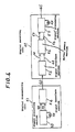
- Fig. 4 is a general block diagram of a digital signal transmitting and receiving apparatus according to the present invention, in which a formatted digital signal is transmitted from a digital transmitting unit 51 to a digital receiving unit 52.
- the digital transmitting unit 51 includes a signal processing section 53, such as a a CD (compact disc) player, which produces an output digital signal on a signal line 58 and a corresponding clock signal on a signal line 59.
- the digital signal consists of successive digital data values, each representing a sample value of an audio signal.
- the clock signal is synchronized with successive bits of this digital signal (assuming serial data transmission to be utilized).
- the digital signal and clock signal of the lines 58 and 59 are inputted to a signal interface section 54, to be converted into a formatted digital signal for transmission to the digital receiving unit 52, using the digital audio interface format described hereinabove with reference to Fig. 3.
- this formatted digital signal is received by a signal interface section 55, which utilizes that signal to produce a recovered clock signal and to convert the formatted digital signal back to the original form of the digital signal which was supplied on line 58 to the signal interface section 54 of the digital transmitting unit 51, i.e. as successive audio sample data values.
- This recovered digital data signal and recovered clock signal are outputted from the signal interface section 55 on signal lines 61 and 62 respectively, to be supplied to a buffer memory section 56.
- the formatted digital signal that is received by the digital receiving unit 52 will include jitter components, and these jitter components will also be present in the recovered digital signal and clock signal that are outputted from the signal interface section 55.
- the recovered digital signal and clock signal will be mutually synchronized, in spite of the jitter components.
- the recovered clock signal can thus be used as in generating successive addresses of the buffer memory 56 into which data of the recovered digital data signal are written.
- the digital receiving unit 52 also includes a signal processing section 57, which receives an output signal from the buffer memory section 56 consisting of successive data values (obtained by read-out of successive addresses of the buffer memory section 56), which corresponds to the digital signal originally outputted from the signal processing section 53 of the digital transmitting unit 51 on signal line 58.
- the signal processing section 57 includes a quartz crystal oscillator whose frequency of operation is determined by a quartz crystal vibrator X R , whereby the signal processing section 57 generates an output clock signal whose frequency is fixed at a value which is nominally identical to that of the clock signal that is supplied on line 59 from the signal processing section 53 of the digital transmitting unit 51. This clock signal produced from the signal processing section 57 is used to generate successive addresses of the buffer memory in the buffer memory section 56, 56 from which data stored therein are read.
- the buffer memory section 56 consists of a buffer memory and an address generating circuit, for generating write and read address values for the buffer memory.
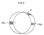
- Fig. 5 is a conceptual diagram to illustrate the memory address relationships
- Fig. 6 is a general block diagram of the address generating circuit.
- the buffer memory is of ring memory configuration. That is to say, as successive read or write address values are generated, when a maximum address value is exceeded, the next address value to be generated is a minimum value.
- the aforementioned write address clock signal is supplied to a write address counter 72 in the address generating circuit of Fig. 6, and successive clock signal pulses counted thereby.
- an initial i.e.
- write address counter 72 which is designated as WR(1) in Fig. 5.
- the write address WR(2) is generated, and so on successively, i.e. incrementing of the write address counter 72 corresponds to clockwise movement around the circle of address values shown in Fig. 5.
- a maximum count value of the write address counter 72 i.e. an address WR(M) is generated, then the next pulse of the write address clock signal will result in the write address WR(1) being generated.
- write address generation is equivalent to successive rotations around the circle of Fig. 5. This is also true of read address generation by a read address counter 74 of the address generating circuit.
- the data contained in the recovered clock signal from the signal interface section 55 are successively written into the buffer memory, with the successive write address being generated based on the recovered clock signal that has been derived from the received digital signal. Since any jitter component of the recovered digital signal will also be present in the recovered clock signal, this jitter will have no effect upon the accuracy of writing data into the buffer memory.
- the read address counter 74 which generates successive memory read addresses is also reset to an initial condition. However the read address counter 74 is reset to an initial count value (designated RE(1) in Fig. 5) which differs from the initial count value (WR(1)) of the write address counter 72 by an amount which is equal to 1/2 of the total number of addresses of the buffer memory. Thus in Fig. 5, the reset address RE(1) is separated from the reset address WR(1) by 180 o .
- each of the write address counter 72 and read address counter 74 is reset to an initial count value of 1, and that there is a total of M addresses in the buffer memory (where M is an integer), then WR(1) will be equal to 1 and RE(1) will be equal to M/2.
- the nominal value of the fixed-frequency clock signal from the signal processing section 57 (used as the read address clock signal in Fig. 6) is identical to that of the recovered clock signal that is used as the write address clock signal, these signals are not mutually frequency-locked. Thus, there will be some degree of frequency difference between the write address clock signal and read address clock signal of the buffer memory. As a result, after simultaneous resetting of the write address counter 72 and read address counter 74 has been executed, and writing and reading of the buffer memory to/from addresses WR(1) and RE(1) respectively begins, then although both the write and read address values can be considered to move in the clockwise direction around the ring of Fig. 5, there will be a fixed rate of relative movement between the read and write address values.
- the write addresses can be considered to move clockwise relative to the read addresses, and similarly the write addresses will move counter-clockwise relative to the read addresses if the frequency of the write address clock signal is lower than that of the read address clock signal.
- any jitter component of the write address clock signal will result in fluctuating small amounts of clockwise and counter-clockwise movement of the write address values relative to the read address values, as viewed in Fig. 5.
- a condition will eventually be reached in which the write and read addresses have approached coincidence, as illustrated by WR(P) and RE(P) in Fig. 5.
- the write address value produced from the write address counter 72 is supplied to one set of inputs of a data selector 78 and to one set of outputs of a subtractor 76, and the count value produced from the read address counter 74 is supplied to one set of inputs of an adder 75.
- a value equal to half of the total number of addresses of the buffer memory (e.g. M/2) is supplied to the other set of inputs of the adder 75.
- the sum value that is thereby obtained from the adder 75, which constitutes the read address value, is supplied to the other set of inputs of the data selector 78 and to the other set of inputs of the subtractor 76.
- a gate signal applied to the data selector 78 controls the selection of the input signals applied thereto, i.e.
- the write address from the write address counter 72 is transferred out of the data selector 78 to be supplied to the buffer memory via signal lines 79, while when the gate signal is at the low logic level, the read address from the adder 75 is transferred out of the data selector 78 and supplied to the buffer memory via the signal lines 79.
- the gate signal is held at the high level during each write cycle of the buffer memory and at the low level during each read cycle.
- the subtractor 76 serves to obtain the difference between the current write and read address values. This difference is compared (in a comparator 77) with a fixed threshold value T V , which is selected to be sufficiently high to ensure that the condition shown as WR(P) and RE(P) in Fig. 5 will never be reached. That is to say, when the difference between the write and read address values falls to this threshold value (as a result of a frequency difference between the write address clock signal and read address clock signal as described above), a reset signal is generated from the comparator 77 which is applied to respective reset input terminals of the write address counter 72 and read address counter 74. Thus when such a reset operation occurs, the write and read address values are respectively set to the initial values WR(1) and WR(2) shown in Fig.
- the present invention enables two mutually independent clock signals to be utilized for write and read operations of the buffer memory, i.e. a recovered clock signal obtained by self-clocking operation is used in write operations, while a fixed-frequency clock signal generated from a quartz crystal oscillator is used for read operations.
- a recovered clock signal obtained by self-clocking operation is used in write operations
- a fixed-frequency clock signal generated from a quartz crystal oscillator is used for read operations.
- a digital signal transmitting and receiving apparatus includes a transmitting unit (51) producing a transmitted digital signal which is formatted to enable self-clocking operation of a receiving unit (52), and a recovered clock signal generated thereby in the receiving unit is used in writing successive received data values into a buffer memory (56). Readout of data from the buffer memory is based on a fixed-frequency clock signal which is independent of the recovered clock signal, so that an output data signal can be obtained which is free from the effects of jitter contained in the input digital signal supplied to the receiving unit.
Landscapes
- Engineering & Computer Science (AREA)
- Computer Hardware Design (AREA)
- Computer Networks & Wireless Communication (AREA)
- Signal Processing (AREA)
- Multimedia (AREA)
- Synchronisation In Digital Transmission Systems (AREA)
- Signal Processing For Digital Recording And Reproducing (AREA)
- Communication Control (AREA)
- Time-Division Multiplex Systems (AREA)
Applications Claiming Priority (2)
| Application Number | Priority Date | Filing Date | Title |
|---|---|---|---|
| JP321039/88 | 1988-12-19 | ||
| JP63321039A JPH02165752A (ja) | 1988-12-19 | 1988-12-19 | ディジタル機器 |
Publications (2)
| Publication Number | Publication Date |
|---|---|
| EP0374794A2 true EP0374794A2 (fr) | 1990-06-27 |
| EP0374794A3 EP0374794A3 (fr) | 1991-10-09 |
Family
ID=18128121
Family Applications (1)
| Application Number | Title | Priority Date | Filing Date |
|---|---|---|---|
| EP19890123387 Withdrawn EP0374794A3 (fr) | 1988-12-19 | 1989-12-18 | Circuit numérique d'émission et de réception utilisant une mémoire tampon pour éliminer des effets de gigue |
Country Status (2)
| Country | Link |
|---|---|
| EP (1) | EP0374794A3 (fr) |
| JP (1) | JPH02165752A (fr) |
Cited By (3)
| Publication number | Priority date | Publication date | Assignee | Title |
|---|---|---|---|---|
| GB2253766A (en) * | 1991-03-15 | 1992-09-16 | Nec Corp | Demultiplexing digital signals and smoothing jitter |
| FR2737368A1 (fr) * | 1996-06-28 | 1997-01-31 | Thomson Multimedia Sa | Procede et dispositif de synchronisation d'horloge d'encodeurs et decodeurs numeriques |
| WO1998056126A1 (fr) * | 1997-06-06 | 1998-12-10 | Deutsche Telekom Ag | Dispositif et procede pour la reception de donnees transmises par une technique de transmission de donnees asynchrone |
Family Cites Families (4)
| Publication number | Priority date | Publication date | Assignee | Title |
|---|---|---|---|---|
| GB1498498A (en) * | 1975-03-05 | 1978-01-18 | Plessey Co Ltd | Frame aligners for time division multiplex(tdm)communication systems |
| US4056851A (en) * | 1976-09-20 | 1977-11-01 | Rca Corporation | Elastic buffer for serial data |
| US4692894A (en) * | 1984-12-18 | 1987-09-08 | Advanced Micro Devices, Inc. | Overflow/Underflow detection for elastic buffer |
| FR2583238B1 (fr) * | 1985-06-11 | 1988-03-18 | Applic Electro Tech Avance | Dispositif de transmission numerique plesiochrone a memoire tampon etendue |
-
1988
- 1988-12-19 JP JP63321039A patent/JPH02165752A/ja active Pending
-
1989
- 1989-12-18 EP EP19890123387 patent/EP0374794A3/fr not_active Withdrawn
Cited By (6)
| Publication number | Priority date | Publication date | Assignee | Title |
|---|---|---|---|---|
| GB2253766A (en) * | 1991-03-15 | 1992-09-16 | Nec Corp | Demultiplexing digital signals and smoothing jitter |
| AU642590B2 (en) * | 1991-03-15 | 1993-10-21 | Nec Corporation | Method and circuit for demultiplexing digital signals capable of absorbing destuffing jitter |
| GB2253766B (en) * | 1991-03-15 | 1994-12-14 | Nec Corp | Method and circuit for demultiplexing digital signals capable of absorbing destuffing jitter |
| FR2737368A1 (fr) * | 1996-06-28 | 1997-01-31 | Thomson Multimedia Sa | Procede et dispositif de synchronisation d'horloge d'encodeurs et decodeurs numeriques |
| WO1998056126A1 (fr) * | 1997-06-06 | 1998-12-10 | Deutsche Telekom Ag | Dispositif et procede pour la reception de donnees transmises par une technique de transmission de donnees asynchrone |
| US8436938B1 (en) | 1997-06-06 | 2013-05-07 | Deutsche Telekom Ag | Device and method for receiving data transmitted by means of an asynchronous data transmission technique |
Also Published As
| Publication number | Publication date |
|---|---|
| EP0374794A3 (fr) | 1991-10-09 |
| JPH02165752A (ja) | 1990-06-26 |
Similar Documents
| Publication | Publication Date | Title |
|---|---|---|
| US4418406A (en) | Signal wave control circuit | |
| US4054921A (en) | Automatic time-base error correction system | |
| US4409627A (en) | Video signal decoding circuit | |
| EP0434837A1 (fr) | Procede et appareil de reproduction | |
| EP0146636B1 (fr) | Circuit de synchronisation | |
| US4314355A (en) | Apparatus and method for receiving digital data at a first rate and outputting the data at a different rate | |
| US4481648A (en) | Method and system for producing a synchronous signal from _cyclic-redundancy-coded digital data blocks | |
| EP0374794A2 (fr) | Circuit numérique d'émission et de réception utilisant une mémoire tampon pour éliminer des effets de gigue | |
| JPS5923647A (ja) | 直列デ−タ信号の変換方法および変換回路 | |
| US4796243A (en) | Time base correcting apparatus | |
| US4561083A (en) | Memory circuit write-in system | |
| US5444658A (en) | Elastic store memory circuit | |
| US4885750A (en) | Method and apparatus for error correction | |
| SE427146B (sv) | Anordning for att endra tidbasen hos en informationssignal | |
| JPS6131549B2 (fr) | ||
| US5422727A (en) | Facsimile apparatus having magnetic tape recording apparatus for data storage | |
| EP0201935A2 (fr) | Méthode et circuit pour supprimer les données "zéros" consécutives | |
| CA1057849A (fr) | Appareil de lecture et d'ecriture des donnees pour support d'enregistrement magnetique | |
| JP2000022649A (ja) | 再サンプリング装置 | |
| JPS5836037A (ja) | Pcm信号伝送方式 | |
| JPS6334542B2 (fr) | ||
| KR0154696B1 (ko) | 디지탈 기록 재생 장치의 동기 패턴 기록 및 검출회로 | |
| JP2697629B2 (ja) | 速度変換装置 | |
| JPH0227647Y2 (fr) | ||
| JP2553072B2 (ja) | 同期回路 |
Legal Events
| Date | Code | Title | Description |
|---|---|---|---|
| PUAI | Public reference made under article 153(3) epc to a published international application that has entered the european phase |
Free format text: ORIGINAL CODE: 0009012 |
|
| 17P | Request for examination filed |
Effective date: 19891218 |
|
| AK | Designated contracting states |
Kind code of ref document: A2 Designated state(s): DE FR GB |
|
| PUAL | Search report despatched |
Free format text: ORIGINAL CODE: 0009013 |
|
| AK | Designated contracting states |
Kind code of ref document: A3 Designated state(s): DE FR GB |
|
| 17Q | First examination report despatched |
Effective date: 19930727 |
|
| STAA | Information on the status of an ep patent application or granted ep patent |
Free format text: STATUS: THE APPLICATION IS DEEMED TO BE WITHDRAWN |
|
| 18D | Application deemed to be withdrawn |
Effective date: 19931207 |