EP0375262A2 - Elektrothermischer Fühler - Google Patents
Elektrothermischer Fühler Download PDFInfo
- Publication number
- EP0375262A2 EP0375262A2 EP89313033A EP89313033A EP0375262A2 EP 0375262 A2 EP0375262 A2 EP 0375262A2 EP 89313033 A EP89313033 A EP 89313033A EP 89313033 A EP89313033 A EP 89313033A EP 0375262 A2 EP0375262 A2 EP 0375262A2
- Authority
- EP
- European Patent Office
- Prior art keywords
- insulating layer
- electrically insulating
- disposed
- thermistor
- heater
- Prior art date
- Legal status (The legal status is an assumption and is not a legal conclusion. Google has not performed a legal analysis and makes no representation as to the accuracy of the status listed.)
- Withdrawn
Links
Images

Classifications
-
- H—ELECTRICITY
- H02—GENERATION; CONVERSION OR DISTRIBUTION OF ELECTRIC POWER
- H02H—EMERGENCY PROTECTIVE CIRCUIT ARRANGEMENTS
- H02H3/00—Emergency protective circuit arrangements for automatic disconnection directly responsive to an undesired change from normal electric working condition with or without subsequent reconnection ; integrated protection
- H02H3/08—Emergency protective circuit arrangements for automatic disconnection directly responsive to an undesired change from normal electric working condition with or without subsequent reconnection ; integrated protection responsive to excess current
- H02H3/085—Emergency protective circuit arrangements for automatic disconnection directly responsive to an undesired change from normal electric working condition with or without subsequent reconnection ; integrated protection responsive to excess current making use of a thermal sensor, e.g. thermistor, heated by the excess current
-
- H—ELECTRICITY
- H02—GENERATION; CONVERSION OR DISTRIBUTION OF ELECTRIC POWER
- H02H—EMERGENCY PROTECTIVE CIRCUIT ARRANGEMENTS
- H02H6/00—Emergency protective circuit arrangements responsive to undesired changes from normal non-electric working conditions using simulators of the apparatus being protected, e.g. using thermal images
Definitions
- This invention relates to an electrothermal sensor which is used as a thermal analog for a wire to be protected against thermal buildup.
- Aerospace solid state power controllers require a low cost, reliable electrothermal sensor to serve as a thermal analog to the wires to be protected by the SSPC.
- Prior art sensors of this type as shown in the commonly assigned copending application, Serial No. 07/224,153, filed July 26, 1988, utilize nickel on polyimide thermistors which are adhesively bonded to a heater/shunt, the wires being delicately soldered to the thermistor contact pads.
- Each sensor of this type has been proposed to be made individually. It is readily apparent that such sensors are relatively expensive to fabricate, particularly in matching thermistor components of the sensors. It is therefore apparent that the art seeks an electrothermal sensor having the attributes of the prior art which can be fabricated more economically.
- this problem of the prior art is minimized and there is provided a method for making an electrothermal sensor and the sensor itself utilizing the wafer of the heater shunt, hybrid-type processing and subsequent separation into individual surface mounted devices that can be flip mounted.
- An alternative to flip mounting is assembly into an insert-molded lead frame.
- a shunt is initially provided in the form of a high electrical resistance layer having good temperature stability of the electrical resistance, a preferred material displaying such properties being Kovar.
- Bumps for electrical connection to the shunt are positioned on opposite sides thereof and secured to the surface of the shunt. These bumps are formed of electrically conductive material, preferably a heavy plate of copper dipped in solder.
- a first electrically insulating layer typically about 0.001 inches thick and preferably of any conventional electrically insulating glass commonly used in thick film technology and having a coefficient of thermal expansion (CTE) substantially the same as that of the shunt is formed over the shunt with the bumps extending therethrough by standard procedure, such as by thick film techniques.
- a first thermistor is then formed on and in the central region of the first electrically insulating layer by standard methods, such as by thick film techniques, thin film techniques, sputtered thin film techniques, metallo-organic techniques or the like.
- This thermistor is a high resistance region formed preferably of any conventional thick film thermistor material embodying metal and other inorganic oxides or the like in a glassy matrix. Other conventional materials, such as nickel, iron or platinum can be used.
- Lines extending from the first thermistor to a second set of bumps for external connection thereto are formed in known manner, such as by the techniques used in thermistor formation, preferably of palladium/silver or the like. Photochemical etching is required for fine thermistor and/or heater lines to provide the desired high resistances.
- the pair of bumps for connection to the ends of the lines connected to the thermistor are secured to the surface of the first electrically insulating layer.
- a third pair of bumps similar to the second pair of bumps and formed along therewith is connected to the ends of conductors on said first electrically insulating layer which connect together two smaller thermistors formed at opposing edge regions of said first electrically insulating layer by the techniques described hereinabove.
- These smaller thermistors are preferably formed of the same material as said first thermistor and,in combination, are equal in resistance to the resistance of the first thermistor.
- a second electrically insulating layer preferably of glass and having a coefficient of thermal expansion (CTE) substantially the same as that of the first electrically insulating layer, is formed in the manner described hereinabove for the first electrically insulating layer and disposed over the first electrically insulating layer as well as the thermistors and the conductors thereon.
- the three sets of bumps extend through the second electrically insulating layer, this second layer being provided to protect the thermistors and conductors as well as to plug up any pinholes or the like existing in the first electrically insulating layer.
- a non-oxidizing nitrogen atmosphere or a protective coating may be provided to avoid metal oxidation during processing of Kovar materials and the like.
- the sensor is then secured to an alumina board or the like with the shunt layer being positioned remote from the board.
- This temperature difference which is measured in terms of change in resistance of the thermistors via parameter measurements obtained at the bumps spanning the respective thermistors and correlates to the amount of energy in the analog wire being monitored for prevention against burn out.
- the difference in resistance relative to the first thermistor exceeds some predetermined value, the measured parameter will indicate this and the system will provide a desired indication, alarm or the like so that the circuit containing the actual, as opposed to the analog wire can be shut down or otherwise operated upon.
- a ceramic substrate preferably aluminum oxide
- a coating of palladium/silver is selectively formed thereon by standard techniques.
- Current is introduced thereto at one end and withdrawn at the opposite end to provide a heating element in the portion of the substrate containing the heater.
- a glass dielectric is then formed over at least the heater and preferably the entire surface of the substrate containing the heater by standard techniques.
- Thick film thermistors and connectors therefor are then formed on the dielectric, one over a closely adjacent the heater and the second at a predetermined distance therefrom. The temperature difference between the two thermistor locations will result different resistances of the thermistors which can be used as an indication of the current in the heater in well known manner. Proper sizing of the substrate and the heater and proper location of the thermistors can allow a unity of current/time/temperature characteristics to be realized.
- Such a device can be used as the sensing element of a solid state power controlling device.
- a conductor in the form of a heater and pads are formed on a ceramic substrate such as steatite.
- a dielectric is then selectively formed in two separate layers over the substrate with apertures therein over the pads and opposite ends of the heater.
- Conductors are then formed over the dielectric and negative temperature coefficient of resistance (NTC) or positive temperature coefficient of resistance (PTC) thermistors are formed in contact with certain ones of the conductors, other ones of the conductors contacting the pads on the substrate or the heater.
- a polymer overcoat is applied over the entire substrate for mechanical protection except for the solder pads to permit contact thereto.
- the ceramic substrate is preferably steatite and the dielectric is preferably glass as noted previously.
- the heater as set forth in the third embodiment can have any one of many desired shapes to be operable. However, in the case of most shapes utilized it has been found that the heater develops hot spots in certain locations, this being undesirable since, it is believed, these hot spots result in unanticipated heat transfer variations and incorrect trip times. Where the heater is in the shape of a horseshoe with a long slot portion, it was found, for example, that an undesired hot spot developed at the end of the slot. Accordingly, designs were investigated wherein the hot spots could be eliminated or at least minimized. In this regard, it was found that the hot spot at the end of the slot in the horseshoe shaped heater was minimized by decreasing the length of the slot.
- a still better result was obtained by retaining the long slot and forming a triangular region at the end of the slot.
- a yet better result was obtained by forming a rectangle at the end of the slot and also forming a cut out region forward of the rectangle on both sides of the slot.
- the new geometries in all cases, appears to minimize the buildup of current around corners either by enlarging the available errors around the corners or by directing current flow away from a small area corner whereby the current path is spread out rather that concentrated at the corners or bends.
- the new geometries as set forth hereinabove provide more generally uniform temperature throughout the heater with the elimination or minimization of hot spots.
- FIGURES 1 and 2 there is shown an electrothermal sensor in accordance with a first embodiment of the invention.
- the sensor includes a Kovar shunt 5 in the form of a high electrical resistance layer having good temperature stability of the electrical resistance.
- Bumps 1 for electrical connection to the shunt 5 are positioned on opposite sides thereof and secured to the surface of the shunt, the bumps being formed of electrically conductive material, preferably a heavy plate of copper dipped in solder.
- a first glass electrically insulating layer 2 of any conventional glass insulating material used in thick film technology having a coefficient of thermal expansion (CTE) substantially the same as that of the shunt 5 and typically of a thickness in the range from 0.0005 to 0.002 inches is formed over the shunt with the bumps 1 extending therethrough by standard procedure, such as by thick film techniques.
- CTE coefficient of thermal expansion
- a first thermistor 3 is then formed on and in the central region of the first electrically insulating layer 2 by standard methods, such as by thick film techniques, thin film techniques, sputtered thin film techniques, metallo organic techniques or the like.
- This thermistor 3 is a high resistance region formed preferably of any thick film thermistor embodying metal and other inorganic oxides or the like in a glassy matrix adapted to display greater than 1000 ppm/°C. resistance change with temperature change.
- Lines 6 and 7 extending from the first thermistor 3 to a second set of bumps 8 for external connection thereto are formed in known manner, such as by the techniques used in thermistor formation, preferably of palladium/silver or the like. Photochemical etching is utilized in the event fine thermistor and/or heaterlines are required to provide a desired high resistance.
- the pair of bumps 8 for connection to the ends of the lines 6 and 7 are secured to the surface of the first electrically insulating layer 2.
- the thermistors 12 and 13 are connected together via a conductor 14 of the same material and formed simultaneously with the conductors 10 and 11, These smaller thermistors 12 and 13 are preferably formed of the same material as the first thermistor and, in combination, are equal in resistance to the resistance of the first thermistor.
- the three sets of bumps 1, 8 and 9 extend through the second electrically insulating layer 4, this second insulating layer being provided to protect the thermistors and conductors on the first insulating layer as well as to plug up any pinholes or the like existing in the first electrically insulating layer.
- a non-oxidizing nitrogen atmosphere or the like or a protective coatings may be provided during fabrication to avoid metal oxidation of Kovar, copper or silver materials and the like during processing.
- the sensor is then secured to an alumina board or the like with the shunt layer being positioned remote from the board.
- This temperature difference is measured in terms of change in resistance of the thermistors via parameter measurements obtained at the bumps 8 and 9 spanning the respective thermistors 3, 12 and 13 and correlates to the amount of energy in the analog wire being monitored for prevention against burn out.
- the difference in resistance of the first thermistor 3 and thermistors 12 and 13 exceeds some predetermined value, the measured parameters will indicate this and the system will provide a desired indication, alarm or the like so that the circuit containing the actual, as opposed to the analog, wire can be shut down or otherwise operated upon.
- a glass dielectric layer 24 is then formed over at least the heater 21 and preferably the entire surface of the substrate 20 containing the heater by standard techniques.
- Thick film thermistors 25 and 26 are then formed on the dielectric 24, Thermistor 26 over or closely adjacent the heater and thermistor 25 at a predetermined remote distance therefrom.
- the thermistor 26 is coupled via lines 27 and 28 to pads 29 whereas thermistor 25 is coupled vial line 30 and 31 to pads 32. The temperature difference between the two thermistor locations will result in different resistances of the thermistors which can be used as an indication of the current in the heater in well known manner.
- a conductor in the form of a heater 40 and thermistor connector pads 41 is formed on a ceramic substrate 42.
- a dielectric 43 is then selectively formed in two separate layers over the substrate with apertures 44 therein disposed over the pads 41 and over opposite ends of the heater 40.
- Conductors 45 are then formed over the dielectric 43 and negative temperature coefficient of resistance (NTC) or positive temperature coefficient of resistance (PTC) thermistors 46 and 47 are formed in contact with certain ones of the conductors 45, other ones of the conductors contacting the pads 41 on the substrate or the heater 40.
- a polymer overcoat (not shown) is applied over the entire substrate except for the solder pads for mechanical protection to permit contact thereto.
- the ceramic substrate is preferably steatite and the dielectric is preferably glass as noted above.
- the embodiment of FIGURE 5 is formed by printing the heater and pads 40 and 41 onto the substrate 40 in standard manner and firing at about 900°C. for about 10 minutes.
- the dielectric 43 is then selectively formed over the substrate and conductors in two separate layers, each layer being separately deposited and fired at about 850°C. for about 10 minutes.
- the conductors 45 are then deposited over the dielectric 43 in standard manner and fired at about 850°C. for about 10 minutes.
- the thermistors 46 and 47 are deposited in standard manner and fired at about 850°C. for about 10 minutes.
- the polymer overcoat is then applied over the entire substrate except the solder pad apertures 44 and is cured at about 165°C. for about 25 minutes.
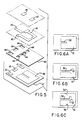
- the heater 40 as set forth in the third embodiment can have any one of many desired shapes to be operable. However, in the case of most shapes utilized, it has been found that the heater develops hot spots in certain locations. This is undesirable since, it is believed, these hot spots result in unanticipated heat transfer variations and the like and incorrect trip times. Where the heater is in the shape of a horseshoe (as shown in FIGURE 5) with two leg portions joined by a back portion and with a long slot portion between the two leg portion, it was found, for example, that a hot spot developed at the end of the slot. Accordingly, designs were investigated wherein the hot spots could be eliminated or at least minimized.
- the hot spot at the end of the slot 50 in the horseshoe shaped heater 51 was minimized by decreasing the length of the slot as shown in FIGURE 6A whereby the distance from the end of the slot 50 to the back edge of the back portion was of greater length than the distance across a leg in a direction normal to the slot.
- a still better result was obtained by retaining the long slot and forming a triangular region 52 at the end of the slot 51.
- a yet better result was obtained by forming a rectangle 53 at the end of the slot 50 and also forming a cut out region 54 and 55 forward of the rectangle on both sides of the slot.
- the new geometries in all cases, appears to minimize the buildup of current around corners either by enlarging the available errors around the corners or by directing current flow away from a small area corner whereby the current path is spread out rather that concentrated at the corners or bends.
- the new geometries as set forth hereinabove provide an essentially constant heat through out the heater with the elimination or minimization of hot spots.
- the heater is formed of titanium metal and the sensors comprise either thermistors as previously described, particularly when provided on an alumina insulating layer on the titanium metal, or commercially available temperature transducers which utilize silicon semiconductor devices.
- the titanium shunt and electrically insulator layer as previously described are bonded together by use of any conventional electrically insulative adhesive or the like and electrical connections are made to the sensors by wire bonds or the like using either ball bonding or ultrasonic bonding.
- Preferably thick film copper pads are screened onto the titanium shunt for electrical attachment of the shunt into a main SSPC circuit or the like. In that arrangement, the thermal conductivity characteristics of titanium metal permit substantial miniaturization of the ETS to facilitate accommodation of the ETS in SSPC device enclosures or the like.
Landscapes
- Thermistors And Varistors (AREA)
- Measuring Temperature Or Quantity Of Heat (AREA)
Applications Claiming Priority (2)
| Application Number | Priority Date | Filing Date | Title |
|---|---|---|---|
| US289294 | 1988-12-22 | ||
| US07/289,294 US5057811A (en) | 1988-12-22 | 1988-12-22 | Electrothermal sensor |
Publications (2)
| Publication Number | Publication Date |
|---|---|
| EP0375262A2 true EP0375262A2 (de) | 1990-06-27 |
| EP0375262A3 EP0375262A3 (de) | 1991-07-17 |
Family
ID=23110899
Family Applications (1)
| Application Number | Title | Priority Date | Filing Date |
|---|---|---|---|
| EP19890313033 Withdrawn EP0375262A3 (de) | 1988-12-22 | 1989-12-13 | Elektrothermischer Fühler |
Country Status (3)
| Country | Link |
|---|---|
| US (1) | US5057811A (de) |
| EP (1) | EP0375262A3 (de) |
| JP (1) | JPH02213733A (de) |
Families Citing this family (19)
| Publication number | Priority date | Publication date | Assignee | Title |
|---|---|---|---|---|
| DE3733192C1 (de) * | 1987-10-01 | 1988-10-06 | Bosch Gmbh Robert | PTC-Temperaturfuehler sowie Verfahren zur Herstellung von PTC-Temperaturfuehlerelementen fuer den PTC-Temperaturfuehler |
| US5161541A (en) * | 1991-03-05 | 1992-11-10 | Edentec | Flow sensor system |
| US5251636A (en) * | 1991-03-05 | 1993-10-12 | Case Western Reserve University | Multiple thin film sensor system |
| US5852397A (en) | 1992-07-09 | 1998-12-22 | Raychem Corporation | Electrical devices |
| US5274350A (en) * | 1992-12-04 | 1993-12-28 | Texas Instruments Incorporated | Shunt apparatus for current sensing and power hybrid circuits |
| DE4328791C2 (de) * | 1993-08-26 | 1997-07-17 | Siemens Matsushita Components | Hybrid-Thermistortemperaturfühler |
| JPH10500255A (ja) | 1994-05-16 | 1998-01-06 | レイケム・コーポレイション | Ptc抵抗素子を含む電気デバイス |
| US5550526A (en) * | 1994-12-27 | 1996-08-27 | Lucent Technologies Inc. | Thermal detection elements with heater |
| US5980785A (en) * | 1997-10-02 | 1999-11-09 | Ormet Corporation | Metal-containing compositions and uses thereof, including preparation of resistor and thermistor elements |
| US6312452B1 (en) | 1998-01-23 | 2001-11-06 | Innercool Therapies, Inc. | Selective organ cooling catheter with guidewire apparatus and temperature-monitoring device |
| DE19851966A1 (de) * | 1998-11-11 | 2000-05-18 | Bosch Gmbh Robert | Keramisches Schichtsystem und Verfahren zur Herstellung einer keramischen Heizeinrichtung |
| US7109842B1 (en) * | 1998-12-07 | 2006-09-19 | Honeywell International Inc. | Robust fluid flow and property microsensor made of optimal material |
| US6794981B2 (en) | 1998-12-07 | 2004-09-21 | Honeywell International Inc. | Integratable-fluid flow and property microsensor assembly |
| US6854176B2 (en) * | 1999-09-14 | 2005-02-15 | Tyco Electronics Corporation | Process for manufacturing a composite polymeric circuit protection device |
| US6640420B1 (en) | 1999-09-14 | 2003-11-04 | Tyco Electronics Corporation | Process for manufacturing a composite polymeric circuit protection device |
| US6365880B1 (en) * | 2000-12-19 | 2002-04-02 | Delphi Technologies, Inc. | Heater patterns for planar gas sensors |
| JP2005040408A (ja) * | 2003-07-24 | 2005-02-17 | Olympus Corp | 発熱素子 |
| WO2006055946A1 (en) * | 2004-11-19 | 2006-05-26 | Conair Corporation | Hair dryers containing high-watt density ceramic heaters |
| GB2522639A (en) * | 2014-01-30 | 2015-08-05 | Nokia Technologies Oy | An apparatus and associated methods for temperature sensing |
Family Cites Families (8)
| Publication number | Priority date | Publication date | Assignee | Title |
|---|---|---|---|---|
| GB838298A (en) * | 1956-06-21 | 1960-06-22 | Reyrolle A & Co Ltd | Improvements in or relating to electric protective relay devices |
| US4023094A (en) * | 1972-06-23 | 1977-05-10 | Adams Robert P | Electronic thermometer |
| US4041440A (en) * | 1976-05-13 | 1977-08-09 | General Motors Corporation | Method of adjusting resistance of a thick-film thermistor |
| US4510482A (en) * | 1982-12-15 | 1985-04-09 | Tektronix, Inc. | Protective circuit for electronic test probes |
| JPS6022302A (ja) * | 1983-07-18 | 1985-02-04 | 松下電器産業株式会社 | サ−ミスタ用酸化物半導体 |
| US4772866A (en) * | 1986-04-11 | 1988-09-20 | Willens Ronald H | Device including a temperature sensor |
| DE3784612T2 (de) * | 1986-09-26 | 1993-09-02 | Sumitomo Electric Industries | Thermistor und verfahren zu seiner herstellung. |
| US4866559A (en) * | 1988-07-26 | 1989-09-12 | Texas Instruments Incorporated | Solid state circuit protector |
-
1988
- 1988-12-22 US US07/289,294 patent/US5057811A/en not_active Expired - Fee Related
-
1989
- 1989-12-13 EP EP19890313033 patent/EP0375262A3/de not_active Withdrawn
- 1989-12-19 JP JP1329428A patent/JPH02213733A/ja active Pending
Also Published As
| Publication number | Publication date |
|---|---|
| JPH02213733A (ja) | 1990-08-24 |
| US5057811A (en) | 1991-10-15 |
| EP0375262A3 (de) | 1991-07-17 |
Similar Documents
| Publication | Publication Date | Title |
|---|---|---|
| US5057811A (en) | Electrothermal sensor | |
| CN100538920C (zh) | 具有钨/氮化铝的稳定高温传感器/加热器系统 | |
| USRE39660E1 (en) | Surface mounted four terminal resistor | |
| EP0517306B1 (de) | Durch Wärme ausgelöste Sicherung mit Schmelzglied | |
| US3978443A (en) | Fusible resistor | |
| US5197804A (en) | Resistance temperature sensor | |
| GB1573235A (en) | Heated sensor for use on aircraft and a method of making such a sensor | |
| GB2148676A (en) | Ceramic heater having temperature sensor integrally formed thereon | |
| CA1040746A (en) | Thin film resistance temperature detector | |
| US6392528B1 (en) | Circuit protection devices | |
| US6082609A (en) | Process for producing a sensor arrangement for measuring temperature | |
| US4160969A (en) | Transducer and method of making | |
| US5652562A (en) | Thermally fused resistor having a portion of a solder loop thermally connected to an electrically insulated portion of an outer surface of the resistor | |
| US5274350A (en) | Shunt apparatus for current sensing and power hybrid circuits | |
| JPS6039510A (ja) | 液面検出素子 | |
| US6121766A (en) | Current sensor assemblies | |
| JP2007093453A (ja) | 表面実装型温度センサ | |
| JP2005510079A (ja) | サージ電流チップ抵抗 | |
| US4419652A (en) | Temperature sensor | |
| US5958606A (en) | Substrate structure with adhesive anchoring-seams for securely attaching and boding to a thin film supported thereon | |
| KR100228146B1 (ko) | 측온저항체 소자의 저항온도계수의 조정방법 및 측온저항체 소자의 제조방법 | |
| JP2996161B2 (ja) | 白金感温抵抗体 | |
| JPH0577737U (ja) | 薄膜測温抵抗体 | |
| JPH0883880A (ja) | 温度センサ付き半導体パッケージ | |
| GB2136206A (en) | Fused ceramic capacitor |
Legal Events
| Date | Code | Title | Description |
|---|---|---|---|
| PUAI | Public reference made under article 153(3) epc to a published international application that has entered the european phase |
Free format text: ORIGINAL CODE: 0009012 |
|
| AK | Designated contracting states |
Kind code of ref document: A2 Designated state(s): DE FR GB IT NL |
|
| PUAL | Search report despatched |
Free format text: ORIGINAL CODE: 0009013 |
|
| AK | Designated contracting states |
Kind code of ref document: A3 Designated state(s): DE FR GB IT NL |
|
| 17P | Request for examination filed |
Effective date: 19911119 |
|
| 17Q | First examination report despatched |
Effective date: 19930316 |
|
| STAA | Information on the status of an ep patent application or granted ep patent |
Free format text: STATUS: THE APPLICATION HAS BEEN WITHDRAWN |
|
| 18W | Application withdrawn |
Withdrawal date: 19930602 |
|
| R18W | Application withdrawn (corrected) |
Effective date: 19930602 |