EP0375342A2 - Appareil pour l'enregistrement/la reproduction de données sur un disque pour l'enregistrement - Google Patents
Appareil pour l'enregistrement/la reproduction de données sur un disque pour l'enregistrement Download PDFInfo
- Publication number
- EP0375342A2 EP0375342A2 EP19890313251 EP89313251A EP0375342A2 EP 0375342 A2 EP0375342 A2 EP 0375342A2 EP 19890313251 EP19890313251 EP 19890313251 EP 89313251 A EP89313251 A EP 89313251A EP 0375342 A2 EP0375342 A2 EP 0375342A2
- Authority
- EP
- European Patent Office
- Prior art keywords
- equalizer
- signal
- output
- analog
- digital converter
- Prior art date
- Legal status (The legal status is an assumption and is not a legal conclusion. Google has not performed a legal analysis and makes no representation as to the accuracy of the status listed.)
- Granted
Links
Images


Classifications
-
- G—PHYSICS
- G11—INFORMATION STORAGE
- G11B—INFORMATION STORAGE BASED ON RELATIVE MOVEMENT BETWEEN RECORD CARRIER AND TRANSDUCER
- G11B7/00—Recording or reproducing by optical means, e.g. recording using a thermal beam of optical radiation by modifying optical properties or the physical structure, reproducing using an optical beam at lower power by sensing optical properties; Record carriers therefor
-
- G—PHYSICS
- G11—INFORMATION STORAGE
- G11B—INFORMATION STORAGE BASED ON RELATIVE MOVEMENT BETWEEN RECORD CARRIER AND TRANSDUCER
- G11B20/00—Signal processing not specific to the method of recording or reproducing; Circuits therefor
- G11B20/10—Digital recording or reproducing
- G11B20/10009—Improvement or modification of read or write signals
- G11B20/10037—A/D conversion, D/A conversion, sampling, slicing and digital quantisation or adjusting parameters thereof
-
- G—PHYSICS
- G11—INFORMATION STORAGE
- G11B—INFORMATION STORAGE BASED ON RELATIVE MOVEMENT BETWEEN RECORD CARRIER AND TRANSDUCER
- G11B11/00—Recording on or reproducing from the same record carrier wherein for these two operations the methods are covered by different main groups of groups G11B3/00 - G11B7/00 or by different subgroups of group G11B9/00; Record carriers therefor
- G11B11/10—Recording on or reproducing from the same record carrier wherein for these two operations the methods are covered by different main groups of groups G11B3/00 - G11B7/00 or by different subgroups of group G11B9/00; Record carriers therefor using recording by magnetic means or other means for magnetisation or demagnetisation of a record carrier, e.g. light induced spin magnetisation; Demagnetisation by thermal or stress means in the presence or not of an orienting magnetic field
- G11B11/105—Recording on or reproducing from the same record carrier wherein for these two operations the methods are covered by different main groups of groups G11B3/00 - G11B7/00 or by different subgroups of group G11B9/00; Record carriers therefor using recording by magnetic means or other means for magnetisation or demagnetisation of a record carrier, e.g. light induced spin magnetisation; Demagnetisation by thermal or stress means in the presence or not of an orienting magnetic field using a beam of light or a magnetic field for recording by change of magnetisation and a beam of light for reproducing, i.e. magneto-optical, e.g. light-induced thermomagnetic recording, spin magnetisation recording, Kerr or Faraday effect reproducing
- G11B11/10502—Recording on or reproducing from the same record carrier wherein for these two operations the methods are covered by different main groups of groups G11B3/00 - G11B7/00 or by different subgroups of group G11B9/00; Record carriers therefor using recording by magnetic means or other means for magnetisation or demagnetisation of a record carrier, e.g. light induced spin magnetisation; Demagnetisation by thermal or stress means in the presence or not of an orienting magnetic field using a beam of light or a magnetic field for recording by change of magnetisation and a beam of light for reproducing, i.e. magneto-optical, e.g. light-induced thermomagnetic recording, spin magnetisation recording, Kerr or Faraday effect reproducing characterised by the transducing operation to be executed
- G11B11/10515—Reproducing
-
- G—PHYSICS
- G11—INFORMATION STORAGE
- G11B—INFORMATION STORAGE BASED ON RELATIVE MOVEMENT BETWEEN RECORD CARRIER AND TRANSDUCER
- G11B11/00—Recording on or reproducing from the same record carrier wherein for these two operations the methods are covered by different main groups of groups G11B3/00 - G11B7/00 or by different subgroups of group G11B9/00; Record carriers therefor
- G11B11/10—Recording on or reproducing from the same record carrier wherein for these two operations the methods are covered by different main groups of groups G11B3/00 - G11B7/00 or by different subgroups of group G11B9/00; Record carriers therefor using recording by magnetic means or other means for magnetisation or demagnetisation of a record carrier, e.g. light induced spin magnetisation; Demagnetisation by thermal or stress means in the presence or not of an orienting magnetic field
- G11B11/105—Recording on or reproducing from the same record carrier wherein for these two operations the methods are covered by different main groups of groups G11B3/00 - G11B7/00 or by different subgroups of group G11B9/00; Record carriers therefor using recording by magnetic means or other means for magnetisation or demagnetisation of a record carrier, e.g. light induced spin magnetisation; Demagnetisation by thermal or stress means in the presence or not of an orienting magnetic field using a beam of light or a magnetic field for recording by change of magnetisation and a beam of light for reproducing, i.e. magneto-optical, e.g. light-induced thermomagnetic recording, spin magnetisation recording, Kerr or Faraday effect reproducing
- G11B11/10502—Recording on or reproducing from the same record carrier wherein for these two operations the methods are covered by different main groups of groups G11B3/00 - G11B7/00 or by different subgroups of group G11B9/00; Record carriers therefor using recording by magnetic means or other means for magnetisation or demagnetisation of a record carrier, e.g. light induced spin magnetisation; Demagnetisation by thermal or stress means in the presence or not of an orienting magnetic field using a beam of light or a magnetic field for recording by change of magnetisation and a beam of light for reproducing, i.e. magneto-optical, e.g. light-induced thermomagnetic recording, spin magnetisation recording, Kerr or Faraday effect reproducing characterised by the transducing operation to be executed
- G11B11/1053—Recording on or reproducing from the same record carrier wherein for these two operations the methods are covered by different main groups of groups G11B3/00 - G11B7/00 or by different subgroups of group G11B9/00; Record carriers therefor using recording by magnetic means or other means for magnetisation or demagnetisation of a record carrier, e.g. light induced spin magnetisation; Demagnetisation by thermal or stress means in the presence or not of an orienting magnetic field using a beam of light or a magnetic field for recording by change of magnetisation and a beam of light for reproducing, i.e. magneto-optical, e.g. light-induced thermomagnetic recording, spin magnetisation recording, Kerr or Faraday effect reproducing characterised by the transducing operation to be executed to compensate for the magnetic domain drift or time shift
-
- G—PHYSICS
- G11—INFORMATION STORAGE
- G11B—INFORMATION STORAGE BASED ON RELATIVE MOVEMENT BETWEEN RECORD CARRIER AND TRANSDUCER
- G11B11/00—Recording on or reproducing from the same record carrier wherein for these two operations the methods are covered by different main groups of groups G11B3/00 - G11B7/00 or by different subgroups of group G11B9/00; Record carriers therefor
- G11B11/10—Recording on or reproducing from the same record carrier wherein for these two operations the methods are covered by different main groups of groups G11B3/00 - G11B7/00 or by different subgroups of group G11B9/00; Record carriers therefor using recording by magnetic means or other means for magnetisation or demagnetisation of a record carrier, e.g. light induced spin magnetisation; Demagnetisation by thermal or stress means in the presence or not of an orienting magnetic field
- G11B11/105—Recording on or reproducing from the same record carrier wherein for these two operations the methods are covered by different main groups of groups G11B3/00 - G11B7/00 or by different subgroups of group G11B9/00; Record carriers therefor using recording by magnetic means or other means for magnetisation or demagnetisation of a record carrier, e.g. light induced spin magnetisation; Demagnetisation by thermal or stress means in the presence or not of an orienting magnetic field using a beam of light or a magnetic field for recording by change of magnetisation and a beam of light for reproducing, i.e. magneto-optical, e.g. light-induced thermomagnetic recording, spin magnetisation recording, Kerr or Faraday effect reproducing
- G11B11/1055—Disposition or mounting of transducers relative to record carriers
- G11B11/10576—Disposition or mounting of transducers relative to record carriers with provision for moving the transducers for maintaining alignment or spacing relative to the carrier
-
- G—PHYSICS
- G11—INFORMATION STORAGE
- G11B—INFORMATION STORAGE BASED ON RELATIVE MOVEMENT BETWEEN RECORD CARRIER AND TRANSDUCER
- G11B20/00—Signal processing not specific to the method of recording or reproducing; Circuits therefor
- G11B20/10—Digital recording or reproducing
-
- G—PHYSICS
- G11—INFORMATION STORAGE
- G11B—INFORMATION STORAGE BASED ON RELATIVE MOVEMENT BETWEEN RECORD CARRIER AND TRANSDUCER
- G11B20/00—Signal processing not specific to the method of recording or reproducing; Circuits therefor
- G11B20/10—Digital recording or reproducing
- G11B20/10009—Improvement or modification of read or write signals
- G11B20/10046—Improvement or modification of read or write signals filtering or equalising, e.g. setting the tap weights of an FIR filter
-
- G—PHYSICS
- G11—INFORMATION STORAGE
- G11B—INFORMATION STORAGE BASED ON RELATIVE MOVEMENT BETWEEN RECORD CARRIER AND TRANSDUCER
- G11B20/00—Signal processing not specific to the method of recording or reproducing; Circuits therefor
- G11B20/10—Digital recording or reproducing
- G11B20/10009—Improvement or modification of read or write signals
- G11B20/10222—Improvement or modification of read or write signals clock-related aspects, e.g. phase or frequency adjustment or bit synchronisation
-
- G—PHYSICS
- G11—INFORMATION STORAGE
- G11B—INFORMATION STORAGE BASED ON RELATIVE MOVEMENT BETWEEN RECORD CARRIER AND TRANSDUCER
- G11B20/00—Signal processing not specific to the method of recording or reproducing; Circuits therefor
- G11B20/22—Signal processing not specific to the method of recording or reproducing; Circuits therefor for reducing distortions
-
- G—PHYSICS
- G11—INFORMATION STORAGE
- G11B—INFORMATION STORAGE BASED ON RELATIVE MOVEMENT BETWEEN RECORD CARRIER AND TRANSDUCER
- G11B7/00—Recording or reproducing by optical means, e.g. recording using a thermal beam of optical radiation by modifying optical properties or the physical structure, reproducing using an optical beam at lower power by sensing optical properties; Record carriers therefor
- G11B7/002—Recording, reproducing or erasing systems characterised by the shape or form of the carrier
- G11B7/0037—Recording, reproducing or erasing systems characterised by the shape or form of the carrier with discs
Definitions
- the data format used for recording and reproducing data in an optical disk apparatus is mainly classified into two types of continuous composite servo format and Discrete Block servo Format (hereinafter to be abbreviated as DBF) from the detection method of the tracking signal of light spot and the groove shape on the disk medium.
- DBF Discrete Block servo Format
- the present invention relates to an equalizer of the optical disk apparatus using DBF and an optical disk recording/reproducing apparatus.
- DBF has its characteristics in easiness of detection of tracking signal and stability of clock detection of the recorded and reproduced data, and is designed to detect all the timings using the clock pits written on the disk.
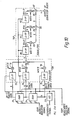
- Fig. 1 shows the signal reproducing section of the conventional magnetooptical disk
- Fig. 2 and Fig. 3 are the waveform diagrams for illustrating the operation thereof
- Fig. 4 is a circuit diagram for the equalization cricuit of the signal reproducing section of the conventional magnetooptical disk.
- the part 1 shows an optical head.
- the optical head is composed of a laser, a lens, an actuator, a polarized beam splitter, a pin photodiode, a prepit signal reproducing circuit, a magnetooptical signal reproducing circuit, etc.
- the part 70 is an optcal disk, 71 is a track, 2 and 3 are the peak hold circuits, 4 is a subtractor, 5 is a differentiator, 7 is a counter, 8 is a switch, 9 is an equalization circuit, 10 is an address decoder, 11 is a system controller.
- 72 is a clock reproducer.
- the clock reproducer 72 is composed of a differentiator 5, a phase locked loop circuit 6, and a counter 7.
- 88 is a servo signal extractor.
- the servo signal extractor 88 is composed of a peak hold circuits 2, 3 and a subtractor 4.
- the part 12 is an analog to digital converter.
- 13 ⁇ 15 are D flip-flops (hereinafter to be abbreviated as D-FFS), 16 ⁇ 18 are multipliers, and 19 and 20 are adders.
- the optical head 1 outputs a focus error signal by an optical spot formed on the magnetooptical disk 70 and outputs the addresses, wobble marks and clock-pits which are unevenly recorded as shown in Fig. 2 as the pre-recording signals of the change in the reflected light amount.
- the data format for recording and reproducing the 3.5 inch magnetooptical disk with enlargement of the track 71 of the disk 70 in Fig. 1 is shown in Fig. 2.
- the data format for recording and reproducing in the 3.5 inch magnetooptical disk is formed by dividing 1 track of a one circulation into 22 sectors, with 1 sector comprising 76 blocks. Of 76 blocks, the 0th block ⁇ second block are the header blocks, being the addresses showing the sector mark, sector number, and track number.
- the third block ⁇ 75th block are the data blocks, in which 1 block is composed of the two servo- bytes and eight data bytes.
- servo-bytes are composed of the wobble marks for tracking error detection and the clock-pits for clock reproduction, as shown in Fig. 2 (c).
- the differentiator 5 differentiates the clock-pit signal which is an input signal and outputs it.
- the phase locked loop circuit 6 has the free running frequency of 110 times the repeating frequency of the clock-pit signal; it accepts the output of said differentiator 5 only in the vicinity of the reproduction timing of the clock-pit by the indication signal of the counter 7; performs phase comparison of the reproduced clock output with the signal made by dividing the reproduced clock output into 110 sections with a counter 7 and synchronizes it.
- the counter 7 is a 110 divisional counter as aforementioned, which divides the aforementioned reproduced clock into 110 sections and at the same time outputs the timing indication signal of the said clock pit and the timing indication signal of the wobble marks.
- the clock reproducer 72 reproduces the clock.
- the servo signal extractor 88 outputs the tracking error signal by the above operation.
- the address signal and the magnetooptical signal are recorded and reproduced in 4-11 modulation.
- the data in the length of 11 bits is allocated to one symbol of the length of 1 byte before modulation, and as its rule modulation is made so that the number of the code "1" after the modulation becomes four in the one symbol of 11 bits.
- the data of 88 bits are recorded and reproduced.
- This state corresponds to 110 bits in the length of one block.
- the write-in clock to be used for recording the magnetooptical signal is a reproduced clock reproduced from the aforementioned clock-pit, and similarly, for equalization and identification of data, the aforementioned reproduced clock is used.
- the address signal and the data signal outputted from the optical head 1 are connected to the switch 8.
- the switch 8 changes over the address signal and the data signal using the switching signal of the system controller 11.
- a circuit diagram of the equalization circuit 9 is shown in Fig. 4.
- the output of the switch 8 is inputted to the analog to digital (AD) converter 12.
- the AD converter 12 converts the analogue address signal and optical magnetic signal into digital signals.
- the sampling signal is a reproduced clock of the phase locked loop circuit 7.
- the clocks of D-FFS 13 - 15 are also similarly the aforementioned reproduced clocks, which output the outputs of AD converter 12 by sequentially delaying by one cycle of the above reproduced clock to the multipliers 16 - 18.
- the multipliers 16 - 18 multiply the aforementioned delayed signals by the coefficients of W(-1) - W(1) and output them to the adders 19 and 20.
- the equalization circuit 9 has an effect of suppressing the wave interference by the adjacent bits of the reproduced signals S6 - S8 as shown in Fig. 3 (a) .
- the address decoder 10 detects the address signal out of the equalization circuit 9 and demodulates the current address.
- the system controller 11 operates by taking in the output of the address demodulator 10 to output the changeover signal for changing over between the address signal and the data signal to the switch 8.
- the optical disk there is given a large memory capacity. This is because, due to the fact that the linear density is equivalent to that of the magnetic disk apparatus at more than 20 Kbpi and the inter-track pitch of the recording track is small at about 1.6 microns, large area density can be obtained. At present, with this characteristic developed further, a further demand for high density has arisen. As a method for realizing this requirement, it is general to expect an increase in the linear density and to reduce the wave interference by using the equalization circuit in the conventional data reproducing section. As another direction, it is considered to make the track pitch smaller to increase the area density. When the track pitch becomes not more than 1 micron, the cross talk from the adjacent track increases. However, in the equalization circuit in the signal reproduction section of the conventional magnetooptical disk, there has been given no consideration at all to the interference from the adjacent track, and there has been a defect of limitation to attaining high density.
- An object of the present invention is to provide the two-dimensional fixed and blind equalizers designed to suppress the wave interference from the adjacent tracks which have never been considered in the conventional one-dimensional equalization circuit and a data recording/reproducing apparatus using a recording disk using such two-dimensional equalizer.
- a data recording/reproducing apparatus using a disk recording medium has an equalizer block comprising: an analog to digital converter for sampling, quantitizing and outputting reproduced signals from the disk recording medium; a memory for storing signal trains of a plurality of tracks outputted from said analog to digital converter; and a wave equalizer for reading out simultaneously the signal trains of a plurality of tracks stored in said memory and performing equalization with respect to both of a wave interference in the longitudinal direction of each track and a wave intereference from an adjacent track.
- the equalizer By the above construction, it is possible to suppress the wave interference from the adjacent track and minimize the reproduced data error rate by cross-talk even in case that the track pitch is narrow. Further, by making the equalizer into a blind equalizer, wave interference fluctuations attributed to linear recording density, irregularity of recording power, optical spot, tracking error, etc. are automatically corrected and suppressed. Furthermore, the blind equalizer may be so constructed as to correct automatically in good efficiency the error and fluctuation of the clock timing.
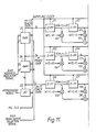
- the part 1 is an optical head.
- 70 is a magnetooptical disk
- 71 is a track
- 2 and 3 are the peak hold circuits
- 4 is a subtractor
- 5 is a differentiator
- 6 is a phase locked loop circuit
- 7 is a counter
- 8 is a switch
- 21 is an equalizer block
- 10 is an address decoder
- 22 is a system controller
- 72 is a clock reproducer
- the clock reproducer 72 is composed of a differentiator 5, a phase locked loop circuit 6 and a counter 7.
- the part 88 is a servo signal extractor, and the servo signal extractor 88 is composed of a peak hold circuits 2, 3 and a subtractor 4.
- the clock reproducer 72 generates a reproduced clock from clock pits in the same manner as in the conventional embodiment.
- the servo signal extractor 88 also outputs a tracking error signal from the maximum values V1 and V2 of the wobble mark signals as shown in Fig. 2 (d).
- the address signal and the data signal outputted from the optical head 1 are connected to the switch 8.
- the switch 8 changes over the address signal and the data signal according to the changeover signal from the system controller 22.
- the equalizer block 21 performs the equalization using the output of the phase locked loop circuit 6, the read/write selection signal for RAM and the address indication signal for RAM of the system controller 22.
- the address decoder 10 detects the address signal out of the outputs of the equalizer block 21 and decodes the current address.
- the system controller 22 is operated by taking in the output of the address decoder 10 to output the selection signal for changing over between the address signal and the data signal to the switch 8, and output the read/write selection signal for RAM and the address indication signal for RAM to the equalizer block 21.
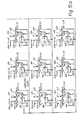
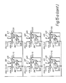
- the equalizer 21 of Fig. 8 the circuit diagram of the first embodiment of the fixed equalizer block is shown in Fig. 9.
- the part 23 is an analog to digital converter
- 24 and 25 are RAMs
- 26 - 30, 40 - 44, 55 - 59 are D - FFS
- 31 - 35, 45 - 49, 60 - 64 are multipliers
- 36 - 39, 50 - 54, 65 - 69 are adders.
- 89 is an equalizer.
- the equalizer 89 is composed of D-FFS 26 - 30, multipliers 31 - 35 and adders 36 - 39.
- 90 is an equalizer.
- the equalizer 90 is composd of D-FF 40 - 44, multipliers 45 - 49 and adders 50 - 53.
- 138 is similarly an equalizer, and is composed of D-FF 55 - 59, multipliers 60 - 64 and adders 65 - 68.
- the analog to digital converter 23 effects analog to digital conversion of the address signal and the data signal of the analog signals which are the outputs of the switch 8 into the digital signals.
- the analog to digital converter 23 employs an output of the phase locked loop circuit 6 as a sampling clock.
- the frequency of the reproduced clock signal is the same as the channel bit rate of the recorded and reproduced data.
- the output of the analog to digital converter 23 is 8 bits.
- the output of the analog to digital converter 23 is memorized in RAMs 24 and 25.
- the capacity of each of the RAMs 24 and 25 is the capacity capable of recording the data of 1 track.
- RAMs 24 and 25 use the output of the phase locked loop circuit as clock and change over between the reading and the writing of the data by the read/write selection signal for RAM which is the output of the system controller 22. Also, the addresses of the RAMs 24 and 25 are changed over by the address indication signal for RAM of the system controller 22.
- the RAM 24 outputs the data of the mth track
- the RAM 25 outputs the data with delay of 1 track from the output of the RAM 24, so that it outputs the data of the (m - 1)th track. Also, at that time the AD converter 23 outputs the data of the (m + 1)th track.
- the equalizers 89, 90 and 138 are the 5-tap transversal filters, and the equalizer 89 performs equalization of the data of the (m - 1)th track.
- the equalizer 90 performs equalization of the mth track, and similarly, the equalizer 138 performs equalization of the (m + 1)th track.
- the adder 54 adds the outputs of the equalizer 89 and the equalizer 90, and the adder 69 adds the outputs of the aforementioned adder 54 and the equalizer 138.
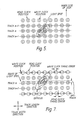
- Fig. 6 is an illustrative view of the 2 dimension arrangement of the sampling of the reproduced signal.
- the white circles represent the clockpits and the black circles signify the positions of the read-out clocks.
- Fig. 5 is an illustrative view of the optical spot shape, in which the central ellipse shows the intensity distribution of the optical spots, and, of the circles on the track, the larger circles show the read clock positions and the smaller circles show the write clock positions.
- the tap coefficient W(k, l) of the equalizer block is determined according to the optical spot shape, recorded pit shape, etc.
- the optical spot in which the intensity distribution can be approximated by Gaussian distribution is dominant to its characteristic, so that the coefficient matrix W(k,l) becomes:
- k -1,0,1
- l -2,-1, etc.
- shows the absolute value.
- the 2-dimensional equalizer block By the abovementioned construction of the 2-dimensional equalizer block, there can be realized a fixed equalizer block and an optical disk recording/reproducing apparatus using such a fixed equalizer block in which both the wave interference from the adjacent tracks and the wave interference of the adjacent bits are suppressed to perform the optimum equalization, and even in case of narrowing of the track pitch, the error rate of the reproduced data by crosstalk can be reduced.
- Fig. 10 shows a circuit diagram of the second embodiment of the fixed equalizer block as the equalizer block 21.
- the numerals 73 - 75 and 80 - 82 are D-FFs, 76 - 78 and 83 - 85 are multipliers, and 79, 86, and 87 are adders.
- 139 is an equalizer.
- the equalizer 139 is composed of D-FFs 73 - 75, multipliers 76 - 78 and adder 79.
- 140 is an equalizer.
- the equalizer 140 is composed of D-FFs 80 - 82, multipliers 83 - 85 and adders 86 and 87.
- the equalizers 139 and 140 are each composed of a 3 tap transversal filter.
- the coefficient matrix w(K, l) beccmes: W(k, l) W1(k) ⁇ W2(l) (2), so that the 2-dimensional coefficient W(k, l) is separable into the coefficient in the longitudinal direction in W1(k) and the coefficient in the latitudinal direction W2(l) Accordingly, the equalizer is separable into the longitudinal direction and the latitudinal direction of the track, and the output y(m, n) of the equalizer block 21 becomes:
- the equalizer 139 is operated to eliminate the cross talk from The adjacent track, and the equalizer 140 to eliminate the wave interference from the adjacent bits in the longitudinal direction of the track.
- the abovementioned embodiment is to give the coefficient to the multiplier in a fixed state. However, by adaptively varying it, the equalization characteristic having the higher effect can be given.
- Fig. 5 shows an illustrative view on the light spot shape.
- the axis of the elliptical light spot intensity distribution as shown in Fig. 5 frequently varies according to the position on the disk for recording and reproducing, i.e., address, and in other system as well, the linear recording density varies according to the address. Therefore, there arises a necessity for the coefficient of the equalizer to be frequently varied.
- the causes for variation of the 2-dimensional recording and reproducing characteristics may be summarized as shown in Fig. 7.
- the factors for determining the equalization characteristic are mainly classified into the light spot shape related to the condition in recording, recording power, recording clock timing, focus, shape of recording pit and position thereof formed by fluctuation of tracking, light spot shape related to the condition in reproducing, tracking, focus, and adjacent symbols and intersymbol interference in the track direction by variation of sampling clock timing. Accordingly, by giving adequate desired signal, adapting of the coefficient to suppress the interference by adaptively following these variations becomes possible.
- LMS method Least Mean Square error method
- the equalized output is sign detected, and, based on the result thereof, determination may be made in consideration of the non-distortion condition of intersymbol interference according to the modulation system in use.
- Fig. 11 is a circuit diagram of an equalizer of the first embodiment of the blind equalizer block
- Fig. 13 is a circuit diagram of the coefficient control circuit of the first embodiment of the blind equalizer block.
- 91 - 95, 105 - 109 and 120 - 124 are D-FFs
- 96 - 100, 110 - 114 and 125 - 129 are multipliers
- 101 - 104, 115 - 119 and 130 - 134 are adders
- 136 is a comparator
- 135 - 137 are subtractors.
- 270 is a sign detector.
- the sign detector 270 is composed of a subtractor 135 and a comparator 136.
- 195 - 239 are multipliers
- 240 - 254 are D-FFs
- 255 - 269 are adders.
- the basic equalizer unit composed of D-FFs 91 - 95, 105 - 109 and 120 - 124, multipliers 96 - 100, 110 - 114 and 125 - 129, and adders 101 - 104, 115 - 119 and 130 - 134 is identical with that shown in Fig. 9.
- the error signal e(m, n) may be operated using the sign detector output a(m, n).
- the substractor 137 outputs the difference between the equalizer output y(m, n) and the desired signal a(m, n) as an error signal e(m, n).
- the coefficient control circuit of Fig. 13 is a circuit to change over the 3 X 5 coefficient matrix W(k, 1) of the equalization circuit of Fig. 11.
- the coefficient control circuit of Fig. 13 is to realize the adaptive algorism of the LMS method, in which, in order to minimize the minimum error average of the error signal e(m, n) of the equalizer of Fig. 11, the coefficient matrix is renewed according to the following equation.
- Literature M. M. Hadhoud, D. W. Thomas, "The Two-Dimensional Adaptive LMS (TDLMS) Algorithm", IEEE Trnsactions on Circuits and Systems, vol.35, No. 5, May 1988, pp. 485 - 494
- the wave interference from the adjacent track can be suppressed, and, in case of narrowing the track pitch, reproduced data error rate by cross talk can be reduced.
- a blind equalizer block and an optical disk recording/reproducing apparatus using such a blind equalizer block in which the interference fluctuation attributed to linear recording density, recording power irregularity, light spot, tracking error, etc. is automatically compensated to suppress such fluctuation.
- Fig. 12 is a circuit diagram of an equalizer of the second embodiment of the blind equalizer block
- Fig. 13 is a circuit diagram of the coefficient control circuit of the second embodiment of the blind equalizer block.
- 141 - 145, 155 - 159, 170 - 174 and 187 - 189 are D-FFs
- 190 and 191 are multipliers
- 151 - 154, 165 - 169, 180 - 184, 192 and 193 are adders
- 186 is a comparator
- 185 and 194 are subtractors.
- 271 is a sign detector.
- the sign detector 271 is composed of a subtractor 185 and a comparator 186, and its output is represented by a(m, n).
- the part 272 is a finite impulse response (FIR) low-pass filter.
- FIR finite impulse response
- the FIR low-pass filter 272 is composed of D-FFs 187 - 189, multipliers 190 and 191, and adders 192 and 193, and performs band limitation of the output signal a(m, n) of the sign detector 271.
- the coefficient of the multipliers 190 and 191 is ⁇ ( ⁇ > 0).
- the wave interference from the adjacent track can be suppressed, and, in case of narrowing the track pitch, reproduced data error rate by cross-talk can be reduced. Also, the interference fluctuation attributed to linear recording density, recording power irregularity, light spot, tracking error, etc. is automatically compensated to suppress such fluctuation. Also, there can be realized a blind equalizer block which improves the signal to noise ratio in comparison with the first embodiment of the blind equalizer block and an optical disk recording/reproducing apparatus using such blind equalizerblock.
- the reproduced clock timing error in recording and reproducing requires to be strictly controlled, because of a large problem of fluctuation of the circuit in the optical head 1 (eg., when, as in the magneto-optical disk apparatus, the reproduction circuit of the clock pit and the reproduction circuit of the magneto-optical data unit are different, the delay time of each circuit becomes irregular or temperature change may be produced).
- the equalizer is a T-spaced linear equalizer, so that the effect of this delay compensation is small. Accordingly, by constituting a T-2 spaced linear equalizer for the reproduced clock as the third embodiment of the blind equalizer block, this delay compensation effect can be rapidly increased.
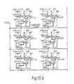
- Fig. 14 shows a circuit diagram of an equalizer of the blind equalizer block of the third embodiment
- Fig. 15 (a). and (b) show the circuit diagrams of the coefficient control circuit of the blind equalizer block of the third embodiment.
- Fig. 14 274 - 282, 300 - 308, 327 - 335 and 356 - 360 are D-FFs, 283 - 291, 309 - 317, 336 - 344 and 361 - 364 are multipliers, 292 - 299, 318 - 326, 345 - 353and 365 - 368 are adders.
- the equalization unit has a construction of 3 X 9 taps so as to doubly increase the clock frequency.
- 355 is comparator
- 354 and 369 are subtractors.
- 273 is a clock generator.
- 507 is a sign detector.
- the sign detector 507 is composed of a subtractor 354 and a comparator 355, and its output is represented by a(m, n) .
- the FIR low-pass filter 508 is a FIR low-pass filter.
- the FIR low-pass filter 508 is composed of D-FFs 356 - 360, multipliers 361 - 364 and adders 365 - 368, and performs band limitation of the output signal a(m, n) of the sign detector 507.
- the coefficient of the multipliers 361 and 364 is ⁇ ( ⁇ > 0), and the coefficient of the multipliers 362 and 363 is ⁇ ( ⁇ > 0) .
- the FIR low-pass filter 508 also has 5-tap construction so as to doubly increase the clock frequency.
- Fig. 15 (a) the parts 370 - 416 are multipliers, 417 - 431 are adders, 432 - 446 are D-FFs.
- the parts 447 - 482 are multiplirs, 483 - 494 are adders, and 495 - 506 are D-FFs.
- the coefficient control circuits of Fig. 15 (a) and (b) are the circuits for changing over the coefficient matrix W(k, l) of the 3 X 9 taps of the equalization circuit of Fig. 14.
- the clock generator 273 causes to generate the clocks of twofold frequency from the reproducing clock of the phase locked loop circuit 7.
- the AD converter 23, RAMs 24, 25, D-FF in Fig. 14, and D-FFs in Figs. 15 and 16 use the signal of the clock generator as a sampling clock.
- the number of taps of the qualizer is 9 taps, and the output y(m, n) of the equalizer is:
- the wave interference from the adjacent track can be suppressed, and, in case of narrowing the track pitch, reproduced data error rate by cross-talk can be reduced. Also, the interference fluctuation attributed to linear recording density, recording power irregularity, light spot, tracking error, etc. is automatically compensated to suppress such fluctuation. Also., there can be realized a blind equalizer block which can automatically efficiently compensate the error of the clock timing and its fluctuation and an optical disk recording/reproducing apparatus using such blind equalizer block.
Landscapes
- Engineering & Computer Science (AREA)
- Signal Processing (AREA)
- Signal Processing For Digital Recording And Reproducing (AREA)
- Optical Recording Or Reproduction (AREA)
Applications Claiming Priority (2)
| Application Number | Priority Date | Filing Date | Title |
|---|---|---|---|
| JP322616/88 | 1988-12-21 | ||
| JP32261688 | 1988-12-21 |
Publications (3)
| Publication Number | Publication Date |
|---|---|
| EP0375342A2 true EP0375342A2 (fr) | 1990-06-27 |
| EP0375342A3 EP0375342A3 (fr) | 1991-07-31 |
| EP0375342B1 EP0375342B1 (fr) | 1995-02-15 |
Family
ID=18145703
Family Applications (1)
| Application Number | Title | Priority Date | Filing Date |
|---|---|---|---|
| EP89313251A Expired - Lifetime EP0375342B1 (fr) | 1988-12-21 | 1989-12-19 | Appareil pour l'enregistrement/la reproduction de données sur un disque pour l'enregistrement |
Country Status (4)
| Country | Link |
|---|---|
| US (1) | US5166914A (fr) |
| EP (1) | EP0375342B1 (fr) |
| KR (1) | KR930002879B1 (fr) |
| DE (1) | DE68921173T2 (fr) |
Cited By (7)
| Publication number | Priority date | Publication date | Assignee | Title |
|---|---|---|---|---|
| EP0649134A1 (fr) * | 1993-10-13 | 1995-04-19 | Canon Kabushiki Kaisha | Appareil à disque magnéto-optique comprenant un seul micro-processeur |
| EP0888612A4 (fr) * | 1996-03-22 | 1999-12-29 | Calimetrics Inc | Dispositif et procedes de creation et d'utilisation d'un support d'enregistrement optique comportant des puits a profondeurs variables |
| EP1018732A3 (fr) * | 1999-01-07 | 2001-07-18 | Hitachi, Ltd. | Procédé et appareil d'enregistrement d'informations |
| WO2004090892A1 (fr) * | 2003-04-07 | 2004-10-21 | Koninklijke Philips Electronics N.V. | Annulation de diaphonie dans des systemes de stockage fondes sur le codage rll |
| WO2015022773A1 (fr) * | 2013-08-14 | 2015-02-19 | Sony Corporation | Appareil de reproduction de support optique et procédé de reproduction de support optique |
| US9843389B2 (en) | 2013-08-14 | 2017-12-12 | Sony Corporation | Optical medium reproduction device and optical medium reproduction method |
| US10134438B2 (en) | 2013-06-28 | 2018-11-20 | Sony Corporation | Optical medium reproduction apparatus and method of reproducing optical medium |
Families Citing this family (20)
| Publication number | Priority date | Publication date | Assignee | Title |
|---|---|---|---|---|
| JP2572842B2 (ja) * | 1989-05-10 | 1997-01-16 | パイオニア株式会社 | 光学的読取り信号のクロストーク量検出装置 |
| US5537379A (en) | 1991-05-10 | 1996-07-16 | Discovision Associates | Optical data storage and retrieval system and method |
| US5586100A (en) * | 1992-10-13 | 1996-12-17 | Literal Corporation | Transversal filter and method for cancelling intersymbol interference |
| JPH06150324A (ja) * | 1992-11-05 | 1994-05-31 | Pioneer Electron Corp | 光学式記録媒体の信号記録再生方法、光学式記録媒体およびその記録信号再生装置 |
| US5740141A (en) * | 1993-03-09 | 1998-04-14 | Matsushita Electric Industrial Co., Ltd. | Signal processing device for an optical information reproducing apparatus |
| US5881039A (en) * | 1993-03-09 | 1999-03-09 | Matsushita Electric Industrial Co., Ltd. | Signal processing device for an optical information reproducing apparatus |
| US5703855A (en) * | 1993-04-06 | 1997-12-30 | Hitachi, Ltd. | Optical disk apparatus and recording and reading method for an optical disk using the same |
| US5790495A (en) * | 1994-05-06 | 1998-08-04 | Discovision Associates | Data generator assembly for retrieving stored data by comparing threshold signal with preprocessed signal having DC component |
| US5533031A (en) * | 1994-06-24 | 1996-07-02 | International Business Machines Corporation | Adjustable read channel equalization for error processing in a recordable media drive |
| JP2883538B2 (ja) * | 1994-07-20 | 1999-04-19 | 株式会社東芝 | 光学的情報再生装置 |
| US5483515A (en) * | 1994-09-16 | 1996-01-09 | International Business Machines Corporation | Apparatus and method for cancelling cross-talk in signals from optical data storage systems |
| US5561655A (en) * | 1994-12-02 | 1996-10-01 | Eastman Kodak Company | Apparatus and method for differential tracking in a magneto-optic data storage system using mark edge detection |
| CN1082698C (zh) * | 1995-02-28 | 2002-04-10 | 株式会社东芝 | 记录数字信号的方法及其装置 |
| KR970060981A (ko) * | 1996-01-05 | 1997-08-12 | 김국수 | 광대역 증폭기의 자동 제어장치 |
| US5768228A (en) * | 1996-09-09 | 1998-06-16 | International Business Machines Corporation | Method and sytem for cancelling optical servo crosstalk in optical disk drives |
| US6532272B1 (en) | 1998-08-12 | 2003-03-11 | New Mexico State University Technology Transfer Corporation | RAM-search processor for intersymbol interference cancellation |
| JP2000182330A (ja) | 1998-12-16 | 2000-06-30 | Matsushita Electric Ind Co Ltd | 情報再生方法及び情報再生装置 |
| US6377525B1 (en) * | 1999-11-22 | 2002-04-23 | Sony Corporation | Optical disc apparatus and method for reading information |
| JP2002329324A (ja) * | 2001-04-27 | 2002-11-15 | Pioneer Electronic Corp | クロストーク除去装置及び情報再生装置 |
| US7595949B1 (en) * | 2003-12-04 | 2009-09-29 | Maxtor Corporation | Method for active cancellation of write-to-read crosstalk |
Family Cites Families (8)
| Publication number | Priority date | Publication date | Assignee | Title |
|---|---|---|---|---|
| JPS527653A (en) * | 1975-06-24 | 1977-01-20 | Kokusai Denshin Denwa Co Ltd <Kdd> | Automatic equalizer with coefficient matrix |
| JPS5671819A (en) * | 1979-11-14 | 1981-06-15 | Olympus Optical Co Ltd | Multichannel magnetic head and its manufacture |
| JPS56111116A (en) * | 1980-02-06 | 1981-09-02 | Sanyo Electric Co Ltd | Reproducing device for digital signal |
| NL8303563A (nl) * | 1983-10-17 | 1985-05-17 | Philips Nv | Inrichting voor het weergeven van digitale informatie via een overdrachtsmedium. |
| US4564869A (en) * | 1983-11-21 | 1986-01-14 | Eastman Kodak Company | Zoned equalization for a magnetic disc |
| EP0219037B1 (fr) * | 1985-10-08 | 1993-09-15 | Sharp Kabushiki Kaisha | Circuit de traitement d'une forme d'onde |
| NL8800223A (nl) * | 1987-04-21 | 1988-11-16 | Philips Nv | Systeem voor het registreren van een informatiesignaal, alsmede een registratiedrager en registratieinrichting voor toepassing in het systeem. |
| US4907100A (en) * | 1987-09-24 | 1990-03-06 | Hitachi, Ltd. | Readout circuit in magnetic recording device |
-
1989
- 1989-12-19 EP EP89313251A patent/EP0375342B1/fr not_active Expired - Lifetime
- 1989-12-19 DE DE68921173T patent/DE68921173T2/de not_active Expired - Fee Related
- 1989-12-21 KR KR1019890019146A patent/KR930002879B1/ko not_active Expired - Fee Related
- 1989-12-21 US US07/454,501 patent/US5166914A/en not_active Expired - Fee Related
Cited By (15)
| Publication number | Priority date | Publication date | Assignee | Title |
|---|---|---|---|---|
| EP0649134A1 (fr) * | 1993-10-13 | 1995-04-19 | Canon Kabushiki Kaisha | Appareil à disque magnéto-optique comprenant un seul micro-processeur |
| US5699330A (en) * | 1993-10-13 | 1997-12-16 | Canon Kabushiki Kaisha | Magnetooptical disc apparatus having single micro-processor for controlling input/output processing of information by causing an interruption in the processing |
| EP0888612A4 (fr) * | 1996-03-22 | 1999-12-29 | Calimetrics Inc | Dispositif et procedes de creation et d'utilisation d'un support d'enregistrement optique comportant des puits a profondeurs variables |
| US7079457B2 (en) | 1999-01-07 | 2006-07-18 | Hitachi, Ltd. | Method of reproducing information with equalization coefficient for the reproduced information |
| US6480447B1 (en) | 1999-01-07 | 2002-11-12 | Hitachi, Ltd. | Method of reproducing information using a selected equalization coefficient for each signal |
| US6552977B2 (en) | 1999-01-07 | 2003-04-22 | Hitachi, Ltd. | Information reproducing apparatus enabling equalization processing with equalization coefficient for reproduced information |
| US6944105B2 (en) | 1999-01-07 | 2005-09-13 | Hitachi, Ltd. | Method of reproducing information with equalization for the reproduced information to reduce inter-symbol interference |
| US7046595B2 (en) | 1999-01-07 | 2006-05-16 | Hitachi, Ltd. | Method of reproducing information with equalization coefficient for the reproduced information |
| EP1018732A3 (fr) * | 1999-01-07 | 2001-07-18 | Hitachi, Ltd. | Procédé et appareil d'enregistrement d'informations |
| WO2004090892A1 (fr) * | 2003-04-07 | 2004-10-21 | Koninklijke Philips Electronics N.V. | Annulation de diaphonie dans des systemes de stockage fondes sur le codage rll |
| US10134438B2 (en) | 2013-06-28 | 2018-11-20 | Sony Corporation | Optical medium reproduction apparatus and method of reproducing optical medium |
| WO2015022773A1 (fr) * | 2013-08-14 | 2015-02-19 | Sony Corporation | Appareil de reproduction de support optique et procédé de reproduction de support optique |
| US9672859B2 (en) | 2013-08-14 | 2017-06-06 | Sony Corporation | Optical medium reproduction apparatus and optical medium reproduction method |
| US9767837B2 (en) | 2013-08-14 | 2017-09-19 | Sony Corporation | Optical medium reproduction apparatus and optical medium reproduction method |
| US9843389B2 (en) | 2013-08-14 | 2017-12-12 | Sony Corporation | Optical medium reproduction device and optical medium reproduction method |
Also Published As
| Publication number | Publication date |
|---|---|
| US5166914A (en) | 1992-11-24 |
| DE68921173T2 (de) | 1995-09-21 |
| EP0375342B1 (fr) | 1995-02-15 |
| EP0375342A3 (fr) | 1991-07-31 |
| KR900010669A (ko) | 1990-07-09 |
| DE68921173D1 (de) | 1995-03-23 |
| KR930002879B1 (ko) | 1993-04-12 |
Similar Documents
| Publication | Publication Date | Title |
|---|---|---|
| EP0375342A2 (fr) | Appareil pour l'enregistrement/la reproduction de données sur un disque pour l'enregistrement | |
| JP5054791B2 (ja) | Prml検出器 | |
| US6724706B1 (en) | Digital adaptive equalizer for different quality signals | |
| KR100537239B1 (ko) | 디지털 데이터 재생 장치 | |
| US20050002306A1 (en) | Reproduction signal processing apparatus and optical disc player including the same | |
| JPWO2005024822A1 (ja) | 再生信号処理装置、及び再生信号処理方法 | |
| US5805478A (en) | Data detection method and apparatus in data storage device | |
| JPH098674A (ja) | ビタビ復号器 | |
| US7778134B2 (en) | Waveform equalization control device | |
| JP2000048490A (ja) | 信号処理装置及び該信号処理装置を搭載したデ―タ記録再生装置 | |
| JP4466239B2 (ja) | 適応ビットリカバリ方法 | |
| US20050053174A1 (en) | Device and method for data reproduction | |
| JP2003223761A (ja) | 等化器、情報記録装置、情報再生装置及び記録媒体 | |
| JP4109219B2 (ja) | 再生信号処理装置、及びそれを備えた光ディスク再生装置 | |
| JPH02257474A (ja) | 円盤状記録媒体記録/再生装置 | |
| JP3370367B2 (ja) | 波形等化方法、装置及びそれを備えた光ディスク装置 | |
| JP4189747B2 (ja) | 信号処理装置 | |
| KR100752659B1 (ko) | 데이터 검출 방법 및 장치와 이를 이용한 디스크 드라이브 | |
| JP4343873B2 (ja) | 波形等化制御回路および波形等化制御方法 | |
| JP3277451B2 (ja) | ビタビ復号装置 | |
| JPH1116279A (ja) | 光ディスク装置 | |
| JP4612615B2 (ja) | Prml検出器 | |
| JP4048641B2 (ja) | 再生装置および再生方法 | |
| JP2000138594A (ja) | 信号処理装置および記録媒体の再生装置 | |
| JP2007273016A (ja) | 再生信号処理装置 |
Legal Events
| Date | Code | Title | Description |
|---|---|---|---|
| PUAI | Public reference made under article 153(3) epc to a published international application that has entered the european phase |
Free format text: ORIGINAL CODE: 0009012 |
|
| AK | Designated contracting states |
Kind code of ref document: A2 Designated state(s): DE FR GB NL |
|
| RIN1 | Information on inventor provided before grant (corrected) |
Inventor name: KIKUCHI, NOBURO Inventor name: KURAHASHI, AKIRA Inventor name: AOKI, KAZUHIRO 85 MANSHION MATSUBARA 202 Inventor name: SHIMADA, TOSHIYUKI |
|
| PUAL | Search report despatched |
Free format text: ORIGINAL CODE: 0009013 |
|
| AK | Designated contracting states |
Kind code of ref document: A3 Designated state(s): DE FR GB NL |
|
| 17P | Request for examination filed |
Effective date: 19920129 |
|
| 17Q | First examination report despatched |
Effective date: 19930601 |
|
| GRAA | (expected) grant |
Free format text: ORIGINAL CODE: 0009210 |
|
| AK | Designated contracting states |
Kind code of ref document: B1 Designated state(s): DE FR GB NL |
|
| REF | Corresponds to: |
Ref document number: 68921173 Country of ref document: DE Date of ref document: 19950323 |
|
| ET | Fr: translation filed | ||
| PLBE | No opposition filed within time limit |
Free format text: ORIGINAL CODE: 0009261 |
|
| STAA | Information on the status of an ep patent application or granted ep patent |
Free format text: STATUS: NO OPPOSITION FILED WITHIN TIME LIMIT |
|
| 26N | No opposition filed | ||
| REG | Reference to a national code |
Ref country code: GB Ref legal event code: 746 Effective date: 19970901 |
|
| PGFP | Annual fee paid to national office [announced via postgrant information from national office to epo] |
Ref country code: FR Payment date: 19981209 Year of fee payment: 10 |
|
| PGFP | Annual fee paid to national office [announced via postgrant information from national office to epo] |
Ref country code: GB Payment date: 19981224 Year of fee payment: 10 |
|
| PGFP | Annual fee paid to national office [announced via postgrant information from national office to epo] |
Ref country code: NL Payment date: 19981229 Year of fee payment: 10 Ref country code: DE Payment date: 19981229 Year of fee payment: 10 |
|
| PG25 | Lapsed in a contracting state [announced via postgrant information from national office to epo] |
Ref country code: GB Free format text: LAPSE BECAUSE OF NON-PAYMENT OF DUE FEES Effective date: 19991219 |
|
| PG25 | Lapsed in a contracting state [announced via postgrant information from national office to epo] |
Ref country code: NL Free format text: LAPSE BECAUSE OF NON-PAYMENT OF DUE FEES Effective date: 20000701 |
|
| GBPC | Gb: european patent ceased through non-payment of renewal fee |
Effective date: 19991219 |
|
| PG25 | Lapsed in a contracting state [announced via postgrant information from national office to epo] |
Ref country code: FR Free format text: LAPSE BECAUSE OF NON-PAYMENT OF DUE FEES Effective date: 20000831 |
|
| NLV4 | Nl: lapsed or anulled due to non-payment of the annual fee |
Effective date: 20000701 |
|
| PG25 | Lapsed in a contracting state [announced via postgrant information from national office to epo] |
Ref country code: DE Free format text: LAPSE BECAUSE OF NON-PAYMENT OF DUE FEES Effective date: 20001003 |
|
| REG | Reference to a national code |
Ref country code: FR Ref legal event code: ST |