EP0376165A2 - Herstellungsmethode für eine Flüssigkristall-Anzeigevorrichtung - Google Patents
Herstellungsmethode für eine Flüssigkristall-Anzeigevorrichtung Download PDFInfo
- Publication number
- EP0376165A2 EP0376165A2 EP89123682A EP89123682A EP0376165A2 EP 0376165 A2 EP0376165 A2 EP 0376165A2 EP 89123682 A EP89123682 A EP 89123682A EP 89123682 A EP89123682 A EP 89123682A EP 0376165 A2 EP0376165 A2 EP 0376165A2
- Authority
- EP
- European Patent Office
- Prior art keywords
- short
- circuit
- address
- lines
- line
- Prior art date
- Legal status (The legal status is an assumption and is not a legal conclusion. Google has not performed a legal analysis and makes no representation as to the accuracy of the status listed.)
- Granted
Links
Images


Classifications
-
- G—PHYSICS
- G02—OPTICS
- G02F—OPTICAL DEVICES OR ARRANGEMENTS FOR THE CONTROL OF LIGHT BY MODIFICATION OF THE OPTICAL PROPERTIES OF THE MEDIA OF THE ELEMENTS INVOLVED THEREIN; NON-LINEAR OPTICS; FREQUENCY-CHANGING OF LIGHT; OPTICAL LOGIC ELEMENTS; OPTICAL ANALOGUE/DIGITAL CONVERTERS
- G02F1/00—Devices or arrangements for the control of the intensity, colour, phase, polarisation or direction of light arriving from an independent light source, e.g. switching, gating or modulating; Non-linear optics
- G02F1/01—Devices or arrangements for the control of the intensity, colour, phase, polarisation or direction of light arriving from an independent light source, e.g. switching, gating or modulating; Non-linear optics for the control of the intensity, phase, polarisation or colour
- G02F1/13—Devices or arrangements for the control of the intensity, colour, phase, polarisation or direction of light arriving from an independent light source, e.g. switching, gating or modulating; Non-linear optics for the control of the intensity, phase, polarisation or colour based on liquid crystals, e.g. single liquid crystal display cells
- G02F1/133—Constructional arrangements; Operation of liquid crystal cells; Circuit arrangements
-
- G—PHYSICS
- G02—OPTICS
- G02F—OPTICAL DEVICES OR ARRANGEMENTS FOR THE CONTROL OF LIGHT BY MODIFICATION OF THE OPTICAL PROPERTIES OF THE MEDIA OF THE ELEMENTS INVOLVED THEREIN; NON-LINEAR OPTICS; FREQUENCY-CHANGING OF LIGHT; OPTICAL LOGIC ELEMENTS; OPTICAL ANALOGUE/DIGITAL CONVERTERS
- G02F1/00—Devices or arrangements for the control of the intensity, colour, phase, polarisation or direction of light arriving from an independent light source, e.g. switching, gating or modulating; Non-linear optics
- G02F1/01—Devices or arrangements for the control of the intensity, colour, phase, polarisation or direction of light arriving from an independent light source, e.g. switching, gating or modulating; Non-linear optics for the control of the intensity, phase, polarisation or colour
- G02F1/13—Devices or arrangements for the control of the intensity, colour, phase, polarisation or direction of light arriving from an independent light source, e.g. switching, gating or modulating; Non-linear optics for the control of the intensity, phase, polarisation or colour based on liquid crystals, e.g. single liquid crystal display cells
- G02F1/1306—Details
- G02F1/1309—Repairing; Testing
-
- G—PHYSICS
- G02—OPTICS
- G02F—OPTICAL DEVICES OR ARRANGEMENTS FOR THE CONTROL OF LIGHT BY MODIFICATION OF THE OPTICAL PROPERTIES OF THE MEDIA OF THE ELEMENTS INVOLVED THEREIN; NON-LINEAR OPTICS; FREQUENCY-CHANGING OF LIGHT; OPTICAL LOGIC ELEMENTS; OPTICAL ANALOGUE/DIGITAL CONVERTERS
- G02F1/00—Devices or arrangements for the control of the intensity, colour, phase, polarisation or direction of light arriving from an independent light source, e.g. switching, gating or modulating; Non-linear optics
- G02F1/01—Devices or arrangements for the control of the intensity, colour, phase, polarisation or direction of light arriving from an independent light source, e.g. switching, gating or modulating; Non-linear optics for the control of the intensity, phase, polarisation or colour
- G02F1/13—Devices or arrangements for the control of the intensity, colour, phase, polarisation or direction of light arriving from an independent light source, e.g. switching, gating or modulating; Non-linear optics for the control of the intensity, phase, polarisation or colour based on liquid crystals, e.g. single liquid crystal display cells
- G02F1/133—Constructional arrangements; Operation of liquid crystal cells; Circuit arrangements
- G02F1/1333—Constructional arrangements; Manufacturing methods
- G02F1/1345—Conductors connecting electrodes to cell terminals
-
- G—PHYSICS
- G02—OPTICS
- G02F—OPTICAL DEVICES OR ARRANGEMENTS FOR THE CONTROL OF LIGHT BY MODIFICATION OF THE OPTICAL PROPERTIES OF THE MEDIA OF THE ELEMENTS INVOLVED THEREIN; NON-LINEAR OPTICS; FREQUENCY-CHANGING OF LIGHT; OPTICAL LOGIC ELEMENTS; OPTICAL ANALOGUE/DIGITAL CONVERTERS
- G02F1/00—Devices or arrangements for the control of the intensity, colour, phase, polarisation or direction of light arriving from an independent light source, e.g. switching, gating or modulating; Non-linear optics
- G02F1/01—Devices or arrangements for the control of the intensity, colour, phase, polarisation or direction of light arriving from an independent light source, e.g. switching, gating or modulating; Non-linear optics for the control of the intensity, phase, polarisation or colour
- G02F1/13—Devices or arrangements for the control of the intensity, colour, phase, polarisation or direction of light arriving from an independent light source, e.g. switching, gating or modulating; Non-linear optics for the control of the intensity, phase, polarisation or colour based on liquid crystals, e.g. single liquid crystal display cells
- G02F1/133—Constructional arrangements; Operation of liquid crystal cells; Circuit arrangements
- G02F1/136—Liquid crystal cells structurally associated with a semi-conducting layer or substrate, e.g. cells forming part of an integrated circuit
- G02F1/1362—Active matrix addressed cells
-
- G—PHYSICS
- G02—OPTICS
- G02F—OPTICAL DEVICES OR ARRANGEMENTS FOR THE CONTROL OF LIGHT BY MODIFICATION OF THE OPTICAL PROPERTIES OF THE MEDIA OF THE ELEMENTS INVOLVED THEREIN; NON-LINEAR OPTICS; FREQUENCY-CHANGING OF LIGHT; OPTICAL LOGIC ELEMENTS; OPTICAL ANALOGUE/DIGITAL CONVERTERS
- G02F1/00—Devices or arrangements for the control of the intensity, colour, phase, polarisation or direction of light arriving from an independent light source, e.g. switching, gating or modulating; Non-linear optics
- G02F1/01—Devices or arrangements for the control of the intensity, colour, phase, polarisation or direction of light arriving from an independent light source, e.g. switching, gating or modulating; Non-linear optics for the control of the intensity, phase, polarisation or colour
- G02F1/13—Devices or arrangements for the control of the intensity, colour, phase, polarisation or direction of light arriving from an independent light source, e.g. switching, gating or modulating; Non-linear optics for the control of the intensity, phase, polarisation or colour based on liquid crystals, e.g. single liquid crystal display cells
- G02F1/133—Constructional arrangements; Operation of liquid crystal cells; Circuit arrangements
- G02F1/136—Liquid crystal cells structurally associated with a semi-conducting layer or substrate, e.g. cells forming part of an integrated circuit
- G02F1/1362—Active matrix addressed cells
- G02F1/136204—Arrangements to prevent high voltage or static electricity failures
-
- G—PHYSICS
- G02—OPTICS
- G02F—OPTICAL DEVICES OR ARRANGEMENTS FOR THE CONTROL OF LIGHT BY MODIFICATION OF THE OPTICAL PROPERTIES OF THE MEDIA OF THE ELEMENTS INVOLVED THEREIN; NON-LINEAR OPTICS; FREQUENCY-CHANGING OF LIGHT; OPTICAL LOGIC ELEMENTS; OPTICAL ANALOGUE/DIGITAL CONVERTERS
- G02F1/00—Devices or arrangements for the control of the intensity, colour, phase, polarisation or direction of light arriving from an independent light source, e.g. switching, gating or modulating; Non-linear optics
- G02F1/01—Devices or arrangements for the control of the intensity, colour, phase, polarisation or direction of light arriving from an independent light source, e.g. switching, gating or modulating; Non-linear optics for the control of the intensity, phase, polarisation or colour
- G02F1/13—Devices or arrangements for the control of the intensity, colour, phase, polarisation or direction of light arriving from an independent light source, e.g. switching, gating or modulating; Non-linear optics for the control of the intensity, phase, polarisation or colour based on liquid crystals, e.g. single liquid crystal display cells
- G02F1/133—Constructional arrangements; Operation of liquid crystal cells; Circuit arrangements
- G02F1/136—Liquid crystal cells structurally associated with a semi-conducting layer or substrate, e.g. cells forming part of an integrated circuit
- G02F1/1362—Active matrix addressed cells
- G02F1/136254—Checking; Testing
Definitions
- the Present invention relates to a method for manufacturing a liquid crystal (LC) display device and, in particular, to a method for manufacturing an active matrix type liquid crystal display device.
- LC liquid crystal
- An active matrix type liquid crystal display device includes active elements, such as TFT (Thin Film Transistor) and MIM (Metal Insulator Metal), to drive and control respective pixels.
- active elements such as TFT (Thin Film Transistor) and MIM (Metal Insulator Metal)
- TFT Thin Film Transistor
- MIM Metal Insulator Metal
- the liquid crystal display device includes first and second substrates and a liquid crystal sealed between these substrates.
- the first substrate includes a transparent substrate, made of ex. glass, and many address and data lines formed, in an intersecting fashion, over the transparent substrate with an insulating film formed therebetween.
- a gate electrode which is formed integral with the address line is formed, and a semiconductor layer is formed over an insulating layer on the gate electrode. Drain electrode integral with the data line and source electrode are formed over the semiconductor layer such that they are located opposite to each other. In this way, a TFT element is constructed as a nonlinear active element.
- a transparent pixel electrode is formed over the insulating film and connected to a source electrode.
- the semiconductor layer and drain and source electrodes are covered with an insulating protective film.
- An orientation film is formed over the whole surface of the protective film and transparent pixel electrode.
- the second substrate is located opposite to the first substrate and includes a transparent substrate made of, for example, glass and a transparent electrode and orientation film sequentially formed over the substrate.
- a color display type LC display device a color filter is formed under the transparent electrode.
- the first and second substrates are sealed at their marginal portions, defining a predetermined clearance into which a liquid crystal is sealed.
- the film forming step and photoetching step are repeated a plurality of times to provide a gate electrode, insulating film, semiconductor layer and drain and source electrodes.
- the LC display device including the TFT array sometimes encounters "line defects".
- the line defects occur due to a connection breakage at the address and data lines and due to the short-circuiting caused between these lines or the short-circuiting at a spot where both the layers contact. These phenomena are caused by dust and incomplete photoetching steps effected during the manufacturing process.
- the interlayer short-circuiting may also be caused by a destruction by static electricity.
- respective address lines 2 and respective data lines 4 are shorted by short-circuit lines 6, 8 in the conventional device to make the upper and lower conductor layers with an insulating film interposed therebetween equal in potential to each other. This method is proved effective to static electricity, but is never effective to a connection breakage occurring by other causes, such as short-circuiting between the associated layers.
- a plurality of TFT's 10 are connected to address and data lines (signal lines) and, if signal lines are broken for some reason or other, the corresponding TFT fails due to no voltage being applied to the TFT by the connection breakage.
- TFT's which are situated at a location distant from the connection breakage site with a voltage supply section as a reference are not turned ON.
- the connection breakage becomes a fatal defect for image display or a similar defect is also encountered due to a leakage of a signal current if adjacent signal lines are short-circuited.
- a method for manufacturing a liquid crystal display device comprises the steps of:
- the address and data lines are short-circuited by the short-circuit line, it is possible to eliminate an influence exerted by static electricity over the device. It is possible to cut the short-circuit line so as to make an examination for a connection breakage and for short-circuiting between the associated layers and it is also possible to form the short-circuit line after the examination. Therefore, it is also possible to eliminate an influence exerted by static electricity over the device after the examination.
- the examination step it desirable to examining for a connection breakage and short-circuiting of address and data lines as fast as possible.
- the arranging method of the address and data lines in examination step will be explained below.
- the odd-and even-numbered terminals of the address and data lines are connected respectively.
- two electric lines are made.
- the odd-and even-numbered address and data lines can be connected in series array, and it is possible to examine all the address lines and data lines, as a single lines. It is only necessary to examine the respective single line array. Examination is readily be made for a connection breakage and for short-circuiting.
- the present invention it is possible to eliminate an influence which is exerted by static electricity over the liquid crystal display element, and to perform an electrical examination in a short period of time. It is also possible to reduce a faults percentage, because the electrical examination is conducted at an earlier stage of the manufacturing process, and to largely increase the productivity of the liquid crystal display device.
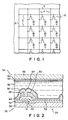
- Fig. 2 shows part of a matrix TFT array constituting a liquid crystal display device according to an embodiment of the present invention.
- a liquid crystal 36 is sealed between first and second substrates 32 and 34.
- first substrate 32 a large number of address lines (not shown) are formed, in a substantially parallel fashion, on a transparent substrate 38 made of, for example, glass.
- a large number of data lines (not shown) which are crossed with the address lines are provided with an insulating layer 42 formed therebetween.
- Gate electrodes 40 are formed integral with the address line at locations where data lines are provided over the corresponding gate lines.
- a semiconductor layer 44 is formed on the gate electrodes with the insulating layer 42 formed therebetween.
- a drain electrode 48 and source electrode 50 are formed on the semiconductor layer 44 in an opposed relation, noting that drain electrode 48 is formed integral with the data line. In this way, a TFT element 31 is constituted, serving as a non-linear active element.
- a transparent pixel electrode 52 is formed on the insulating film 42 in a manner to be connected to the source electrode 50.
- the semiconductor layer 44, drain electrode 48 and source electrode 50 are covered with a protective film 54. Further, an orientation film 56 is formed over the whole surface of the resultant structure.
- the second substrate 34 is formed opposite to the aforementioned first substrate 32.
- the second substrate 34 includes a transparent substrate 58 formed of, for example, glass, and transparent electrode 60 and orientation film 62 formed sequentially over the transparent substrate 58 in that order.
- a color filter is formed between the substrate 58 and the transparent electrode 60.
- the aforementioned TFT element 31 is provided by forming the gate electrode 40, insulating film 42, semiconductor layer 44 and drain and source electrodes 48 and 50 by repeating the film forming step and photoetching step a plurality of times.
- the central area 30 of the matrix TFT element is connected in an array shown in Fig. 3.
- each address line 40 in the central area 30 of the matrix TFT element is shorted by a common short-circuit line 70 and the outer end of each data line 48 is shorted by a common short-circuit line 72. Since these short-circuit lines 70 and 72 are shorted at each corner of the element, it is possible to prevent short-circuiting between the respective associated layers which results from static electricity involved.
- the address line 40 is formed integral with its outer end portion 74 used for signal supplying and its outer end portion 74′ used for examining, as shown in Figs. 3 and 4.
- the insulating film 42 is formed on that portion of the substrate where the end portions 74, 74′ of the address line is not present.
- the data lines 48, the terminals 76, 76′, the short-circuit lines 70, 72, and the terminals 78, 78′ connected to the short-circuit lines 70 and located over the address lines 40 are all formed, as an integral unit, using the same material.
- the terminal 74 of the address line 40 is connected to the terminal 78 of the short-circuit line 70 via a through-hole 80 which is formed in the insulating layer 42.
- the aforementioned manufacturing process is effected in connection with the following steps. That is, the short-circuit line 70 connected to the respective address line 40 and short-circuit line 72 connected to the respective data line 48 are formed and, at the same time, a short-circuit formation area 82 is formed in the neighborhood of a corner area where the short-circuit line 70 is connected to the short-circuit line 72.
- a short-circuit electrode 84 and a connection area 86 connected to one end of the short-circuit electrode 84 are formed on the substrate 38, the short-circuit electrode 84 and connection electrode 86 being formed of the same material as that of the address line 40.
- the insulating film 42 is formed over the short-circuit electrode 84. Then a short-circuit electrode 88 and connection electrode 90 are formed over the substrate 38 when the data line 48 is formed and, in this case, the electrode 88 and connection electrode 90 are formed of the same material as that of the data line 48.
- the short-circuit electrode 88 is connected to the short-circuit line 70 and the connection electrode 90 is connected to the short-circuit line 70 such that it is located over the connection electrode 86.
- the connection electrode 86 is connected by a through-hole 94 to the connection area 90 which is located over the connection electrode 86 with the insulating film 42 formed.
- the short-circuit electrode 84 connected to the short-circuit line 70 on the side of the address line 40 is located in an opposing relation to the short-circuit electrode 88 connected to the short-circuit line 72 on the side of the data line 48, the short-circuit electrode 84 being nonconductively formed relative to the short-circuit electrode 88 at the area 82 with the insulating film 42 formed therebetween.
- the TFT array is thus formed by the aforementioned method.
- the respective address lines 40 and data lines 48 are arranged in an interdigital fashion as shown in Fig. 6.
- the address lines 40 and data lines 48 are respectively connected to the corresponding short-circuit lines 70 and 72 in an alternate fashion, that is, in a fashion divided into odd- and even-numbered lines.
- the TFT array as shown in Fig. 6 is locally exposed to a laser beam to cut a corner area at an array of the short-circuit lines 70 and 72.
- the four sides of the array of the short-circuit lines 70 and 72 are called a, b, c and d, respectively.
- the corresponding ends located in an opposing relation to the four sides a, b, c and d of the array are called a′, b′, c′ and d′, respectively.
- electrical examination is made across a-a′, b-b′, c-c′ and d-d′ for the address lines 40 and the data lines 48.
- the short-circuit lines 70, 72 are short-circuited again.
- the short-circuit electrodes 84, 88 one at each surface of the insulating film 42 are locally exposed to a laser beam, and the electrodes 84, 88 are electrically connected.
- a connection resistance across the electrodes 84 and 88 reveals a better value of the order of a few ohms through a few hundreds of ohms upon measurement.
- the respective short-circuit lines 70, 72 in the TFT array are cut along a broken line 92 according to the present embodiment.
- Fig. 8 is a partial plan view showing an LC display device equipped with a matrix TFT array.
- the arrangement of the present embodiment is similar to the first embodiment except for added areas.
- the same reference numerals are employed to designate a part or an element corresponding to that in the first embodiment of the present invention.
- the second embodiment of the present invention is different from the preceding first embodiment in that two areas 82 and 82a are provided in the second embodiment in place of providing the short-circuit formation area 82 only at each corner of the short-circuit lines 70, 72.
- connection area A of short-circuit lines 70, 72 at each corner of a substrate is cut off and, in this state, examination is made in the same way as in the aforementioned embodiment.
- an area 82 to be made short-circuit at each corner is exposed to a laser beam, short-circuiting the respective short-circuit lines 70, 72.
- the resultant array substrate is transferred to an LC cell assembly process.
- a connection area B of the short-circuit lines 70, 72 at each corner is cut off the rest of the structure by a laser beam. Electrical examination is again made in that state.
- an area 82a to be made short-circuit is exposed to a laser beam, short-circuiting the short-circuit lines 70, 72. Then a cell sealing step, a liquid crystal filling step and a polarizing-plate attaching step are performed to complete a cell structure.
- the short-circuit lines 70, 72 are cut upon the assembly of the array substrate.
- the short-circuit line is opened by a laser beam and a short-circuit formation area is short-circuited by the laser beam.
- a short-circuit formation area is short-circuited by the laser beam.
- the LC display device is of such a type that an active element is located at a crosspoint where each of a plurality of address lines intersects with a corresponding one of a plurality of data lines over a substrate.
- the third embodiment is different from the first embodiment in that it is possible according to the third embodiment to short-circuit respective address lines and data lines and to use an examination method by which examination can be made for connection breakage and/or for a short-circuit between associated layers.
- respective address lines 40 are formed over a substrate in which case the address lines correspond to signal wiring layers in a row direction, that is, to signal wiring layers in a horizontal direction in a paper plane (drawing sheet).
- the address lines 40 are comprised of a greater number of linear sections 102 and connection sites 104.
- the linear sections 102 are all of equal length and are arranged in a parallel fashion.
- the connection sites 104 are connected to the ends of the alternate linear sections 102.
- the two adjacent connection sites 104 which are connected to the alternate linear sections 102 are connected to the alternately opposite ends.
- the address lines 40 are formed as a plurality of substantially U-shaped configurations with the two adjacent U-shape areas formed in an interdigital fashion.
- a terminal 106 is provided at the end of the respective address line 40. As shown in Fig. 10, an insulating film 108 is coated over the substrate on which the address line 40 is formed. A contact-through-hole 110 is opened at the terminal 106 of the respective address line 40.
- the data lines which correspond to signal wiring layers in a column direction (in a vertical direction in a paper sheet) are formed over the insulating film 108 in a manner to intersect with the linear section 102 of the address lines 40.
- a plurality of short-circuit lines 112 are provided each between the two terminals of the adjacent odd- and even-numbered address lines 40 as counted from the end of the address line 40.
- the short-circuit 112 is connected between the odd- and even-numbered terminals 106 and the adjacent odd- and even-numbered terminals 106 are connected respectively in a series array.
- the short-circuited spot between the respective address line and the respective data line is removed from the rest of the structure upon the assembly of an LC display device.
- the address lines 40 have been explained as being signal lines in the row direction, the same thing can also be said of the data lines which are used as signal lines in the column direction.
- the address and data lines may be electrically connected so as to prevent a dielectric breakdown resulting from static electricity. If the odd- and even-numbered address and data lines are connected in series array, it is possible to examine all the address lines and data lines, as a single line, respectively.
Landscapes
- Physics & Mathematics (AREA)
- Nonlinear Science (AREA)
- Optics & Photonics (AREA)
- General Physics & Mathematics (AREA)
- Chemical & Material Sciences (AREA)
- Crystallography & Structural Chemistry (AREA)
- Mathematical Physics (AREA)
- Engineering & Computer Science (AREA)
- Microelectronics & Electronic Packaging (AREA)
- Liquid Crystal (AREA)
- Devices For Indicating Variable Information By Combining Individual Elements (AREA)
- Thin Film Transistor (AREA)
- Testing Of Short-Circuits, Discontinuities, Leakage, Or Incorrect Line Connections (AREA)
- Testing Or Measuring Of Semiconductors Or The Like (AREA)
Applications Claiming Priority (2)
| Application Number | Priority Date | Filing Date | Title |
|---|---|---|---|
| JP322565/88 | 1988-12-21 | ||
| JP32256588A JP2610328B2 (ja) | 1988-12-21 | 1988-12-21 | 液晶表示素子の製造方法 |
Publications (3)
| Publication Number | Publication Date |
|---|---|
| EP0376165A2 true EP0376165A2 (de) | 1990-07-04 |
| EP0376165A3 EP0376165A3 (de) | 1991-07-24 |
| EP0376165B1 EP0376165B1 (de) | 1995-05-03 |
Family
ID=18145102
Family Applications (1)
| Application Number | Title | Priority Date | Filing Date |
|---|---|---|---|
| EP89123682A Expired - Lifetime EP0376165B1 (de) | 1988-12-21 | 1989-12-21 | Herstellungsmethode für eine Flüssigkristall-Anzeigevorrichtung |
Country Status (5)
| Country | Link |
|---|---|
| US (1) | US5019001A (de) |
| EP (1) | EP0376165B1 (de) |
| JP (1) | JP2610328B2 (de) |
| KR (1) | KR940006156B1 (de) |
| DE (1) | DE68922483T2 (de) |
Cited By (7)
| Publication number | Priority date | Publication date | Assignee | Title |
|---|---|---|---|---|
| EP0554062A1 (de) * | 1992-01-31 | 1993-08-04 | Canon Kabushiki Kaisha | Herstellung eines Transistorsubstrates mit Flüssigkristallzellen |
| EP0629895A3 (de) * | 1993-06-21 | 1995-04-26 | Ibm | Flüssigkristall-Anzeigevorrichtung. |
| EP0525980A3 (de) * | 1991-06-28 | 1995-09-06 | Sharp Kabushiki Kaisha | Verfahren zum Untersuchen eines Substrates mit aktiver Matrix |
| EP0793135A4 (de) * | 1994-11-08 | 1997-09-03 | ||
| EP0993038A1 (de) * | 1998-08-31 | 2000-04-12 | Canon Kabushiki Kaisha | TFT Matrix Paneel |
| US6229140B1 (en) | 1995-10-27 | 2001-05-08 | Canon Kabushiki Kaisha | Displacement information detection apparatus |
| EP1065554A4 (de) * | 1998-03-26 | 2002-03-20 | Matsushita Electric Industrial Co Ltd | Flüssigkristallanzeige und deren herstellungsverfahren |
Families Citing this family (22)
| Publication number | Priority date | Publication date | Assignee | Title |
|---|---|---|---|---|
| JPH02186321A (ja) * | 1989-01-13 | 1990-07-20 | Sharp Corp | アクティブマトリクス基板の検査方法 |
| JPH05313194A (ja) * | 1992-05-13 | 1993-11-26 | Nec Kagoshima Ltd | 薄膜トランジスタアレイ基板の製造方法 |
| GB9416899D0 (en) * | 1994-08-20 | 1994-10-12 | Philips Electronics Uk Ltd | Manufacture of electronic devices comprising thin-film circuitry |
| KR0145902B1 (ko) * | 1995-01-27 | 1998-09-15 | 김광호 | 박막트랜지스터 액정디스플레이 소자의 저항부 및 그 제조방법 |
| KR0166894B1 (ko) * | 1995-02-20 | 1999-03-30 | 구자홍 | 액정표시장치 |
| JP3254362B2 (ja) * | 1995-07-27 | 2002-02-04 | シャープ株式会社 | アクティブマトリクス基板 |
| US5668032A (en) * | 1995-07-31 | 1997-09-16 | Holmberg; Scott H. | Active matrix ESD protection and testing scheme |
| US6613650B1 (en) | 1995-07-31 | 2003-09-02 | Hyundai Electronics America | Active matrix ESD protection and testing scheme |
| JP3642876B2 (ja) * | 1995-08-04 | 2005-04-27 | 株式会社半導体エネルギー研究所 | プラズマを用いる半導体装置の作製方法及びプラズマを用いて作製された半導体装置 |
| JPH09251169A (ja) * | 1996-03-15 | 1997-09-22 | Toshiba Corp | 表示装置、アクティブマトリクス型表示装置およびその製造方法 |
| JP3838722B2 (ja) * | 1997-01-13 | 2006-10-25 | ローム株式会社 | 強制動作機能付き制御回路を有する半導体装置 |
| DE69840523D1 (de) * | 1997-01-13 | 2009-03-19 | Hyundai Electronics America | Verbesserter schutz fur aktiv-matrix-anzeigen vor elektrostatische entladungen sowie testschema |
| TW472165B (en) * | 1997-09-19 | 2002-01-11 | Toshiba Corp | Array substrate for display device, liquid crystal display device having array substrate and the manufacturing method of array substrate |
| US6215541B1 (en) * | 1997-11-20 | 2001-04-10 | Samsung Electronics Co., Ltd. | Liquid crystal displays and manufacturing methods thereof |
| KR100277501B1 (ko) * | 1998-02-16 | 2001-01-15 | 윤종용 | 액정표시장치및그제조방법 |
| US5976978A (en) * | 1997-12-22 | 1999-11-02 | General Electric Company | Process for repairing data transmission lines of imagers |
| JP4156115B2 (ja) * | 1998-12-25 | 2008-09-24 | シャープ株式会社 | マトリクス配線基板及び液晶表示装置用基板 |
| TW457690B (en) * | 1999-08-31 | 2001-10-01 | Fujitsu Ltd | Liquid crystal display |
| KR100390456B1 (ko) * | 2000-12-13 | 2003-07-07 | 엘지.필립스 엘시디 주식회사 | 액정 디스플레이 패널 및 그 제조방법 |
| JP5628139B2 (ja) * | 2011-10-18 | 2014-11-19 | シャープ株式会社 | 配線欠陥検査方法 |
| KR102296073B1 (ko) * | 2015-01-06 | 2021-08-31 | 삼성디스플레이 주식회사 | 액정 표시 장치 |
| JP2019117315A (ja) * | 2017-12-27 | 2019-07-18 | シャープ株式会社 | 表示装置、表示装置の製造方法、及び、表示装置の検査方法。 |
Family Cites Families (6)
| Publication number | Priority date | Publication date | Assignee | Title |
|---|---|---|---|---|
| DE2824308A1 (de) * | 1978-06-02 | 1979-12-13 | Siemens Ag | Verfahren zum einpraegen einer spannung mit einem elektronenstrahl |
| US4455739A (en) * | 1982-04-19 | 1984-06-26 | Texas Instruments Incorporated | Process protection for individual device gates on large area MIS devices |
| JPS634589U (de) * | 1986-06-25 | 1988-01-13 | ||
| KR920000601B1 (ko) * | 1986-10-13 | 1992-01-16 | 세미콘덕터 에너지 라보라터리 캄파니 리미티드 | 액정 장치 제조방법 |
| US4820222A (en) * | 1986-12-31 | 1989-04-11 | Alphasil, Inc. | Method of manufacturing flat panel backplanes including improved testing and yields thereof and displays made thereby |
| JP2583891B2 (ja) * | 1987-05-26 | 1997-02-19 | 松下電器産業株式会社 | アクテイブマトリクス表示装置の製造方法 |
-
1988
- 1988-12-21 JP JP32256588A patent/JP2610328B2/ja not_active Expired - Fee Related
-
1989
- 1989-12-20 US US07/453,802 patent/US5019001A/en not_active Expired - Lifetime
- 1989-12-21 KR KR1019890019431A patent/KR940006156B1/ko not_active Expired - Fee Related
- 1989-12-21 DE DE68922483T patent/DE68922483T2/de not_active Expired - Fee Related
- 1989-12-21 EP EP89123682A patent/EP0376165B1/de not_active Expired - Lifetime
Cited By (13)
| Publication number | Priority date | Publication date | Assignee | Title |
|---|---|---|---|---|
| EP0525980A3 (de) * | 1991-06-28 | 1995-09-06 | Sharp Kabushiki Kaisha | Verfahren zum Untersuchen eines Substrates mit aktiver Matrix |
| US5506516A (en) * | 1991-06-28 | 1996-04-09 | Sharp Kabushiki Kaisha | Method of inspecting an active matrix substrate |
| EP0554062A1 (de) * | 1992-01-31 | 1993-08-04 | Canon Kabushiki Kaisha | Herstellung eines Transistorsubstrates mit Flüssigkristallzellen |
| EP0629895A3 (de) * | 1993-06-21 | 1995-04-26 | Ibm | Flüssigkristall-Anzeigevorrichtung. |
| US6128050A (en) * | 1994-11-08 | 2000-10-03 | Citizen Watch Co., Ltd. | Liquid crystal display device with separated anode oxide electrode |
| EP0793135A4 (de) * | 1994-11-08 | 1997-09-03 | ||
| US6327443B1 (en) | 1994-11-08 | 2001-12-04 | Citizen Watch Co., Ltd. | Liquid crystal display device |
| US6388720B1 (en) | 1994-11-08 | 2002-05-14 | Citizen Watch Co., Ltd. | Liquid crystal display including signal electrodes connected to each other by first anode oxide electrode and auxiliary electrode connected to second anode oxide electrode |
| US6229140B1 (en) | 1995-10-27 | 2001-05-08 | Canon Kabushiki Kaisha | Displacement information detection apparatus |
| US6617572B2 (en) | 1995-10-27 | 2003-09-09 | Canon Kabushiki Kaisha | Displacement information detection apparatus |
| EP1065554A4 (de) * | 1998-03-26 | 2002-03-20 | Matsushita Electric Industrial Co Ltd | Flüssigkristallanzeige und deren herstellungsverfahren |
| US6522378B1 (en) | 1998-03-26 | 2003-02-18 | Matsushita Electric Industrial Co., Ltd. | Liquid crystal display and manufacture therefore |
| EP0993038A1 (de) * | 1998-08-31 | 2000-04-12 | Canon Kabushiki Kaisha | TFT Matrix Paneel |
Also Published As
| Publication number | Publication date |
|---|---|
| KR940006156B1 (ko) | 1994-07-08 |
| EP0376165B1 (de) | 1995-05-03 |
| US5019001A (en) | 1991-05-28 |
| KR900010455A (ko) | 1990-07-07 |
| JP2610328B2 (ja) | 1997-05-14 |
| DE68922483T2 (de) | 1995-09-07 |
| DE68922483D1 (de) | 1995-06-08 |
| EP0376165A3 (de) | 1991-07-24 |
| JPH02203380A (ja) | 1990-08-13 |
Similar Documents
| Publication | Publication Date | Title |
|---|---|---|
| EP0376165B1 (de) | Herstellungsmethode für eine Flüssigkristall-Anzeigevorrichtung | |
| KR100192193B1 (ko) | 다수의 션트 버스를 갖는 액정 표시 패널 | |
| EP0321073B1 (de) | Flüssigkristall Anzeigevorrichtung | |
| US6172410B1 (en) | Collective substrate of active-matrix substrates, manufacturing method thereof and inspecting method thereof | |
| US5068748A (en) | Active matrix liquid crystal display device having improved electrostatic discharge protection | |
| JP2715936B2 (ja) | 薄膜トランジスタ型液晶表示装置とその製造方法 | |
| EP1008177B1 (de) | Verbesserter schutz fur aktiv-matrix-anzeigen vor elektrostatische entladungen sowie testschema | |
| US6613650B1 (en) | Active matrix ESD protection and testing scheme | |
| KR100235169B1 (ko) | 액티브 매트릭스 기판 | |
| JP2687667B2 (ja) | マトリクス電極基板およびその製造方法 | |
| KR910006306B1 (ko) | 능동매트릭스 기판에 대한 전기적 시험방법 | |
| US6677171B1 (en) | Manufacturing method of collective substrate of active-matrix substrates, manufacturing method of active-matrix substrates, and inspecting method of collective substrates of active-matrix substrates | |
| KR100490040B1 (ko) | 두개이상의쇼팅바를갖는액정표시장치및그제조방법 | |
| JP3381681B2 (ja) | 液晶表示装置およびその断線補修方法 | |
| JP2820233B2 (ja) | 表示装置の検査装置および検査方法 | |
| KR100576629B1 (ko) | 액정표시장치의 tft어레이 기판 및 그 검사방법 | |
| JP3316929B2 (ja) | マトリックス配線基板 | |
| JP2834935B2 (ja) | アクティブマトリクス型表示素子及びその製造方法 | |
| JPH0772513A (ja) | アクティブマトリックス表示装置 | |
| JP2583891B2 (ja) | アクテイブマトリクス表示装置の製造方法 | |
| JPH05333370A (ja) | アクティブマトリクス型液晶表示素子 | |
| JPS62198826A (ja) | 液晶表示装置 | |
| US7049527B1 (en) | Conductor-pattern testing method, and electro-optical device | |
| JPWO2004109628A1 (ja) | アレイ基板の検査方法 | |
| JP3014915B2 (ja) | 多面取り薄膜トランジスタアレイ基板及びその検査方法 |
Legal Events
| Date | Code | Title | Description |
|---|---|---|---|
| PUAI | Public reference made under article 153(3) epc to a published international application that has entered the european phase |
Free format text: ORIGINAL CODE: 0009012 |
|
| 17P | Request for examination filed |
Effective date: 19900118 |
|
| AK | Designated contracting states |
Kind code of ref document: A2 Designated state(s): DE FR GB |
|
| PUAL | Search report despatched |
Free format text: ORIGINAL CODE: 0009013 |
|
| AK | Designated contracting states |
Kind code of ref document: A3 Designated state(s): DE FR GB |
|
| RHK1 | Main classification (correction) |
Ipc: G02F 1/136 |
|
| 17Q | First examination report despatched |
Effective date: 19930812 |
|
| GRAA | (expected) grant |
Free format text: ORIGINAL CODE: 0009210 |
|
| AK | Designated contracting states |
Kind code of ref document: B1 Designated state(s): DE FR GB |
|
| REF | Corresponds to: |
Ref document number: 68922483 Country of ref document: DE Date of ref document: 19950608 |
|
| ET | Fr: translation filed | ||
| PLBE | No opposition filed within time limit |
Free format text: ORIGINAL CODE: 0009261 |
|
| STAA | Information on the status of an ep patent application or granted ep patent |
Free format text: STATUS: NO OPPOSITION FILED WITHIN TIME LIMIT |
|
| 26N | No opposition filed | ||
| REG | Reference to a national code |
Ref country code: GB Ref legal event code: 746 Effective date: 19980929 |
|
| REG | Reference to a national code |
Ref country code: FR Ref legal event code: D6 |
|
| REG | Reference to a national code |
Ref country code: GB Ref legal event code: IF02 |
|
| PGFP | Annual fee paid to national office [announced via postgrant information from national office to epo] |
Ref country code: FR Payment date: 20051208 Year of fee payment: 17 |
|
| PGFP | Annual fee paid to national office [announced via postgrant information from national office to epo] |
Ref country code: DE Payment date: 20051215 Year of fee payment: 17 |
|
| PGFP | Annual fee paid to national office [announced via postgrant information from national office to epo] |
Ref country code: GB Payment date: 20051221 Year of fee payment: 17 |
|
| PG25 | Lapsed in a contracting state [announced via postgrant information from national office to epo] |
Ref country code: DE Free format text: LAPSE BECAUSE OF NON-PAYMENT OF DUE FEES Effective date: 20070703 |
|
| GBPC | Gb: european patent ceased through non-payment of renewal fee |
Effective date: 20061221 |
|
| REG | Reference to a national code |
Ref country code: FR Ref legal event code: ST Effective date: 20070831 |
|
| PG25 | Lapsed in a contracting state [announced via postgrant information from national office to epo] |
Ref country code: GB Free format text: LAPSE BECAUSE OF NON-PAYMENT OF DUE FEES Effective date: 20061221 |
|
| PG25 | Lapsed in a contracting state [announced via postgrant information from national office to epo] |
Ref country code: FR Free format text: LAPSE BECAUSE OF NON-PAYMENT OF DUE FEES Effective date: 20070102 |