EP0376332A2 - Dispositif d'affichage - Google Patents
Dispositif d'affichage Download PDFInfo
- Publication number
- EP0376332A2 EP0376332A2 EP89124108A EP89124108A EP0376332A2 EP 0376332 A2 EP0376332 A2 EP 0376332A2 EP 89124108 A EP89124108 A EP 89124108A EP 89124108 A EP89124108 A EP 89124108A EP 0376332 A2 EP0376332 A2 EP 0376332A2
- Authority
- EP
- European Patent Office
- Prior art keywords
- display apparatus
- cathode ray
- funnel
- ray tube
- fluorescent
- Prior art date
- Legal status (The legal status is an assumption and is not a legal conclusion. Google has not performed a legal analysis and makes no representation as to the accuracy of the status listed.)
- Granted
Links
Images


Classifications
-
- H—ELECTRICITY
- H04—ELECTRIC COMMUNICATION TECHNIQUE
- H04N—PICTORIAL COMMUNICATION, e.g. TELEVISION
- H04N9/00—Details of colour television systems
- H04N9/12—Picture reproducers
-
- H—ELECTRICITY
- H04—ELECTRIC COMMUNICATION TECHNIQUE
- H04N—PICTORIAL COMMUNICATION, e.g. TELEVISION
- H04N9/00—Details of colour television systems
- H04N9/12—Picture reproducers
- H04N9/16—Picture reproducers using cathode ray tubes
- H04N9/22—Picture reproducers using cathode ray tubes using the same beam for more than one primary colour information
Definitions
- the present invention relates generally to display devices (so-called display cells) for use with a large screen display apparatus and particularly to a display device for use with an indoor-type large screen display apparatus employing a cathode ray tube.
- a large screen display apparatus is constructed by assembling a plurality of existing television receivers in the vertical and horizontal directions as shown in Fig. 1 or the large screen display apparatus is constructed by assembling a plurality of liquid crystal display devices similarly as described above.
- an 8-element display device 35 or the like is proposed (see Japanese Patent Laid-Open Gazette No. 60-191703).
- the 8-element display device 35 a plurality of, for example, 8 sets of fluorescent trios 34, each formed of green, red and blue three primary color fluorescent layers G, R and B forming a pixel are provided within a glass tube envelope 33 formed of a front panel 31, a rear panel (not shown) and a side plate 32.
- the display devices 35 are arranged in a two-dimensional manner, thereby forming a large-sized display apparatus as shown in Fig. 1 or 2. This type of large-sized display apparatus provides sufficient brightness so that it can reproduce a clear visual image even outdoors.
- a matrix display in which a cathode ray tube 36 is utilized as a display cell as shown in Fig. 3.
- a connected portion between the adjacent cathode ray tubes 41 and 41 causes a cross bar 42, which deteriorates the quality of image considerably.
- a panel-funnel connected portion needs a proper thickness t1 from a mechanical strength and dielectric strength standpoint.
- the limit of the thickness of, for example, a 4-inch cathode ray tube falls in a range of from 2.5 mm to 3 mm.
- a useless portion l between the adjacent cathode ray tubes 41 and 41 is large and this large useless portion l becomes a cross bar, resulting in the image quality to be deteriorated.
- reference letter m represents the effective portion.
- a viewfinder for a video camera utilizes a cathode ray tube 54 wherein a tube envelope 53 is formed of a flat panel 51 of flat-shaped glass and a funnel portion 52.
- reference letter 55 designates a fluorescent screen, and 56 an electron gun.
- a viewfinder of about 0.7-inch is applied with a high voltage of less than 5 kV, for example, 2 kV so that a thickness t2 of the funnel portion 52 of the tube envelope thereof is as sufficient as about 1 mm from a mechanical strength and dielectric strength standpoint.
- this type of viewfinder is formed as 4-inch type or the like, then this 4-inch type viewfinder needs large mechanical strength and dielectric strength with the result that the funnel of about 1mm thick can not be employed.
- each of the fluorescent trios 34 is formed as a rectangular strip configuration and the longitudinal direction of the fluorescent trios 34 is aligned in the vertical direction of the display screen so that the following problems arise.
- the fluorescent trio series 34l and 34r existing at respective sides of the picture screen when the viewer watches the picture screen from a relatively lateral direction relative to the display picture screen (this situation is inavoidable when many viewers watch the same display screen because a space in which the display apparatus is located indoors is small), of the fluorescent trio series 34l and 34r existing at respective sides of the picture screen, the fluorescent series located at the endmost of the picture screen are hidden by a frame 37, so that the fluorescent trio series 34l and 34r existing at the respective sides can not function to display a visual image.
- the leftmost fluorescent trio series 34l in the case of a viewer Hl who watches the picture screen from the left-hand side, of the leftmost fluorescent trio series (area shown by a one-dot chain line) 34l, the leftmost fluorescent series G is hidden by the frame 37, whereby the visual image displayed by the fluorescent trio series 34l does not look natural color but looks predetermined color (magenta, which should be originally white) for the viewer Hl.
- the above-mentioned fluorescent trio series 34l does not function as a fluorescent trio for displaying the visual image. This is also true for a viewer Hr who watches the picture screen from the right-hand side. That is, the fluorescent trio series 34r located in the rightmost position of the picture screen look predetermined color (in that case, yellow), and can not function as the fluorescent trio by which the visual image is displayed.
- a visual field A1 of the visual image distant by a predetermined distance n of the display apparatus must be considered in practice excepting the fluorescent trio series 34l and 34r at the respective side ends so that the visual field A1 is reduced to a visual field A2 as shown in Fig. 6. Therefore, the function (to enable to many viewers to watch the same large screen) of the large screen display apparatus can not be demonstrated sufficiently.
- the glass tube envelope 33 has to have a sufficient thickness from a mechanical strength and dielectric strength standpoint, and thus a resolution can not be sufficiently increased by reducing the pitch of the fluorescent trio 34.
- a display panel formed by arranging a plurality of picture cells in a XY matrix form.
- a plurality of slit-shaped self luminous pixel elements are formed on a display screen of a tube envelope in a predetermined pitch so that their longitudinal directions are directed in the horizontal direction of the display screen.
- a phenomenon in which one of flurorescent trios located at the side end portions is hidden by the frame when the user watches the display screen from the lateral direction is avoided. Therefore, a range of visual field relative to a predetermined distance can be enlarged and the function of large screen can be sufficiently demonstrated.
- a cathode ray tube for use with a large display screen, in which a stepped portion is provided on the peripheral edge portion of a flat panel having a fluorescent screen formed on its inner surface, and a funnel portion is bonded to this stepped portion.
- the thickness the funnel at its bonding portion in which the funnel is bonded to the panel is reduced more than the thickness of other portion of the funnel.
- a cathode ray tube in which the stepped portion of the flat panel on its peripheral edge portion is provided outside of a line connecting the fluorescent element adjacent to the stepped portion and the end portion of the flat panel.
- the thickness of the funnel at its bonding portion in which the funnel and the panel are bonded is reduced, whereby the screen side wall portion of the tube envelope can be reduced in thickness.
- Fig. 7 is a side view of a section of a cathode ray tube (cathode ray tube suitably used as large screen display element), and to which the present invention can be advantageously applied.
- Fig. 8 is a front view of Fig. 7, and
- Fig. 9 is a side view of a section of a main component of the cathode ray tube of Fig. 7.
- a tube envelope 1 is comprised of a glass flat panel 2 and a glass funnel portion 3 which is formed as one body with the necked-down portion.
- each of the fluorescent trios 4 is formed of blue light-emission, red light-emission and green-light emission fluorescent layers B, R and G, each having a length L and a width W .
- These fluorescent trios 4 are arranged with a predetermined pitch P and the longitudinal directions of the fluorescent layers B, R and G are aligned in the horizontal direction relative to the display screen 9, i.e., in the X direction.
- Light absorption layers are formed on the surface other than the fluorescent layers B, R and G.
- a stepped-portion 10 is formed on the inner peripheral edge portion of the flat panel 2 formed of a flat-shaped glass, and the end portion of the funnel 3 is bonded to the stepped-portion 10.
- the outer peripheral surface 3a near the area to be bonded to the flat panel 2 i.e., the picture screen side wall portion is formed in flush with the side surface 2a of the panel 2.
- the outer peripheral surface 3a is formed in the direction vertical to the plane of the flat panel 2.
- the inside surface 3b of the funnel 3 at the picture screen side wall portion is tapered so that the thickness of the funnel 3 is gradually reduced toward the bonded end thereof.
- its inner side wall 10a is tapered in correspondence with the tapered inside surface 3b of the funnel 3.
- the stepped portion 10 is formed outside a line n connecting the fluorescent material adjacent to the stepped portion 10, i.e., the fluorescent material located at the rightmost position of the fluorescent screen 5 and the end portion of the flat panel 2.
- the fluorescent trios 4 may be produced by either a printing method or a so-called slurry method.
- an electron gun 6 may be of a type from which is emitted a single electron beam e .
- the electron beam is deflected in the vertical and horizontal directions by a deflection yoke 7 so that it impinges upon the blue fluorescent layer B, the red fluorescent layer R and the green fluorescent layer G of one fluorescent trio 4.
- the shape of laser beam may be a laterally-extended beam shape (e.g., ellipse) in accordance with the shape of the fluorescent layer.
- the longitudinal directions of the fluorescent trios 4 are aligned in the X direction, unlike the prior-art scanning method, i.e., the method in which the electron beam is scanned in the horizontal direction (X direction) so as to impinge upon the fluorescent layers B, R and G, the electron beam is scanned in the vertical direction (Y direction) so as to impinge upon the fluorescent layers B, R and G.
- X direction horizontal direction
- Y direction vertical direction
- a large screen display apparatus 11 By arranging a number of the thus arranged cathode ray tubes in a two-dimensional fashion or in a XY matrix form, it is possible to form a large screen display apparatus 11 in which a spacing between the adjacent cathode ray tubes is represented by d (see Fig. 12), as shown in Figs. 10 and 11.
- cathode ray tubes are arranged in the longitudinal direction, and 40 cathode ray tube are arranged in the lateral direction, i.e., 1200 cathode ray tubes are arranged, thereby constructing the large screen display apparatus 11.
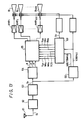
- a television signal Si received at an antenna 61 is supplied through a tuner 62 to a video detector 63, in which it is demodulated to provide a composite video signal S1.
- This video signal S1 is supplied to a luminance/chroma signal processing circuit (Y/C processor circuit) 64, in which it is processed to provide blue, red and green three primary color signals R, G and B.
- the three primary color signals B, R and G are supplied to a succeeding image processor circuit 65.
- the antenna circuit 61, the tuner 62, the video detector 63 and the Y/C processor circuit 64 are those employed for receiving a standard television signal. These elements do not have any special features and therefore need not be described in detail.
- the composite video signal S1 from the video detector 63 is supplied to a synchronizing separating circuit 66, in which it is separated to provide a horizontal synchronizing signal H and a vertical synchronizing signal V.
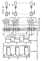
- the image processor circuit 65 is mainly formed of a field memory circuit 67 as shown in Fig. 14.
- the field memory circuit 67 is adapted to store the three primary color signals B, R and G inputted thereto from the Y/C processor circuit 64 in units of fields. More specifically, as shown in Fig. 14, the field memory circuit 67 is provided with write field memories WB, WR and WG and read field memories RB, RR and RG for the three primary color signals B, R and G. That is, the field memory circuit 67 is provided with 6 field memories.
- the timing control circuit 68 generates various timing signals, and the three primary color signals R, G and B are sampled by the above described sampling signal fsp. Simultaneously, other timing signals derived from the timing control circuit 68, i.e., write address signals WAX and WAY are used to control the write field memories WB, WR and WG so that the write field memories WB, WR and WG correctly write the three primary color signals B, R and G, in that order.
- write address signals WAX and WAY are used to control the write field memories WB, WR and WG so that the write field memories WB, WR and WG correctly write the three primary color signals B, R and G, in that order.
- the frequency of the sampling signal fsp could be selected to be a frequency corresponding to 76800 sampling operations, because the standard field memory for visual image has a sampling frequency more than 76800, it is practical that the field memory for visual image is used as it is wherein the read address for the field memory is controlled so as to obtain necessary information.
- the signals, written in the write field memories WR, WB and WG line by line as set forth above, are transferred to small memories M1, 22, .., M1200 that are provided to drive the cathode ray tubes during the next field scanning period, for example, the vertical blanking period.
- the timing control circuit 68 delivers a transfer control signal TCS.
- the line of the control signal TCS is represented by a single line in Fig. 13
- the line of the control signal TCS is formed of lines of address signals used to read the write field memories WB, WR and WG, address signals to write data in the small memories M1, M2, ... M1200 for driving the respective cathode ray tubes, control signals for driving selector circuits SB, SR and SG provided between the field memory 67 and the small memories M1, M2, ..., M1200 or the like as shown in Fig. 14.
- Each of the small memories M1, M2, ..., M1200 includes write and read special memories, i.e., 6 special memories for the three primary color signals B, R and G similarly to the above-mentioned field memory 67.
- Fig. 15A two read and write field memories FB1 and FB2 for one primary color signal, for example, blue signal B are used and switches S11 and S21 are changed in oposition, whereby the field memories FB1 and FB2 are cyclically selected as the read memory or the write memory.
- the switches S11 and S21 are respectively connected to their fixed contacts a and d .
- data of the preceding field may be read from the other field memory FB2 and transferred to the small memories M1, M2, ..., M1200.
- Data of the second field is written in the vacant other field memory FB2 by connecting the switch S11 to its fixed contact b .
- the data of the first field is read to the small memories M1, M2, ..., M1200 by connecting the switch S21 to its fixed contact c .
- Other field memories FR1, FR2 and FG1, FG2 are operated similarly, and read and write thereof are respectively selected by switches S12, S22 and S13, S23.
- the switches S11, S12, S13, S21, S22 and S23 are simultaneously operated thereby effecting the write and read at the same time
- the following variant is also possible. That is, the vertical blanking period in the input scanning is utilized such that during the vertical blanking period, the switches S11, S12, S13 and the switches S21, S22, S23 are operated with different phases, whereby informations are read from one memories first and then informations read are written in the other memories.
- Each of the small memories M1, M2, ..., M1200 includes two read and write memories MB1, MB2, MR1, MR2, MG1, MG2 for the three primary color signals similarly to the above-mentioned field memory circuit 67.
- the read and write of these memories MB1, MB2, MR1, MR2 and MG1, MG2 can be selected by switches S31, S32, S33 and switches S41, S42, S43.
- the memories MB1, MR1 and MG1 are each controlled so as to store 64 informations.
- the image signals transferred to the special memories MB1, MR1 and MG1 are read as follows. More specifically, read address signals RAx and RAy from the timing control circuit 68 are supplied to the special memories MB1, MR1 and MG1 which are provided within the small memories M1 to M1200. At that time, according to this embodiment, by controlling the read address signals RAx and RAy, the order of read operation is made in accordance with the vertical direction of the picture screen so that the image signals stored in the field memories FB1, FR1 and FG1 and the special memories MB1, MR1 and MG1 line by line and in the horizontal direction are read therefrom in the longitudinal direction (vertical direction) upon reading as shown in Fig. 16A.
- the signals read from the special memories MB1, MR1 and MG1 as described above are converted to serial signals by a switching signal fsw supplied from the timing control circuit 68.
- a switching signal fsw supplied from the timing control circuit 68.
- a memory switch sb for blue signal is turned ON to permit the blue signal B memory MB1 or MB2 to derive a signal
- a memory switch sr for red signal is turned ON to permit the red signal R memory MR1 or MR2 to derive a signal
- a memory switch sg for green signals is turned ON to permit the green signal G memory MG1 or MG2 to derive a signal.
- 1200 serial signals are supplied through amplifiers AMP1 to AMP1200 to the cathode ray tubes 81 to 81200
- switching signal fsw is represented by a single control line in Fig. 13, in practice, three control lines f SW1 , F SW2 and F SW3 are provided as shown in Fig. 14 and these three control lines f SW1 , F SW2 and F SW3 are supplied with switching signals whose phases are different as shown in Fig. 17.
- the deflection method is also changed because the reading direction is changed to the vertical direction as described above.
- the horizontal deflections of the respective cathode ray tubes 8 are carried out at the same time.
- reference letter H CM represents the horizontally-deflected waveform.
- the vertical deflecting signal Sv obtained from the timing control circuit 68 is carried out simultaneously.
- reference letter V CM represents the vertically-deflected waveform.
- the image display apparatus of the invention is mainly used indoors so that it is provided with 1200 cathode ray tubes.
- the input signal is the interlaced-scanning signal
- the same portion is impinged in the odd field and the even field.
- the large screen display apparatus is formed of 1200 cathode ray tubes of a small number
- the pairs of the field memories and the special or exclusive memories are provided for the three primary color signals R, G and B in the above-mentioned embodiment.
- one field memory and one exclusive memory may be instantaneously switched upon read and/or write operation, thereby reducing the number of memories by half.
- the stepped portion 10 is provided at the peripheral edge portion of the inner surface of the flat panel 2 and the funnel 3 is bonded to the stepped portion 10 through the frit glass 12, thereby forming the tube envelope 1. Therefore, the mechanical strength at the bonded portion can be increased, and the length of the bonded portion by the frit glass 12 can be increased, thereby obtaining sufficient dielectric strength. Consequently, the thickness t3 of the funnel 3 at the screen side wall portion can be reduced, i.e., can be reduced to become less than 1/2 of the thickness t1 according to the prior art of Fig. 4.
- the funnel 3 is bonded to the panel 2 at its stepped portion 10 so that, as compared with the tube envelope in which the funnel 3 is bonded to the side surface of the panel 2 in order to increse strength and dielectric strength, a visual field angle ⁇ 1 ( ⁇ 1 > ⁇ 2) can be increased.
- a visual field angle ⁇ 1 ⁇ 1 > ⁇ 2
- the loss of visual field angle due to the thickness t3 of the funnel 3 in Fig. 18 can be removed.
- the fluorescent layer located at the side most end of the fluorescent screen 5 is provided outside the line n connecting the end portions of the panel and screen 5, and therefore the visual field angle ⁇ 1 can be increased more.
- the cathode ray tube 8 is formed such that the fluorescent trios 4 of slit-configuration having a predetermined pitch P are formed on the display screen with their longitudinal directions directed in the horizontal direction (X direction).
- the fluorescent trios 4 are provided between the adjacent cathode ray tubes 8 in the above-mentioned pitch P , and the bonded portion between the adjacent cathode ray tubes 8 act as the light absorption area of the fluorescent screen 5, thereby providing an image of high quality in which the bonded portion is inconspicuous.
- the thickness t3 of the funnel 3 at its screen side wall portion can be reduced to be less than 1/2 of the thickness t1 of the prior art so that the pitch P of the fluorescent trios 4 can be reduced more. Therefore, it is possible to obtain a large screen display apparatus of high resolution.
- the outer peripheral surface 3a of the funnel 3 at its screen side wall portion of each of the cathode ray tubes 8 is formed as the flat surface, it is possible to arrange with ease the cathode ray tubes 8 in a XY matrix-fashion.
- the panel 2 of the embodiment of the invention is formed as the flat panel so that the flurorescent screen 5 can be made thereon by the printing-process, thus the manufacturing cost of the large screen display apparatus can be reduced considerably. Furthermore, when the large screen display apparatus is constructed as described above, the large screen, formed of a number of cathode ray tubes, can be seen as one picture screen.
Landscapes
- Engineering & Computer Science (AREA)
- Multimedia (AREA)
- Signal Processing (AREA)
- Vessels, Lead-In Wires, Accessory Apparatuses For Cathode-Ray Tubes (AREA)
- Cathode-Ray Tubes And Fluorescent Screens For Display (AREA)
Applications Claiming Priority (4)
| Application Number | Priority Date | Filing Date | Title |
|---|---|---|---|
| JP63331505A JPH02178692A (ja) | 1988-12-29 | 1988-12-29 | 大画面用表示素子 |
| JP331505/88 | 1988-12-29 | ||
| JP1021183A JPH02201849A (ja) | 1989-01-31 | 1989-01-31 | 陰極線管及び大画面表示装置 |
| JP21183/89 | 1989-01-31 |
Publications (3)
| Publication Number | Publication Date |
|---|---|
| EP0376332A2 true EP0376332A2 (fr) | 1990-07-04 |
| EP0376332A3 EP0376332A3 (fr) | 1991-07-03 |
| EP0376332B1 EP0376332B1 (fr) | 1995-03-08 |
Family
ID=26358222
Family Applications (1)
| Application Number | Title | Priority Date | Filing Date |
|---|---|---|---|
| EP89124108A Expired - Lifetime EP0376332B1 (fr) | 1988-12-29 | 1989-12-28 | Dispositif d'affichage |
Country Status (4)
| Country | Link |
|---|---|
| US (1) | US5057739A (fr) |
| EP (1) | EP0376332B1 (fr) |
| KR (1) | KR0169962B1 (fr) |
| DE (1) | DE68921592T2 (fr) |
Cited By (8)
| Publication number | Priority date | Publication date | Assignee | Title |
|---|---|---|---|---|
| EP0387911A3 (fr) * | 1989-03-17 | 1992-10-14 | Sony Corporation | Dispositif d'affichage vidéo du type CRT-matriciel |
| WO1994017637A1 (fr) * | 1993-01-22 | 1994-08-04 | C.D. Interactive Ltd. | Systeme d'affichage video |
| US5361078A (en) * | 1990-02-16 | 1994-11-01 | Nadimelia Limited | Multiple screen graphics display |
| EP0680067A3 (fr) * | 1994-04-28 | 1998-12-02 | Matsushita Electronics Corporation | Appareil d'affichage à décharge gazeuse et méthode pour commande un tel appareil |
| US5897192A (en) * | 1994-04-18 | 1999-04-27 | Seufert; Heinz | Rear projection module |
| US6072279A (en) * | 1994-04-28 | 2000-06-06 | Matsushita Electronics Corporation | Gas discharge display apparatus and method for driving the same |
| US6243060B1 (en) | 1997-02-20 | 2001-06-05 | Sony Corporation | Image display and its pixel arrangement method |
| WO2015128408A1 (fr) * | 2014-02-28 | 2015-09-03 | Barco N.V. | Affichages en pavés sans coupure |
Families Citing this family (22)
| Publication number | Priority date | Publication date | Assignee | Title |
|---|---|---|---|---|
| JP2804392B2 (ja) * | 1991-07-16 | 1998-09-24 | 三菱電機株式会社 | 発光素子及びその製造方法 |
| JP3426340B2 (ja) * | 1994-05-30 | 2003-07-14 | ノリタケ伊勢電子株式会社 | 光源用表示管およびその製造方法 |
| US6356278B1 (en) | 1998-10-07 | 2002-03-12 | Microsoft Corporation | Methods and systems for asymmeteric supersampling rasterization of image data |
| US6278434B1 (en) | 1998-10-07 | 2001-08-21 | Microsoft Corporation | Non-square scaling of image data to be mapped to pixel sub-components |
| WO2000021069A1 (fr) | 1998-10-07 | 2000-04-13 | Microsoft Corporation | Projection d'echantillons de donnees d'images couleur d'avant-plan/arriere-plan sur des sous-composants de pixels |
| US6597360B1 (en) | 1998-10-07 | 2003-07-22 | Microsoft Corporation | Automatic optimization of the position of stems of text characters |
| US6236390B1 (en) | 1998-10-07 | 2001-05-22 | Microsoft Corporation | Methods and apparatus for positioning displayed characters |
| US6307566B1 (en) | 1998-10-07 | 2001-10-23 | Microsoft Corporation | Methods and apparatus for performing image rendering and rasterization operations |
| US6188385B1 (en) * | 1998-10-07 | 2001-02-13 | Microsoft Corporation | Method and apparatus for displaying images such as text |
| US6973210B1 (en) | 1999-01-12 | 2005-12-06 | Microsoft Corporation | Filtering image data to obtain samples mapped to pixel sub-components of a display device |
| AU2504800A (en) * | 1999-01-12 | 2000-08-01 | Microsoft Corporation | Filtering image data to obtain samples mapped to pixel sub-components of a display device |
| US6393145B2 (en) | 1999-01-12 | 2002-05-21 | Microsoft Corporation | Methods apparatus and data structures for enhancing the resolution of images to be rendered on patterned display devices |
| US6750875B1 (en) | 1999-02-01 | 2004-06-15 | Microsoft Corporation | Compression of image data associated with two-dimensional arrays of pixel sub-components |
| US6674436B1 (en) | 1999-02-01 | 2004-01-06 | Microsoft Corporation | Methods and apparatus for improving the quality of displayed images through the use of display device and display condition information |
| US7134091B2 (en) * | 1999-02-01 | 2006-11-07 | Microsoft Corporation | Quality of displayed images with user preference information |
| US6342890B1 (en) | 1999-03-19 | 2002-01-29 | Microsoft Corporation | Methods, apparatus, and data structures for accessing sub-pixel data having left side bearing information |
| US6342896B1 (en) | 1999-03-19 | 2002-01-29 | Microsoft Corporation | Methods and apparatus for efficiently implementing and modifying foreground and background color selections |
| US6339426B1 (en) | 1999-04-29 | 2002-01-15 | Microsoft Corporation | Methods, apparatus and data structures for overscaling or oversampling character feature information in a system for rendering text on horizontally striped displays |
| US6738526B1 (en) | 1999-07-30 | 2004-05-18 | Microsoft Corporation | Method and apparatus for filtering and caching data representing images |
| US6282327B1 (en) | 1999-07-30 | 2001-08-28 | Microsoft Corporation | Maintaining advance widths of existing characters that have been resolution enhanced |
| US6226017B1 (en) | 1999-07-30 | 2001-05-01 | Microsoft Corporation | Methods and apparatus for improving read/modify/write operations |
| KR100885016B1 (ko) * | 2002-08-20 | 2009-02-20 | 삼성전자주식회사 | 액정 표시 장치 |
Family Cites Families (9)
| Publication number | Priority date | Publication date | Assignee | Title |
|---|---|---|---|---|
| US2337980A (en) * | 1941-04-26 | 1943-12-28 | Du Mont Allen B Lab Inc | System for color television receivers |
| US4070596A (en) * | 1971-08-27 | 1978-01-24 | Tokyo Shibaura Electric Co., Ltd. | In-line plural beams cathode ray tube having color phosphor element strips spaced from each other by intervening light absorbing areas and slit-shaped aperture mask |
| JPS5344309B2 (fr) * | 1973-07-28 | 1978-11-28 | ||
| US4204222A (en) * | 1978-06-19 | 1980-05-20 | Antoine Zacharie | High output LED matrix color TV screen with vertical triad and tricolor faceplate |
| US4810928A (en) * | 1982-12-06 | 1989-03-07 | Hitachi, Ltd. | Cathode-ray tube for constituting large picture display apparatus |
| FR2549671B1 (fr) * | 1983-07-22 | 1987-05-22 | Thomson Csf | Dispositif d'affichage d'une image de television de grandes dimensions et recepteur de television comportant un tel dispositif |
| US4590404A (en) * | 1984-03-30 | 1986-05-20 | Rca Corporation | Cathode-ray tube having a faceplate with decreasing center-to-edge thickness |
| JPH061674B2 (ja) * | 1984-12-04 | 1994-01-05 | ソニー株式会社 | 螢光表示管 |
| US4900977A (en) * | 1988-04-04 | 1990-02-13 | Corning Incorporated | Support system for flat CRT tension mask |
-
1989
- 1989-12-28 DE DE68921592T patent/DE68921592T2/de not_active Expired - Fee Related
- 1989-12-28 US US07/458,456 patent/US5057739A/en not_active Expired - Fee Related
- 1989-12-28 EP EP89124108A patent/EP0376332B1/fr not_active Expired - Lifetime
- 1989-12-28 KR KR1019890019826A patent/KR0169962B1/ko not_active Expired - Fee Related
Cited By (12)
| Publication number | Priority date | Publication date | Assignee | Title |
|---|---|---|---|---|
| EP0387911A3 (fr) * | 1989-03-17 | 1992-10-14 | Sony Corporation | Dispositif d'affichage vidéo du type CRT-matriciel |
| US5361078A (en) * | 1990-02-16 | 1994-11-01 | Nadimelia Limited | Multiple screen graphics display |
| WO1994017637A1 (fr) * | 1993-01-22 | 1994-08-04 | C.D. Interactive Ltd. | Systeme d'affichage video |
| US5897192A (en) * | 1994-04-18 | 1999-04-27 | Seufert; Heinz | Rear projection module |
| EP0680067A3 (fr) * | 1994-04-28 | 1998-12-02 | Matsushita Electronics Corporation | Appareil d'affichage à décharge gazeuse et méthode pour commande un tel appareil |
| US6072279A (en) * | 1994-04-28 | 2000-06-06 | Matsushita Electronics Corporation | Gas discharge display apparatus and method for driving the same |
| US6118220A (en) * | 1994-04-28 | 2000-09-12 | Matsushita Electronics Corporation | Gas discharge display apparatus and method for driving the same |
| US6150766A (en) * | 1994-04-28 | 2000-11-21 | Matsushita Electric Industrial Co., Ltd. | Gas discharge display apparatus and method for driving the same |
| US6243060B1 (en) | 1997-02-20 | 2001-06-05 | Sony Corporation | Image display and its pixel arrangement method |
| WO2015128408A1 (fr) * | 2014-02-28 | 2015-09-03 | Barco N.V. | Affichages en pavés sans coupure |
| BE1024100B1 (nl) * | 2014-02-28 | 2017-11-16 | Barco Nv. | Naadloze tiled display |
| US9936177B2 (en) | 2014-02-28 | 2018-04-03 | Barco N.V. | Seamless tiled displays |
Also Published As
| Publication number | Publication date |
|---|---|
| KR0169962B1 (ko) | 1999-03-20 |
| DE68921592T2 (de) | 1995-10-19 |
| EP0376332A3 (fr) | 1991-07-03 |
| EP0376332B1 (fr) | 1995-03-08 |
| US5057739A (en) | 1991-10-15 |
| KR900010625A (ko) | 1990-07-09 |
| DE68921592D1 (de) | 1995-04-13 |
Similar Documents
| Publication | Publication Date | Title |
|---|---|---|
| EP0376332B1 (fr) | Dispositif d'affichage | |
| CA1231172A (fr) | Decodeur pour extraire d'un signal de television a haute definition un signal d'image a rapport largeur/hauteur de 4:3 | |
| US5534940A (en) | Apparatus and method for driving a liquid crystal display utilizing various television system formats | |
| US4758884A (en) | Electronically switched field sequential color video display having parallel color inputs | |
| GB684664A (en) | Colour television image reproduction | |
| EP0138021B1 (fr) | Projecteur à rayons multiples | |
| US2965704A (en) | Colour television and like systems | |
| EP0454455B1 (fr) | Appareil de télévision | |
| US5138435A (en) | Crt-matrix display with indexing and stair step vertical deflection waveform. | |
| EP0490682B1 (fr) | Petit appareil d'affichage en couleur à haute résolution | |
| US4941049A (en) | Television system using reversing scan which minimizes ghost visibility | |
| EP0766457A2 (fr) | Dispositif de circuit de balayage amélioré pour un récepteur de télévision | |
| GB1588459A (en) | Line scan converter for an image display device | |
| EP0083398B1 (fr) | Appareil pour obtenir des images à trame multicolorée utilisant un tube cathodique du type à pénétration d'électrons | |
| US4527100A (en) | Flat color picture reproduction or video display device | |
| US5621276A (en) | Cathode ray tube | |
| JPH0614689B2 (ja) | 映像表示装置 | |
| JPH05241525A (ja) | カラー表示装置 | |
| CA1339621C (fr) | Systeme d'affichage video | |
| JPH0537877A (ja) | インデツクス管 | |
| JPH02178692A (ja) | 大画面用表示素子 | |
| JPH04233879A (ja) | プロジェクションテレビ | |
| JP2000041265A (ja) | 往復偏向式映像信号表示装置 | |
| JPH0195686A (ja) | 映像表示システム | |
| JPH08322056A (ja) | 表示装置 |
Legal Events
| Date | Code | Title | Description |
|---|---|---|---|
| PUAI | Public reference made under article 153(3) epc to a published international application that has entered the european phase |
Free format text: ORIGINAL CODE: 0009012 |
|
| AK | Designated contracting states |
Kind code of ref document: A2 Designated state(s): DE FR GB |
|
| 17P | Request for examination filed |
Effective date: 19901220 |
|
| PUAL | Search report despatched |
Free format text: ORIGINAL CODE: 0009013 |
|
| AK | Designated contracting states |
Kind code of ref document: A3 Designated state(s): DE FR GB |
|
| 17Q | First examination report despatched |
Effective date: 19931007 |
|
| GRAA | (expected) grant |
Free format text: ORIGINAL CODE: 0009210 |
|
| AK | Designated contracting states |
Kind code of ref document: B1 Designated state(s): DE FR GB |
|
| REF | Corresponds to: |
Ref document number: 68921592 Country of ref document: DE Date of ref document: 19950413 |
|
| ET | Fr: translation filed | ||
| PGFP | Annual fee paid to national office [announced via postgrant information from national office to epo] |
Ref country code: FR Payment date: 19951212 Year of fee payment: 7 |
|
| PGFP | Annual fee paid to national office [announced via postgrant information from national office to epo] |
Ref country code: GB Payment date: 19951219 Year of fee payment: 7 |
|
| PGFP | Annual fee paid to national office [announced via postgrant information from national office to epo] |
Ref country code: DE Payment date: 19951222 Year of fee payment: 7 |
|
| PLBE | No opposition filed within time limit |
Free format text: ORIGINAL CODE: 0009261 |
|
| STAA | Information on the status of an ep patent application or granted ep patent |
Free format text: STATUS: NO OPPOSITION FILED WITHIN TIME LIMIT |
|
| 26N | No opposition filed | ||
| PG25 | Lapsed in a contracting state [announced via postgrant information from national office to epo] |
Ref country code: GB Effective date: 19961228 |
|
| GBPC | Gb: european patent ceased through non-payment of renewal fee |
Effective date: 19961228 |
|
| PG25 | Lapsed in a contracting state [announced via postgrant information from national office to epo] |
Ref country code: FR Effective date: 19970829 |
|
| PG25 | Lapsed in a contracting state [announced via postgrant information from national office to epo] |
Ref country code: DE Effective date: 19970902 |
|
| REG | Reference to a national code |
Ref country code: FR Ref legal event code: ST |