EP0376538B1 - Codeur optique à photodétecteurs inactifs - Google Patents
Codeur optique à photodétecteurs inactifs Download PDFInfo
- Publication number
- EP0376538B1 EP0376538B1 EP89312949A EP89312949A EP0376538B1 EP 0376538 B1 EP0376538 B1 EP 0376538B1 EP 89312949 A EP89312949 A EP 89312949A EP 89312949 A EP89312949 A EP 89312949A EP 0376538 B1 EP0376538 B1 EP 0376538B1
- Authority
- EP
- European Patent Office
- Prior art keywords
- photodiodes
- photodiode
- active
- array
- inactive
- Prior art date
- Legal status (The legal status is an assumption and is not a legal conclusion. Google has not performed a legal analysis and makes no representation as to the accuracy of the status listed.)
- Expired - Lifetime
Links
- 230000003287 optical effect Effects 0.000 title claims description 20
- 239000004065 semiconductor Substances 0.000 claims description 23
- 238000002955 isolation Methods 0.000 claims description 12
- 230000004888 barrier function Effects 0.000 claims description 11
- 230000002441 reversible effect Effects 0.000 claims description 5
- 230000004044 response Effects 0.000 claims description 4
- 238000005259 measurement Methods 0.000 claims 1
- 239000000463 material Substances 0.000 description 11
- 239000002184 metal Substances 0.000 description 10
- 230000000694 effects Effects 0.000 description 7
- 238000000034 method Methods 0.000 description 6
- 238000005516 engineering process Methods 0.000 description 5
- 239000000758 substrate Substances 0.000 description 5
- XUIMIQQOPSSXEZ-UHFFFAOYSA-N Silicon Chemical compound [Si] XUIMIQQOPSSXEZ-UHFFFAOYSA-N 0.000 description 4
- 238000004519 manufacturing process Methods 0.000 description 4
- 229910052710 silicon Inorganic materials 0.000 description 4
- 239000010703 silicon Substances 0.000 description 4
- 239000000969 carrier Substances 0.000 description 3
- 230000008859 change Effects 0.000 description 3
- 239000002019 doping agent Substances 0.000 description 3
- 230000008569 process Effects 0.000 description 3
- VYPSYNLAJGMNEJ-UHFFFAOYSA-N Silicium dioxide Chemical compound O=[Si]=O VYPSYNLAJGMNEJ-UHFFFAOYSA-N 0.000 description 2
- 239000000654 additive Substances 0.000 description 2
- 230000000996 additive effect Effects 0.000 description 2
- 230000007423 decrease Effects 0.000 description 2
- 238000009792 diffusion process Methods 0.000 description 2
- 239000012634 fragment Substances 0.000 description 2
- 239000011521 glass Substances 0.000 description 2
- 238000005286 illumination Methods 0.000 description 2
- 230000006872 improvement Effects 0.000 description 2
- 238000012986 modification Methods 0.000 description 2
- 230000004048 modification Effects 0.000 description 2
- 238000002161 passivation Methods 0.000 description 2
- 238000012545 processing Methods 0.000 description 2
- 238000010521 absorption reaction Methods 0.000 description 1
- 230000002411 adverse Effects 0.000 description 1
- 238000003491 array Methods 0.000 description 1
- 238000006243 chemical reaction Methods 0.000 description 1
- 239000011248 coating agent Substances 0.000 description 1
- 238000000576 coating method Methods 0.000 description 1
- 238000010276 construction Methods 0.000 description 1
- 238000007796 conventional method Methods 0.000 description 1
- 230000003247 decreasing effect Effects 0.000 description 1
- 238000010586 diagram Methods 0.000 description 1
- 230000005670 electromagnetic radiation Effects 0.000 description 1
- 230000007613 environmental effect Effects 0.000 description 1
- 230000004907 flux Effects 0.000 description 1
- 238000002513 implantation Methods 0.000 description 1
- 239000012535 impurity Substances 0.000 description 1
- 238000009413 insulation Methods 0.000 description 1
- 229910021421 monocrystalline silicon Inorganic materials 0.000 description 1
- 230000036961 partial effect Effects 0.000 description 1
- 230000002829 reductive effect Effects 0.000 description 1
- 230000035945 sensitivity Effects 0.000 description 1
- 239000000377 silicon dioxide Substances 0.000 description 1
- 229910001220 stainless steel Inorganic materials 0.000 description 1
- 239000010935 stainless steel Substances 0.000 description 1
- 238000012360 testing method Methods 0.000 description 1
- 230000007704 transition Effects 0.000 description 1
Images



Classifications
-
- G—PHYSICS
- G01—MEASURING; TESTING
- G01D—MEASURING NOT SPECIALLY ADAPTED FOR A SPECIFIC VARIABLE; ARRANGEMENTS FOR MEASURING TWO OR MORE VARIABLES NOT COVERED IN A SINGLE OTHER SUBCLASS; TARIFF METERING APPARATUS; MEASURING OR TESTING NOT OTHERWISE PROVIDED FOR
- G01D5/00—Mechanical means for transferring the output of a sensing member; Means for converting the output of a sensing member to another variable where the form or nature of the sensing member does not constrain the means for converting; Transducers not specially adapted for a specific variable
- G01D5/12—Mechanical means for transferring the output of a sensing member; Means for converting the output of a sensing member to another variable where the form or nature of the sensing member does not constrain the means for converting; Transducers not specially adapted for a specific variable using electric or magnetic means
- G01D5/244—Mechanical means for transferring the output of a sensing member; Means for converting the output of a sensing member to another variable where the form or nature of the sensing member does not constrain the means for converting; Transducers not specially adapted for a specific variable using electric or magnetic means influencing characteristics of pulses or pulse trains; generating pulses or pulse trains
- G01D5/249—Mechanical means for transferring the output of a sensing member; Means for converting the output of a sensing member to another variable where the form or nature of the sensing member does not constrain the means for converting; Transducers not specially adapted for a specific variable using electric or magnetic means influencing characteristics of pulses or pulse trains; generating pulses or pulse trains using pulse code
-
- G—PHYSICS
- G01—MEASURING; TESTING
- G01D—MEASURING NOT SPECIALLY ADAPTED FOR A SPECIFIC VARIABLE; ARRANGEMENTS FOR MEASURING TWO OR MORE VARIABLES NOT COVERED IN A SINGLE OTHER SUBCLASS; TARIFF METERING APPARATUS; MEASURING OR TESTING NOT OTHERWISE PROVIDED FOR
- G01D5/00—Mechanical means for transferring the output of a sensing member; Means for converting the output of a sensing member to another variable where the form or nature of the sensing member does not constrain the means for converting; Transducers not specially adapted for a specific variable
- G01D5/12—Mechanical means for transferring the output of a sensing member; Means for converting the output of a sensing member to another variable where the form or nature of the sensing member does not constrain the means for converting; Transducers not specially adapted for a specific variable using electric or magnetic means
- G01D5/244—Mechanical means for transferring the output of a sensing member; Means for converting the output of a sensing member to another variable where the form or nature of the sensing member does not constrain the means for converting; Transducers not specially adapted for a specific variable using electric or magnetic means influencing characteristics of pulses or pulse trains; generating pulses or pulse trains
- G01D5/24428—Error prevention
- G01D5/24433—Error prevention by mechanical means
- G01D5/24438—Special design of the sensing element or scale
-
- H—ELECTRICITY
- H03—ELECTRONIC CIRCUITRY
- H03M—CODING; DECODING; CODE CONVERSION IN GENERAL
- H03M1/00—Analogue/digital conversion; Digital/analogue conversion
- H03M1/06—Continuously compensating for, or preventing, undesired influence of physical parameters
- H03M1/0617—Continuously compensating for, or preventing, undesired influence of physical parameters characterised by the use of methods or means not specific to a particular type of detrimental influence
- H03M1/0675—Continuously compensating for, or preventing, undesired influence of physical parameters characterised by the use of methods or means not specific to a particular type of detrimental influence using redundancy
- H03M1/0678—Continuously compensating for, or preventing, undesired influence of physical parameters characterised by the use of methods or means not specific to a particular type of detrimental influence using redundancy using additional components or elements, e.g. dummy components
-
- H—ELECTRICITY
- H03—ELECTRONIC CIRCUITRY
- H03M—CODING; DECODING; CODE CONVERSION IN GENERAL
- H03M1/00—Analogue/digital conversion; Digital/analogue conversion
- H03M1/12—Analogue/digital converters
- H03M1/22—Analogue/digital converters pattern-reading type
- H03M1/24—Analogue/digital converters pattern-reading type using relatively movable reader and disc or strip
- H03M1/28—Analogue/digital converters pattern-reading type using relatively movable reader and disc or strip with non-weighted coding
- H03M1/30—Analogue/digital converters pattern-reading type using relatively movable reader and disc or strip with non-weighted coding incremental
- H03M1/301—Constructional details of parts relevant to the encoding mechanism, e.g. pattern carriers, pattern sensors
Definitions
- This invention relates to position sensors or encoders such as an optical shaft angle encoder which produces electrical signals indicative of the angular position of the shaft.
- position sensors or encoders such as an optical shaft angle encoder which produces electrical signals indicative of the angular position of the shaft.
- it can improve accuracy by balancing leakage currents to photodiodes which detect changes in position.
- Incremental optical motion encoders are used to resolve the position and movement of an object along a particular route.
- Such encoders generally include a light source for emitting a light beam, light modulation means for modulating the light beam in response to movement of the object along the route and a detector assembly for receiving the modulated light and producing electrical signals indicating the amount of light received by the detectors.
- each electrical signal from the detector assembly produces a wave form.
- the position of the object along its route determines the position of each signal on its particular wave form; that is, the phase of each signal.
- the electrical signals from the detectors can be used to indicate the change in location of the object along the route.
- Two or more properly out-of-phase signals from separate detectors can be used to indicate both change in location and direction of movement.
- an index pulse is generated at least once along the route.
- the incremental signals can be used to count incremental movement from the index pulse and if the position of the object is known at the index pulse, the absolute position of the object at any place along the route can be determined.
- an incremental encoder generally requires three channels of information. Two channels are derived from two or more out-of-phase encoder signals that are produced throughout the route of the object and the third is an index signal that is produced at least once along the route and at a known position of the object.
- such a position encoder or movement detector may be used for measuring the angular position of a shaft.
- a high degree of resolution and accuracy may be needed. It is not unusual to specify a resolution of 2,000 increments per revolution of the shaft. Accuracy of the correlation between the signal from the encoder and the actual mechanical position of the shaft or other object is also of importance. Mechanical alignment discrepancies in assembling apparatus can adversely affect accuracy. It has also been found that electrical effects can degrade accuracy.
- FIGS. 1 to 4 are from that patent.
- FIGS. 1 to 3 are common to practice of this invention as much as practice of the invention in the Leonard patent.
- FIG. 4 is representative of the prior art as represented by the Leonard patent.
- an encoder module 1 provides a collimated light beam and has light detectors 7 to receive the light beam after it has been modulated by a code wheel 3.
- a light emitting diode 9 provides light having a wavelength of approximately 700 nanometers, however, any frequency of electromagnetic radiation having a wavelength substantially shorter than the relevant dimensions of the encoder may be utilized.
- An emitter lens is positioned to receive the light from the LED 9 and provide a collimated beam of light.
- the code wheel 3 is concentrically mounted on a shaft 5 to rotate with the shaft and modulate the light beam with its optical track 17.
- the optical track has alternating transmissive sections 13 and nontransmissive sections 15 of equal width.
- One transmissive section and one nontransmissive section make up one pitch of the code wheel.
- the alternating sections permit light from the LED to pass or not pass, thereby illuminating or not illuminating the photodetectors 7.
- the code wheel has 500 transmissive sections and an equal number of nontransmissive sections. These sections have a trapezoidal shape since they are located immediately adjacent to one another on a circular track.
- An exemplary nominal width of each transmissive section is 62 microns, and the radial length of each section is 750 microns.
- the code wheel is made of an optically opaque material, such as stainless steel, and has a diameter of approximately 22 millimeters.
- the transmissive sections may be holes masked and etched through the disk.
- a group of four light detectors 7a to 7d has approximately the same size and shape of one transmissive section 13 and one nontransmissive section 15 on the code wheel.
- Individual light detectors 7a to 7d have a trapezoidal shape with an exemplary maximum width of 33 microns, a minimum width of approximately 29 microns with a gap of about 8 microns between individual light detectors.
- the light detectors are photodiodes fabricated on a semiconductor chip using standard bipolar semiconductor technology. As illustrated in FIG. 4, a group of light detectors are placed in a one dimensional array as close to one another as the bipolar semiconductor technology will allow. Dummy photodiodes 10 and 12 are located on each end of the array to minimize the effect of stray light on the functioning light detectors 7a to 7d. In a shaft angle encoder, the photodiodes are in an arc having the same radius as the track 17 on the code wheel.
- one channel of output information is obtained by summing the outputs of the "a” and “b” detectors, and comparing that with the sum of the outputs of the "c” and “d” detectors.
- the other channel of information is obtained by comparing the sum of the "b” and “c” detectors with the sum of the "a” plus “d” detectors.
- the relevant logic equations are a+b>c+d and a+d>b+c.
- the logical output of each channel of information should be one state (for example, ON) for 180 degrees (electrical) and the other state (OFF) for 180 degrees. This permits accurate location of the beginning and end of each transition between illuminated and not illuminated.
- a duty cycle error occurs when the two states are not each 180 degrees but are appreciably different from each other. Under those circumstances, the actual position of the code wheel cannot be known with the same accuracy.
- FIGS. 1 to 3 illustrate a typical shaft angle encoder suitable for use in practice of this invention. This is a convenient embodiment for purposes of exposition. It will be understood, however, that principles of this invention may be used in other incremental optical motion encoders such as linear encoders. It will also become apparent that some aspects of this invention may be employed with other embodiments of integrated optics such as optical receivers where leakage currents may have an effect.
- Leakage current is a current that results from light generated minority carriers being produced outside the depletion region of the photodiode junction. Such minority carriers may drift to active photodiode junctions and contribute to the current flow, and hence, to the apparent light flux.
- Means are therefore provided for equalizing leakage current differences by assuring that each active photodiode in the array has substantially symmetrical boundary conditions in each direction along the length of the array.
- the leakage current to the end photodiodes is substantially the same as the leakage current to photodiodes remote from the end of the array.
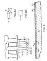
- FIG. 5 is a partly schematic view of the face of a representative semiconductor chip on which photodiodes, transistors, electrical leads, and the like, are fabricated for forming the electronic circuitry of an optical encoder.
- FIG. 5 is a partly schematic view of the face of a representative semiconductor chip on which photodiodes, transistors, electrical leads, and the like, are fabricated for forming the electronic circuitry of an optical encoder.
- Three areas of the chip are of interest in practice of this invention, with two of the areas being substantially similar to each other.
- the balance of the area on the representative chip is filled with conventional transistors and other components of the circuitry which form no part of this invention. Those portions of the chip are therefore indicated only with diagonal shading. It will be understood, however, that those portions of the chip occupied by transistors and the like are made in the same processing steps as the photodiodes employed in practice of this invention.
- the processes are conventional techniques for forming bipolar integrated circuits.
- a semiconductor chip comprises a substrate 18 (Fig. 6) of single crystal silicon or other semiconductor material.
- One face of the chip is modified by diffusion or implantation of impurities to affect the conduction properties of the silicon.
- a relatively high conductivity N doped buried layer 19 is formed in the silicon substrate for making electrical connections.
- a layer of lightly doped N-type epitaxial silicon 21 is deposited on the substrate. Selected areas of the epitaxial layer are doped with electron donors to form a highly doped N-type material in electrical contact with the buried layer.
- Dopants are then diffused into selected areas of the N-type material to form P-type material.
- N-type dopants are then diffused into such P-type regions for forming NPN transistors, or the like. Those transistors may be connected so that the N-type epitaxial layer forms the collector. A P-type area forms the base of the transistor and the final N-type material forms the emitter.
- the N-type epitaxial layer may be considered as a "collector” and the photodiodes 22 are formed of P-type "base” material. It will be apparent that polarities may be reversed and the epitaxial layer may be considered an emitter. Thus, the terms collector and base are used herein for purposes of exposition, rather than as terms of limitation.
- isolation barrier 23 Various areas on the semiconductor chip are isolated from each other by introducing dopants to form a high conductivity electrical isolation barrier 23.
- the isolation barrier is typically connected to electrical ground and isolates transistors from each other, and in this case, isolates photodiodes from areas occupied by transistors.
- the area within an electrical isolation barrier is sometimes referred to as a "tub".
- the isolation barrier is somewhat like two opposite diodes which provide electrical isolation. In CMOS technology, other electrical isolation barriers may be used.
- High conductivity electrical connection regions 24 may also be introduced for making electrical connection from the surface of the epitaxial layer to the buried layer.
- the surface is covered with silica or glass, and metal electrical leads are applied for making electrical connections to various areas of the chip (not shown in the drawings). It is conventional to apply a passivation layer over the entire chip, including the metal leads, for environmental protection when the chip is completed. If desired, an opaque layer (for example, of metal) may be deposited on the chip to provide a light mask for components on the chip. Such a mask may be applied over transistors in the circuit, for example, so that they are not photosensitive.
- bipolar devices on a semiconductor chip is, of course, quite conventional. It will also be understood that these manufacturing techniques are appropriate for the bipolar devices used in describing this invention, and for CMOS other technologies may be employed for fabricating suitable semiconductor chips.
- FIG. 5 illustrates a face of the semiconductor chip with a variety of somewhat superimposed features
- FIG. 7 is limited to a showing of the base layer for a representative chip made in accordance with practice of this invention.
- photodiodes 26, 27 there is an area or tub in which photodiodes 26, 27 are arrayed and isolated from the balance of the chip by an isolation barrier 28.
- a high conductivity region 29 implanted for making electrical contact to a buried layer (FIG. 6) which makes good electrical contact with the epitaxial collector layer.
- metal buses 31 on top of glass insulation (not shown) provide electrical contact for the four photodiodes in each of the several groups of photodiodes in the tub; there being eight groups in the illustrated embodiment.
- narrow "leads" 32 of base layer extend from each active photodiode 26 to a pad 33 to which electrical contact can be made by the respective metal bus.
- each of the inactive photodiodes is formed of the base layer so as to have the same width and electrical properties as the active photodiodes.
- the inactive photodiodes are shorted together by pads 34 of base layer, one of which is connected to the high conductivity area 29 leading to the buried layer and, hence, the collector. In other words, the inactive photodiodes are electrically shorted to themselves as indicated in FIG. 8B.
- the electrical connection of the active photodiodes is the same as in an encoder as described in the Leonard patent and in various commercial embodiments.
- Each of the similar photodiodes in the several groups are connected to the same metal bus so that their currents are additive.
- Each metal bus is in turn connected to an operational amplifier 36, the other lead of which is connected to the common collector for all of the photodiodes.
- the feedback for the operational amplifier employs a diode 37.
- the duty cycle where the outside photodiodes in a group are compared with the inside photodiodes of a group may not be symmetrical, thereby introducing an accuracy error. It has been found that the apparent source of this error is leakage current from outside the array of active photodiodes being different from leakage current from within the area occupied by active photodiodes.
- a substantial portion of the tub in which the array of photodiodes is placed is illuminated during operation of the encoder.
- a line 38 is shown in Fig. 5 around the area occupied by the photodiodes, and within the boundaries of the tub (as defined by the electrical isolation barrier 28). Areas outside the line 38 have an opaque coating of metal applied over the passivation layer, and areas inside the line remain exposed to illumination. This illumination generates hole and electron pairs, not only in the depletion region of the base-collector junction of the photodiodes, but also in the collector material.
- the holes have a relatively long lifetime and may diffuse laterally to be additive with current from the active photodiodes.
- the leakage current may arise from collector beneath the base layer of the photodiodes, from the small amount of collector layer exposed between adjacent photodiodes, and from portions of the tub exposed to light outside of the array of active and inactive photodiodes.
- a plurality of inactive photodiodes 27 are provided at each end of the array. With the leakage to the end and inner active photodiodes being equal, a source of duty cycle error is eliminated.
- the inactive photodiodes have a width, spacing and electrical properties substantially the same as the active photodiodes. A sufficient number of such inactive photodiodes are provided at each end of the array that the end photodiode is located in what is effectively a symmetrical array.
- the number of inactive photodiodes at each end of the array is a function of a number of factors. Generally speaking, it is desirable to have as many inactive photodiodes as possible so that the array of inactive photodiodes extends to the edge of the illuminated area in the tub.
- a factor in selecting the number of photodiodes to give the desired equality of leakage current for the end and inner photodiodes is the number of groups of photodiodes connected together by the metal buses for each channel of information. The larger the number of such groups, the less significant the current leakage problem is, since the effect on the end photodiode is essentially averaged with the other photodiodes with which is is connected.
- the size of the tub, or at least the illuminated area of the tub also has an effect. The larger the illuminated area, the more inactive photodiodes are desirable. As indicated above, it is preferable to essentially fill the tub or its illuminated area with the active and inactive photodiodes.
- the thickness and properties of the epitaxial layer forming the collector are also factors. A thicker layer permits the current carrying holes to diffuse further laterally before being swept up by the junction of an inactive or active photodiode. Electrical properties of significance include the lifetime of the holes (longer lifetime requiring more inactive photodiodes) and the ability to form electron-hole conduction pairs in the collector material. This latter is also a function of the frequency of light used in the encoder since the absorption coefficient of the semiconductor varies with frequency. The widths of the active and inactive photodiodes and the space between adjacent photodiodes also have an effect. Shallower photodiode junctions tend to produce greater leakage current as do wider strips of exposed collector between adjacent photodiodes.
- the decrease in leakage current carriers from the outside of the array of inactive photodiodes decreases exponentially. This tends to reduce the number of inactive photodiodes required to obtain substantial symmetry of boundary conditions for all of the active photodiodes, since only a fraction of the leakage current to each photodiode diffuses in turn to the following photodiode.
- the minimum number of inactive photodiodes is four. It is also desirable to have symmetry so that the number of inactive photodiodes at each end of the array of active photodiodes is the same.
- index apertures 41 are provided on the code wheel for indicating the absolute position of the code wheel.
- a plurality of such apertures are formed on a circumferentially extending track radially inwardly from the optical track 17, and another plurality of index apertures are provided radially outwardly from the optical track.
- a plurality of photodiodes 42 are provided in each of two tubs 43 radially inwardly and radially outwardly from the array of photodiodes 26 and 27.
- index photodiodes may also be sensitive to leakage current, which, if unbalanced between the inner and outer tracks of photodetectors, leads to duty cycle errors and uncertainty in the absolute position of the code wheel.
- the magnitude of such leakage currents is greatly reduced by providing a layer of base diffusion 44 which closely surrounds the index photodiodes and essentially fills all illuminated areas of the tub in which the index photodiodes are fabricated.
- a portion of the base layer filling the balance of the illuminated area extends laterally to make electrical contact with the isolation barrier. This causes a reverse bias on the photodiode junction between the inactive base layer 44 and the underlying collector. Because of the surrounding reverse biased junction, there is little leakage current from most of the tub to the index photodiodes and significant improvements in duty cycle are obtained.
- the number of photodiodes in each group may be six instead of four, or the number of groups may be increased or decreased as desired for a particular application to obtain the desired resolution, accuracy and contrast.
- the number of inactive photodiodes added to each end of the array of active photodiodes may be varied to obtain the desired degree of equality between the leakage current to the end photodiode in the array as compared with the leakage current to a photodiode remote from the end of the array.
- the photodiodes are not biased, it may be desirable in some embodiments to reverse bias the photodiodes to enhance light-current conversion efficiently and sensitivity.
Landscapes
- Physics & Mathematics (AREA)
- General Physics & Mathematics (AREA)
- Engineering & Computer Science (AREA)
- Theoretical Computer Science (AREA)
- Optical Transform (AREA)
- Light Receiving Elements (AREA)
Claims (8)
- Un encodeur optique qui comprend:
un réseau de photodiodes actives et inactives (26, 27) sur une microplaquette semi-conductrice;
un élément de codage (3) qui présente des zones agencées en alternance (13, 15) de manière à éclairer et à ne pas éclairer, en alternance, le réseau en réponse à un déplacement de l'élément de codage (3);
un moyen (36, 37) relié aux photodiodes actives (26) pour mesurer un courant produit par les photodiodes actives (26);
caractérisé en ce que les diodes inactives (27) sont agencées sous la forme d'une série de diodes inactives (27) disposées entre chaque diode active d'extrémité située sur l'extrémité du réseau et un bord d'une zone éclairée du réseau, la même série de photodiodes inactives (27) étant disposée à chaque extrémité du réseau, chacune desdites photodiodes inactives (27) présentant une largeur, un espacement et des propriétés électriques qui sont sensiblement les mêmes que pour chacune des photodiodes actives (26), un nombre suffisant desdites diodes inactives (27) étant agencé à chaque extrémité du réseau pour que le courant de fuite qui en provient vers la photodiode active d'extrémité (26) soit sensiblement le même que le courant de fuite qui va vers la diode active (26) d'extrémité à partir des autres photodiodes actives (26) du réseau, grâce à quoi le courant de fuite qui va vers chacune des photodiodes actives (26) du réseau est sensiblement le même de façon à minimiser une erreur de cycle opératoire. - Un encodeur optique selon la revendication 1, dans lequel les photodiodes inactives (27) sont électriquement mises en court-circuit sur elles-mêmes.
- Un encodeur optique selon la revendication 1, dans lequel ledit réseau de photodiodes (26, 27) est situé, sur la microplaquette semi-conductrice, à l'intérieur d'une zone séparée d'autres zones de la microplaquette par une barrière électriquement isolante, les photodiodes inactives (27) s'étendant sensiblement sur tout le trajet allant de la diode photoactive respective d'extrémité (26) jusqu'à la barrière isolante (23).
- Un encodeur optique selon la revendication 1, dans lequel chaque photodiode comprend un collecteur (21) de type N commun aux photodiodes et une base (22) de type P, la base (22) de type P de chaque photodiode active (26) étant reliée à une entrée d'un amplificateur opérationnel (36), le collecteur (21) étant relié à une autre entrée de l'amplificateur opérationnel (36); la base (22) de chaque photodiode inactive (27) étant reliée au collecteur (21).
- Un encodeur optique selon l'une quelconque des revendications précédentes, dans lequel l'élément de codage (3) est une roue de codage fonctionnant en tant qu'encodeur angulaire d'arbre.
- Un encodeur optique selon la revendication 5, dans lequel les photodiodes actives (26) sont agencées en vue d'une mesure de distance et au moins une photodiode (42) d'index est disposée sur une piste séparée du réseau desdites photodiodes actives (26), au moins une partie de la zone (43) de la microplaquette semi-conductrice qui entoure la photodiode d'index (42) étant elle aussi éclairée, en réponse à un déplacement de l'élément de codage (3), le reste principal de la zone éclairée non occupée par ladite photodiode (42) d'index étant une photodiode d'écran (43).
- Un encodeur optique selon la revendication 6, dans lequel le dopage de la photodiode d'écran (43) est le même que celui de ladite photodiode (42) d'index et dans lequel ladite photodiode d'écran (43) est électriquement reliée à la masse.
- Un encodeur optique selon la revendication 6, incluant en outre un moyen de polarisation de la jonction de photodiode de zone d'écran, soit selon une polarisation nulle, soit selon une polarisation inverse.
Applications Claiming Priority (2)
| Application Number | Priority Date | Filing Date | Title |
|---|---|---|---|
| US07/290,542 US4904861A (en) | 1988-12-27 | 1988-12-27 | Optical encoder using sufficient inactive photodetectors to make leakage current equal throughout |
| US290542 | 1988-12-27 |
Publications (3)
| Publication Number | Publication Date |
|---|---|
| EP0376538A2 EP0376538A2 (fr) | 1990-07-04 |
| EP0376538A3 EP0376538A3 (fr) | 1992-10-21 |
| EP0376538B1 true EP0376538B1 (fr) | 1995-08-09 |
Family
ID=23116481
Family Applications (1)
| Application Number | Title | Priority Date | Filing Date |
|---|---|---|---|
| EP89312949A Expired - Lifetime EP0376538B1 (fr) | 1988-12-27 | 1989-12-12 | Codeur optique à photodétecteurs inactifs |
Country Status (4)
| Country | Link |
|---|---|
| US (1) | US4904861A (fr) |
| EP (1) | EP0376538B1 (fr) |
| JP (1) | JP2749408B2 (fr) |
| DE (1) | DE68923780T2 (fr) |
Families Citing this family (73)
| Publication number | Priority date | Publication date | Assignee | Title |
|---|---|---|---|---|
| US5640007A (en) * | 1995-06-21 | 1997-06-17 | Limitorque Corporation | Optical encoder comprising a plurality of encoder wheels |
| US5844814A (en) * | 1996-09-27 | 1998-12-01 | International Business Machines Corporation | Optical position sensing device and method for sub-micron measurement |
| US5977571A (en) * | 1998-02-26 | 1999-11-02 | Lucent Technologies, Inc. | Low loss connecting arrangement for photodiodes |
| US6133615A (en) * | 1998-04-13 | 2000-10-17 | Wisconsin Alumni Research Foundation | Photodiode arrays having minimized cross-talk between diodes |
| US6355927B1 (en) * | 1999-08-20 | 2002-03-12 | Agilent Technologies, Inc. | Interpolation methods and circuits for increasing the resolution of optical encoders |
| US6563108B1 (en) | 1999-10-25 | 2003-05-13 | Quantum Devices, Inc. | System for tracking angular and linear motion |
| US6590201B2 (en) | 1999-12-22 | 2003-07-08 | Rohm Co., Ltd. | Optical encoder incorporating linear light controlling member |
| JP2004309387A (ja) * | 2003-04-09 | 2004-11-04 | Toshiba Corp | 光学式エンコーダ |
| US8686529B2 (en) | 2010-01-19 | 2014-04-01 | Osi Optoelectronics, Inc. | Wavelength sensitive sensor photodiodes |
| US7880258B2 (en) * | 2003-05-05 | 2011-02-01 | Udt Sensors, Inc. | Thin wafer detectors with improved radiation damage and crosstalk characteristics |
| US8164151B2 (en) * | 2007-05-07 | 2012-04-24 | Osi Optoelectronics, Inc. | Thin active layer fishbone photodiode and method of manufacturing the same |
| US8120023B2 (en) * | 2006-06-05 | 2012-02-21 | Udt Sensors, Inc. | Low crosstalk, front-side illuminated, back-side contact photodiode array |
| US7279731B1 (en) | 2006-05-15 | 2007-10-09 | Udt Sensors, Inc. | Edge illuminated photodiodes |
| US7655999B2 (en) | 2006-09-15 | 2010-02-02 | Udt Sensors, Inc. | High density photodiodes |
| US7256470B2 (en) * | 2005-03-16 | 2007-08-14 | Udt Sensors, Inc. | Photodiode with controlled current leakage |
| US7709921B2 (en) | 2008-08-27 | 2010-05-04 | Udt Sensors, Inc. | Photodiode and photodiode array with improved performance characteristics |
| US8035183B2 (en) * | 2003-05-05 | 2011-10-11 | Udt Sensors, Inc. | Photodiodes with PN junction on both front and back sides |
| US7656001B2 (en) * | 2006-11-01 | 2010-02-02 | Udt Sensors, Inc. | Front-side illuminated, back-side contact double-sided PN-junction photodiode arrays |
| US8519503B2 (en) * | 2006-06-05 | 2013-08-27 | Osi Optoelectronics, Inc. | High speed backside illuminated, front side contact photodiode array |
| US7057254B2 (en) * | 2003-05-05 | 2006-06-06 | Udt Sensors, Inc. | Front illuminated back side contact thin wafer detectors |
| US7576369B2 (en) * | 2005-10-25 | 2009-08-18 | Udt Sensors, Inc. | Deep diffused thin photodiodes |
| US7242069B2 (en) * | 2003-05-05 | 2007-07-10 | Udt Sensors, Inc. | Thin wafer detectors with improved radiation damage and crosstalk characteristics |
| JP2005017116A (ja) * | 2003-06-26 | 2005-01-20 | Sharp Corp | 光学式エンコーダ用受光素子 |
| US6816091B1 (en) * | 2003-12-18 | 2004-11-09 | Agilent Technologies, Inc. | Interpolator |
| US7955357B2 (en) | 2004-07-02 | 2011-06-07 | Ellipse Technologies, Inc. | Expandable rod system to treat scoliosis and method of using the same |
| JP2006138775A (ja) * | 2004-11-12 | 2006-06-01 | Toshiba Corp | 光学式エンコーダ用受光素子及び光学式エンコーダ |
| US7862502B2 (en) | 2006-10-20 | 2011-01-04 | Ellipse Technologies, Inc. | Method and apparatus for adjusting a gastrointestinal restriction device |
| US9178092B2 (en) | 2006-11-01 | 2015-11-03 | Osi Optoelectronics, Inc. | Front-side illuminated, back-side contact double-sided PN-junction photodiode arrays |
| US20090112263A1 (en) | 2007-10-30 | 2009-04-30 | Scott Pool | Skeletal manipulation system |
| US20100053802A1 (en) * | 2008-08-27 | 2010-03-04 | Masaki Yamashita | Low Power Disk-Drive Motor Driver |
| US11202707B2 (en) | 2008-03-25 | 2021-12-21 | Nuvasive Specialized Orthopedics, Inc. | Adjustable implant system |
| GB2476019B (en) * | 2008-09-15 | 2013-03-13 | Osi Optoelectronics Inc | Thin active layer fishbone photodiode with a shallow N+ layer and method of manufacturing the same |
| US11241257B2 (en) | 2008-10-13 | 2022-02-08 | Nuvasive Specialized Orthopedics, Inc. | Spinal distraction system |
| US8382756B2 (en) | 2008-11-10 | 2013-02-26 | Ellipse Technologies, Inc. | External adjustment device for distraction device |
| US8197490B2 (en) | 2009-02-23 | 2012-06-12 | Ellipse Technologies, Inc. | Non-invasive adjustable distraction system |
| US9622792B2 (en) | 2009-04-29 | 2017-04-18 | Nuvasive Specialized Orthopedics, Inc. | Interspinous process device and method |
| US8399909B2 (en) * | 2009-05-12 | 2013-03-19 | Osi Optoelectronics, Inc. | Tetra-lateral position sensing detector |
| EP2473116B1 (fr) | 2009-09-04 | 2019-12-04 | NuVasive Specialized Orthopedics, Inc. | Dispositif de croissance osseuse |
| US9248043B2 (en) | 2010-06-30 | 2016-02-02 | Ellipse Technologies, Inc. | External adjustment device for distraction device |
| WO2012021378A2 (fr) | 2010-08-09 | 2012-02-16 | Ellipse Technologies, Inc. | Élément de maintenance dans un implant magnétique |
| WO2012112396A2 (fr) | 2011-02-14 | 2012-08-23 | Ellipse Technologies, Inc. | Dispositif et méthode de traitement d'os fracturés |
| US10743794B2 (en) | 2011-10-04 | 2020-08-18 | Nuvasive Specialized Orthopedics, Inc. | Devices and methods for non-invasive implant length sensing |
| US10016220B2 (en) | 2011-11-01 | 2018-07-10 | Nuvasive Specialized Orthopedics, Inc. | Adjustable magnetic devices and methods of using same |
| US20130338714A1 (en) | 2012-06-15 | 2013-12-19 | Arvin Chang | Magnetic implants with improved anatomical compatibility |
| US9044281B2 (en) | 2012-10-18 | 2015-06-02 | Ellipse Technologies, Inc. | Intramedullary implants for replacing lost bone |
| CN104902854B (zh) | 2012-10-29 | 2017-10-03 | 诺威适骨科专科公司 | 用于治疗膝盖关节炎的可调节装置 |
| US8912615B2 (en) | 2013-01-24 | 2014-12-16 | Osi Optoelectronics, Inc. | Shallow junction photodiode for detecting short wavelength light |
| US9179938B2 (en) | 2013-03-08 | 2015-11-10 | Ellipse Technologies, Inc. | Distraction devices and method of assembling the same |
| US10226242B2 (en) | 2013-07-31 | 2019-03-12 | Nuvasive Specialized Orthopedics, Inc. | Noninvasively adjustable suture anchors |
| US9801734B1 (en) | 2013-08-09 | 2017-10-31 | Nuvasive, Inc. | Lordotic expandable interbody implant |
| US10751094B2 (en) | 2013-10-10 | 2020-08-25 | Nuvasive Specialized Orthopedics, Inc. | Adjustable spinal implant |
| US9857205B2 (en) | 2013-11-06 | 2018-01-02 | Quantum Devices, Inc. | Encoder system with a desired radial alignment and axial gap |
| CN111345867A (zh) | 2014-04-28 | 2020-06-30 | 诺威适骨科专科公司 | 遥控装置 |
| KR102588501B1 (ko) | 2014-10-23 | 2023-10-11 | 누베이시브 스페셜라이즈드 오소페딕스, 인크. | 원격으로 조정 가능한 상호작용적 뼈 재성형 임플란트 |
| EP4005515B1 (fr) | 2014-12-26 | 2024-07-24 | NuVasive Specialized Orthopedics, Inc. | Systèmes de distraction |
| US10238427B2 (en) | 2015-02-19 | 2019-03-26 | Nuvasive Specialized Orthopedics, Inc. | Systems and methods for vertebral adjustment |
| WO2017066774A1 (fr) | 2015-10-16 | 2017-04-20 | Nuvasive Specialized Orthopedics, Inc. | Dispositifs ajustables pour traiter l'arthrite du genou |
| JP6953409B2 (ja) | 2015-12-10 | 2021-10-27 | ニューベイシブ スペシャライズド オーソペディックス,インコーポレイテッド | 伸延デバイス用の外部調整デバイス |
| DK3407812T3 (da) | 2016-01-28 | 2020-09-21 | Nuvasive Specialized Orthopedics Inc | System til knogletransport |
| WO2017139548A1 (fr) | 2016-02-10 | 2017-08-17 | Nuvasive Specialized Orthopedics, Inc. | Systèmes et procédés de commande de variables chirurgicales multiples |
| EP3922039A1 (fr) | 2019-02-07 | 2021-12-15 | NuVasive Specialized Orthopedics, Inc. | Communication ultrasonore dans des dispositifs médicaux |
| US11589901B2 (en) | 2019-02-08 | 2023-02-28 | Nuvasive Specialized Orthopedics, Inc. | External adjustment device |
| WO2021045946A1 (fr) | 2019-09-03 | 2021-03-11 | Nuvasive Specialized Orthopedics, Inc. | Rapport acoustique pour implants dynamiques |
| US12605192B2 (en) | 2020-07-15 | 2026-04-21 | Globus Medical, Inc. | Ultrasonic communication in adjustable implants |
| US12213708B2 (en) | 2020-09-08 | 2025-02-04 | Nuvasive Specialized Orthopedics, Inc. | Remote control module for adjustable implants |
| US11806054B2 (en) | 2021-02-23 | 2023-11-07 | Nuvasive Specialized Orthopedics, Inc. | Adjustable implant, system and methods |
| US11737787B1 (en) | 2021-05-27 | 2023-08-29 | Nuvasive, Inc. | Bone elongating devices and methods of use |
| AU2022325024A1 (en) | 2021-08-03 | 2024-02-22 | Nuvasive Specialized Orthopedics, Inc. | Adjustable implant |
| US12551240B2 (en) | 2022-06-13 | 2026-02-17 | Nuvasive Inc. | Distraction loss magnet on-off mechanism |
| US12458417B2 (en) | 2022-08-15 | 2025-11-04 | Nuvasive Specialized Orthopedics Inc. | Intermedullary lengthening implant with integrated load sensor |
| US12508058B2 (en) | 2022-10-07 | 2025-12-30 | Nuvasive Specialized Orthopedics, Inc. | Adjustable tether implant |
| US12558133B2 (en) | 2023-04-25 | 2026-02-24 | Nuvasive, Inc. | Flat plate mechanisms for bone lengthening |
| US12533164B2 (en) | 2023-05-03 | 2026-01-27 | Nuvasive Specialized Orthopedics, Inc. | Adjustable implant |
Family Cites Families (11)
| Publication number | Priority date | Publication date | Assignee | Title |
|---|---|---|---|---|
| US3757128A (en) * | 1972-03-20 | 1973-09-04 | Ibm | Multiphase tachometer |
| US4675549A (en) * | 1978-02-06 | 1987-06-23 | Fairchild Camera And Instrument Corporation | Black and white reference and end-of-scan indicator for charge coupled devices |
| JPS54130828A (en) * | 1978-03-31 | 1979-10-11 | Canon Inc | Photo sensor array device and image scanner using it |
| US4259570A (en) * | 1978-11-27 | 1981-03-31 | Hewlett-Packard Company | Optical comparator |
| US4266125A (en) * | 1978-12-21 | 1981-05-05 | Hewlett-Packard Company | Optical shaft angle encoder |
| US4341956A (en) * | 1979-09-24 | 1982-07-27 | Pfizer, Inc. | Apparatus and method for compensating the dark current photoelectric transducers |
| US4451731A (en) * | 1981-08-10 | 1984-05-29 | Hewlett-Packard Company | Apparatus and method for modulating light to generate an index pulse |
| JPS59154880A (ja) * | 1983-02-24 | 1984-09-03 | Asahi Optical Co Ltd | 光電出力のダ−ク電流補償回路 |
| US4661696A (en) * | 1985-06-04 | 1987-04-28 | Plus Development Corporation | Optical encoder which use a rectangular photodetector array |
| US4691101A (en) * | 1985-06-19 | 1987-09-01 | Hewlett-Packard Company | Optical positional encoder comprising immediately adjacent detectors |
| JPS6226970A (ja) * | 1985-07-26 | 1987-02-04 | Nec Corp | 電荷検出回路 |
-
1988
- 1988-12-27 US US07/290,542 patent/US4904861A/en not_active Expired - Lifetime
-
1989
- 1989-12-12 EP EP89312949A patent/EP0376538B1/fr not_active Expired - Lifetime
- 1989-12-12 DE DE68923780T patent/DE68923780T2/de not_active Expired - Lifetime
- 1989-12-22 JP JP1334585A patent/JP2749408B2/ja not_active Expired - Lifetime
Also Published As
| Publication number | Publication date |
|---|---|
| DE68923780T2 (de) | 1995-12-21 |
| DE68923780D1 (de) | 1995-09-14 |
| EP0376538A2 (fr) | 1990-07-04 |
| US4904861A (en) | 1990-02-27 |
| JP2749408B2 (ja) | 1998-05-13 |
| JPH02221812A (ja) | 1990-09-04 |
| EP0376538A3 (fr) | 1992-10-21 |
Similar Documents
| Publication | Publication Date | Title |
|---|---|---|
| US4904861A (en) | Optical encoder using sufficient inactive photodetectors to make leakage current equal throughout | |
| US4998013A (en) | Optical encoder with inactive photodetectors | |
| US5576537A (en) | Photoelectric position measuring system using gratings having specified dimensions to suppress harmonics | |
| US6875974B2 (en) | Device for detecting the angle of incidence of radiation on a radiation incidence surface | |
| US7098446B2 (en) | Photoelectric encoder | |
| US20090236507A1 (en) | Shaft-mounted detector for optical encoder | |
| JPH0832100A (ja) | 受光素子 | |
| US6906311B2 (en) | Photoelectric encoder | |
| JP4425220B2 (ja) | アブソリュートエンコーダ | |
| US20010011699A1 (en) | Displacement measuring apparatus | |
| GB2094974A (en) | Photoelectric encoder device | |
| JP2010048833A (ja) | 光電式エンコーダ | |
| US6956200B2 (en) | Phase-shift photoelectric encoder | |
| US4766307A (en) | Semiconductive radial photodetector and apparatus comprising such a detector | |
| Schmidt et al. | Position-sensitive photodetectors made with standard silicon-planar technology | |
| KR100569506B1 (ko) | 반도체 위치 검출기 | |
| JP2610624B2 (ja) | 光学式変位検出器 | |
| US7095011B2 (en) | Photoelectric encoder for precise measurements | |
| JP4372566B2 (ja) | 光電式エンコーダ | |
| JP3315938B2 (ja) | 半導体暗像位置検出素子 | |
| JP3946561B2 (ja) | 光電式エンコーダの原点検出装置 | |
| JP4444715B2 (ja) | 光学式変位測定装置 | |
| US20070241268A1 (en) | Encoder module adapted for a plurality of different resolutions | |
| US4827122A (en) | Rotation angle detector | |
| RU50048U1 (ru) | Многоэлементный кодовый фотоприемник |
Legal Events
| Date | Code | Title | Description |
|---|---|---|---|
| PUAI | Public reference made under article 153(3) epc to a published international application that has entered the european phase |
Free format text: ORIGINAL CODE: 0009012 |
|
| AK | Designated contracting states |
Kind code of ref document: A2 Designated state(s): DE FR GB |
|
| PUAL | Search report despatched |
Free format text: ORIGINAL CODE: 0009013 |
|
| AK | Designated contracting states |
Kind code of ref document: A3 Designated state(s): DE FR GB |
|
| 17P | Request for examination filed |
Effective date: 19930330 |
|
| 17Q | First examination report despatched |
Effective date: 19940712 |
|
| GRAA | (expected) grant |
Free format text: ORIGINAL CODE: 0009210 |
|
| AK | Designated contracting states |
Kind code of ref document: B1 Designated state(s): DE FR GB |
|
| REF | Corresponds to: |
Ref document number: 68923780 Country of ref document: DE Date of ref document: 19950914 |
|
| ET | Fr: translation filed | ||
| PLBE | No opposition filed within time limit |
Free format text: ORIGINAL CODE: 0009261 |
|
| STAA | Information on the status of an ep patent application or granted ep patent |
Free format text: STATUS: NO OPPOSITION FILED WITHIN TIME LIMIT |
|
| 26N | No opposition filed | ||
| PGFP | Annual fee paid to national office [announced via postgrant information from national office to epo] |
Ref country code: FR Payment date: 19961115 Year of fee payment: 8 |
|
| PGFP | Annual fee paid to national office [announced via postgrant information from national office to epo] |
Ref country code: GB Payment date: 19961128 Year of fee payment: 8 |
|
| PG25 | Lapsed in a contracting state [announced via postgrant information from national office to epo] |
Ref country code: GB Free format text: LAPSE BECAUSE OF NON-PAYMENT OF DUE FEES Effective date: 19971212 |
|
| PG25 | Lapsed in a contracting state [announced via postgrant information from national office to epo] |
Ref country code: FR Free format text: THE PATENT HAS BEEN ANNULLED BY A DECISION OF A NATIONAL AUTHORITY Effective date: 19971231 |
|
| GBPC | Gb: european patent ceased through non-payment of renewal fee |
Effective date: 19971212 |
|
| REG | Reference to a national code |
Ref country code: FR Ref legal event code: ST |
|
| PGFP | Annual fee paid to national office [announced via postgrant information from national office to epo] |
Ref country code: DE Payment date: 20081205 Year of fee payment: 20 |