EP0376722B1 - Herstellungsprozess für bipolare Sinkerstruktur - Google Patents
Herstellungsprozess für bipolare Sinkerstruktur Download PDFInfo
- Publication number
- EP0376722B1 EP0376722B1 EP89313647A EP89313647A EP0376722B1 EP 0376722 B1 EP0376722 B1 EP 0376722B1 EP 89313647 A EP89313647 A EP 89313647A EP 89313647 A EP89313647 A EP 89313647A EP 0376722 B1 EP0376722 B1 EP 0376722B1
- Authority
- EP
- European Patent Office
- Prior art keywords
- sinker
- layer
- buried layer
- trench
- substrate
- Prior art date
- Legal status (The legal status is an assumption and is not a legal conclusion. Google has not performed a legal analysis and makes no representation as to the accuracy of the status listed.)
- Expired - Lifetime
Links
- 238000000034 method Methods 0.000 title claims description 25
- 239000000758 substrate Substances 0.000 claims description 21
- 239000000463 material Substances 0.000 claims description 12
- 239000002019 doping agent Substances 0.000 claims description 5
- 238000005530 etching Methods 0.000 claims description 4
- 230000000149 penetrating effect Effects 0.000 claims 1
- 238000009792 diffusion process Methods 0.000 description 9
- 230000000873 masking effect Effects 0.000 description 8
- 230000015572 biosynthetic process Effects 0.000 description 7
- 238000013459 approach Methods 0.000 description 3
- 238000002955 isolation Methods 0.000 description 3
- 238000010438 heat treatment Methods 0.000 description 2
- 150000004767 nitrides Chemical class 0.000 description 2
- 229910021420 polycrystalline silicon Inorganic materials 0.000 description 2
- 229920005591 polysilicon Polymers 0.000 description 2
- 238000012545 processing Methods 0.000 description 2
- 238000012552 review Methods 0.000 description 2
- 238000013461 design Methods 0.000 description 1
- 230000009977 dual effect Effects 0.000 description 1
- 239000012535 impurity Substances 0.000 description 1
- 230000010354 integration Effects 0.000 description 1
- 230000003071 parasitic effect Effects 0.000 description 1
- 238000001020 plasma etching Methods 0.000 description 1
- 239000004065 semiconductor Substances 0.000 description 1
- 229910021332 silicide Inorganic materials 0.000 description 1
- FVBUAEGBCNSCDD-UHFFFAOYSA-N silicide(4-) Chemical compound [Si-4] FVBUAEGBCNSCDD-UHFFFAOYSA-N 0.000 description 1
- 125000006850 spacer group Chemical group 0.000 description 1
Images


Classifications
-
- H—ELECTRICITY
- H10—SEMICONDUCTOR DEVICES; ELECTRIC SOLID-STATE DEVICES NOT OTHERWISE PROVIDED FOR
- H10D—INORGANIC ELECTRIC SEMICONDUCTOR DEVICES
- H10D62/00—Semiconductor bodies, or regions thereof, of devices having potential barriers
- H10D62/10—Shapes, relative sizes or dispositions of the regions of the semiconductor bodies; Shapes of the semiconductor bodies
- H10D62/13—Semiconductor regions connected to electrodes carrying current to be rectified, amplified or switched, e.g. source or drain regions
- H10D62/137—Collector regions of BJTs
Definitions
- the present invention is related to high performance bipolar devices and more particularly a low resistance connection from the wafer surface to the buried layer, often referred to as a "sinker" in a bipolar device structure and a process for forming that sinker.
- the sinker and the process for forming it disclosed in this application are especially useful in the formation of devices of the type disclosed in EP-A-0 324 580 assigned to the assignee of this invention. Details of a complete bipolar process in which this sinker and related process may be efficiently incorporated may be found in EP-A-0 337 720, also assigned to the assignee of this invention.
- the present trend in semiconductor technology is toward large scale of integration of devices with very high speed and low power consumption performance.
- the parameters that are essential to such high performance bipolar transistors include the presence of low parasitic capacitances as realized by shallow vertical junctions and small horizontal geometries. In other words it is necessary to make the devices in the integrated circuit as small as possible in both the horizontal and vertical directions.
- bipolar devices incorporate a sinker, that is a heavily doped region extending from the surface of the substrate through the top epitaxial layer down to the buried layer to provide a low resistivity connection from the N- collector of the epi-region to the low resistance N+ buried layer.
- the buried layer will thereafter provide the low resistance lateral contact which extends under the bipolar device.
- the purpose in any bipolar device is to minimize the collector resistance.
- a cell design was disclosed which helped solve this problem by reducing the distance from emitter to collector to lower the lateral spacing and thereby the collector resistance.
- FIG 1 The standard approach in the prior art is as shown in FIG 1 wherein the collector and sinker are located in a region 2 separated by an oxide isolation 4 from the emitter and base generally indicated at 6 of the bipolar device.
- the sinker in such a structure is formed by cutting a hole in the oxide, doing a masking step and diffusing the N+ sinker 7 from the surface. The result is a sidewise diffusion as well as a deep diffusion, resulting in the devotion of considerable area (as illustrated in FIG 1) to the collector and associated sinker.
- the complete bipolar device is typically defined in a tub 8 edged by trenches 10, 12 which tub extends down through the epitaxial layer 14 and buried layer 16 to the substrate region 18.
- trenches 10, 12 which tub extends down through the epitaxial layer 14 and buried layer 16 to the substrate region 18.
- EP-A-0112489 discloses providing a substrate comprising a base layer of P-type material, a buried layer of N + -type material extending over the base layer, and an epitaxial layer of N-type material extending over the buried layer.
- a mask is provided on the substrate having an opening to define the location of a trench. Reactive ion etching is then performed through the opening to form the trench through the epitaxial layer and reaching the buried layer.
- An impurity diffusion is then performed to form an N + -type layer in the side walls and bottom surface of the trench. Then the bottom surface of the trench is further etched to extend through the buried layer to expose the P-type base layer.
- the N + -type layer diffused in the side walls of the trench connect the buried layer with an n + type contact region on the top surface of the substrate, while the trench forms an isolation trench.
- US-A-4140558 discloses a similar process.
- Examples of the invention incorporate a sinker in a bipolar device without a significant increase in process complexity.
- the invention provides a method of forming a sinker self-aligned with an isolating trench used to define a tub in a substrate of at least one bipolar device, said substrate comprising a base layer of P-type material, a buried layer of N-type material extending over the surface of said base layer, and an epitaxial layer of N-type material extending over the surface of said buried layer, said method comprising the steps of:
- the device is formed in the tub preferably with the collector adjacent the trench and thereby aligned with the sinker.
- the collector or dual collectors of the bipolar device are preferably placed immediately adjacent the isolating trench. Therefore, the collector may be only a shallow junction, but is inherently immediately self-aligned with the sinker, providing a low-resistance contact, aligned with the collector, from the collector through the sinker to the buried layer to minimize the collector resistance of the device.
- the process begins with a substrate 18 on which a uniform, unmasked buried layer of an opposite polarity type to the substrate is formed.
- the substrate will be P-type material, and the buried layer an N+ type material.
- a uniform N- epitaxial layer 14 is then formed over the buried layer.
- an oxide layer 20 is grown over the surface of the epitaxial layer.
- a layer of nitride (not shown in FIG 2A) may be placed under the oxide to form the necessary stack so that selective etching of the nitride layers below this oxide to define the active device areas.
- a masking step is then used to define an opening or hole 22 where the trench 10, 12 will be established.
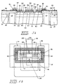
- the hole 22 is first used as a masked opening for a diffusion to create a diffused region 30 which extends at least through the epitaxial layer 14 into the buried layer 16. Since the diffusion will be both vertical and lateral, although the dopant is introduced through the opening which will be used to define the trench, a portion of the dopant will extend and diffuse sideways beneath the oxide, extending laterally beyond the region where the trench or its slot 10 will be cut. Thereafter, in a single step, the trench 10 is cut through the layers 14 and 16 into the substrate 18. Because of the sideways diffusion discussed above, a sinker 26 inherently self-aligned with the isolating trench 10 has been created without additional masking.
- the formation of the sinker 26 fits in with the formation of the bipolar device as formed in accordance with the referenced application without additional masking steps, and with the collectors of the finished bipolar device being inherently and directly aligned with the sinker to provide a low resistance contact from collector to buried layer.
- the next masking step is to define the field oxide 46 which will surround the bipolar device and isolate it from adjoining devices, as well as providing a support layer for connections to be formed.
- the active base region 50 is formed and the N+ polysilicon layer (which will form, contacts 52, 54, 56) is deposited.
- a thin silicide layer 57 is formed and topped with an oxide 61.
- the polysilicon emitter and collector contacts 50, 52, 54, 56 are then aligned and masked relative to the base 50.
- the spacers 60 are defined adjacent the emitter and collector.
- the subsequent heating steps will define the active collector 63 and emitter 64 by diffusion of the dopant from the poly 52, 54, 56 into the epitaxial layer 18. As can be seen, this diffusion step immediately brings the collector 63 into contact with the sinker 26 to provide the desired low resistance contact for the collector to the buried layer 16.
- the upper layer of P-doped poly 68 is then laid down and heating will define the extrinsic base regions 69 and 70, creating contact between the upper poly material and active intrinsic base 50 to complete formation of the device.
- the above processes provide a self-aligned, horizontally limited, heavily doped sinker which provides an effective collector to buried layer low resistance contact.
- the sinker can be very accurately defined, and either placed or excluded as is necessary with additional masking to meet the requirements of different device structures, or if one wishes to limit sinker only to collector contact areas.
- the sinker region 26 as seen in a top plan view is typically an annulus along the wall of the isolation slot 10 which surrounds the bipolar device shown in FIG 3A. However, the region 26 can be masked to contact only a portion of the collector contact 63.
- This sinker can be placed around the entire perimeter of all N- epi tubs without the use of additional masking steps (maskless sinker process). If the maskless sinker process is chosen, proper care must be taken in layout rule definition to allow sufficient space 103 for field oxide 46 to overlap the active area adjacent to base contacts 69 and 70, and emitters 64.
Landscapes
- Bipolar Transistors (AREA)
- Element Separation (AREA)
- Electrodes Of Semiconductors (AREA)
Claims (6)
- Verfahren zur Herstellung einer mit einem isolierenden Graben (10), der zum Definieren einer Wanne in einem Substrat mindestens einer bipolaren Vorrichtung verwendet wird, selbstjustierten Platine (26), wobei das Substrat eine Grundschicht (18) p-Typ-Materials, eine vergrabene Schicht (16) n-Typ-Materials, die sich über die Oberfläche der Grundschicht erstreckt, und eine Epitaxieschicht (14) n-Typ-Materials, die sich über die Oberfläche der versteckten Schicht erstreckt, aufweist, wobei das Verfahren folgende Schritte aufweist:(a) Definieren einer Maske auf dem Substrat mit einer Öffnung, die mindestens teilweise über einem Bereich liegt, unter dem die Platine (26) und der isolierende Graben (10) gebildet werden sollen,(b) Definieren, durch die Maskenöffnung hindurch, eines n-Typ-dotierten Bereichs (26, 30), der sich von der Substratoberfläche durch die Epitaxieschicht (14) und in die vergrabene Schicht (16) hinein, aber nicht durch sie hindurch, erstreckt, wobei der dotierte Bereich sich weiter lateral in der Epitaxieschicht (14) er- streckt als in der unterliegenden vergrabenen Schicht (16), und(c) Ätzen des Substrats durch die Maskenöffnung, um den isolierenden Graben (10), der sich durch die Epitaxieschicht (14) und durch die vergrabene Schicht (16) hindurch und in die Grundschicht (18) hinein, aber nicht durch diese hindurch, erstreckt, zu bilden,
wobei der bei Schritt (b) definierte n-dotierte Bereich eine Platine (26) bildet, die mit dem isolierenden Graben selbstjustiert ist, und wobei der isolierende Graben einen äußeren Begrenzungsrand der Wanne bildet. - Verfahren nach Anspruch 1, wobei der Schritt (b) beinhaltet: Einführen, durch die Maskenöffnung, eines Dotanden, der mindestens in einen darunterliegenden Bereich der vergrabenen Schicht eindringt.
- Verfahren nach einem der Ansprüche 1 und 2, wobei der Schritt (b) folgenden Schritt beinhaltet: Bewirken, daß der Dotand lateral über einen Bereich hinausdringt, der nachfolgend durch den in Schritt (c) gebildeten isolierenden Graben durchschnitten wird.
- Verfahren nach einem der Ansprüche 1 bis 3, das folgenden Schritt beinhaltet: Definieren einer bipolaren Vorrichtung in der Wanne mit einem Kollektorkontaktbereich (54, 56), der zu dem Graben benachbart ausgebildet ist und die Platine zumindestens teilweise bedeckt, wobei die Platine den Kollektorkontaktbereich elektrisch mit der vergrabenen Schicht verbindet.
- Verfahren nach Anspruch 4, wobei die bipolare Vorrichtung einen ersten und einen zweiten Kollektorkontaktbereich (54, 56) beinhaltet, von denen jeder zu dem Graben benachbart ausgebildet ist und die Platine zumindestens teilweise bedeckt.
- Verfahren nach einem der Ansprüche 1 bis 5, wobei Schritt (c) folgendes beinhaltet: Ätzen des Substrats, um mindestens einen isolierenden Graben zu bilden, der sich durch die Epitaxieschicht, durch die vergrabene Schicht und in die Grundschicht hinein, aber nicht durch diese hindurch, erstreckt, wobei der mindestens eine isolierende Graben anders als durch die Maskenöffnung gebildet wird.
Applications Claiming Priority (2)
| Application Number | Priority Date | Filing Date | Title |
|---|---|---|---|
| US291185 | 1988-12-28 | ||
| US07/291,185 US5001538A (en) | 1988-12-28 | 1988-12-28 | Bipolar sinker structure and process for forming same |
Publications (3)
| Publication Number | Publication Date |
|---|---|
| EP0376722A2 EP0376722A2 (de) | 1990-07-04 |
| EP0376722A3 EP0376722A3 (de) | 1990-10-17 |
| EP0376722B1 true EP0376722B1 (de) | 2000-11-29 |
Family
ID=23119247
Family Applications (1)
| Application Number | Title | Priority Date | Filing Date |
|---|---|---|---|
| EP89313647A Expired - Lifetime EP0376722B1 (de) | 1988-12-28 | 1989-12-28 | Herstellungsprozess für bipolare Sinkerstruktur |
Country Status (4)
| Country | Link |
|---|---|
| US (1) | US5001538A (de) |
| EP (1) | EP0376722B1 (de) |
| JP (1) | JPH02263442A (de) |
| DE (1) | DE68929268T2 (de) |
Families Citing this family (5)
| Publication number | Priority date | Publication date | Assignee | Title |
|---|---|---|---|---|
| US5614750A (en) * | 1995-06-29 | 1997-03-25 | Northern Telecom Limited | Buried layer contact for an integrated circuit structure |
| US6703679B1 (en) | 1999-08-31 | 2004-03-09 | Analog Devices, Imi, Inc. | Low-resistivity microelectromechanical structures with co-fabricated integrated circuit |
| US6818958B2 (en) * | 2001-04-13 | 2004-11-16 | International Rectifier Corporation | Semiconductor device and process for its manufacture to increase threshold voltage stability |
| US6699765B1 (en) * | 2002-08-29 | 2004-03-02 | Micrel, Inc. | Method of fabricating a bipolar transistor using selective epitaxially grown SiGe base layer |
| EP1696485A1 (de) * | 2005-02-24 | 2006-08-30 | STMicroelectronics S.r.l. | Verfahren zur Herstellung von Halbleiterbauelementen in einem SOI-Substrat mit Justiermarken |
Family Cites Families (19)
| Publication number | Priority date | Publication date | Assignee | Title |
|---|---|---|---|---|
| US4047220A (en) * | 1975-12-24 | 1977-09-06 | General Electric Company | Bipolar transistor structure having low saturation resistance |
| US4140558A (en) * | 1978-03-02 | 1979-02-20 | Bell Telephone Laboratories, Incorporated | Isolation of integrated circuits utilizing selective etching and diffusion |
| US4691219A (en) * | 1980-07-08 | 1987-09-01 | International Business Machines Corporation | Self-aligned polysilicon base contact structure |
| EP0068070A1 (de) * | 1981-07-01 | 1983-01-05 | Rockwell International Corporation | Komplementare NPN- und PNP-Lateraltransistoren, die zur minimalen Beeinflussung durch mit Substratoxyd gefüllte Rillen vom Substrat getrennt sind, und Verfahren zu ihrer Herstellung |
| JPS5992548A (ja) * | 1982-11-18 | 1984-05-28 | Toshiba Corp | 半導体装置及びその製造方法 |
| US4738936A (en) * | 1983-07-01 | 1988-04-19 | Acrian, Inc. | Method of fabrication lateral FET structure having a substrate to source contact |
| US4595944A (en) * | 1983-12-29 | 1986-06-17 | International Business Machines Corporation | Resistor structure for transistor having polysilicon base contacts |
| JPS61164262A (ja) * | 1985-01-17 | 1986-07-24 | Toshiba Corp | 半導体装置 |
| US4674173A (en) * | 1985-06-28 | 1987-06-23 | Texas Instruments Incorporated | Method for fabricating bipolar transistor |
| US4808548A (en) * | 1985-09-18 | 1989-02-28 | Advanced Micro Devices, Inc. | Method of making bipolar and MOS devices on same integrated circuit substrate |
| US4721682A (en) * | 1985-09-25 | 1988-01-26 | Monolithic Memories, Inc. | Isolation and substrate connection for a bipolar integrated circuit |
| US4686763A (en) * | 1985-10-02 | 1987-08-18 | Advanced Micro Devices, Inc. | Method of making a planar polysilicon bipolar device |
| EP0255973A2 (de) * | 1986-08-08 | 1988-02-17 | SILICONIX Incorporated | Kontakte von Halbleiterbauelementen gebildet auf einem minimalen Gebiet der Oberfläche |
| US4868921A (en) * | 1986-09-05 | 1989-09-19 | General Electric Company | High voltage integrated circuit devices electrically isolated from an integrated circuit substrate |
| GB8621534D0 (en) * | 1986-09-08 | 1986-10-15 | British Telecomm | Bipolar fabrication process |
| US4745087A (en) * | 1987-01-13 | 1988-05-17 | Advanced Micro Devices, Inc. | Method of making fully self-aligned bipolar transistor involving a polysilicon collector contact formed in a slot with an oxide sidewall |
| US4847670A (en) * | 1987-05-11 | 1989-07-11 | International Business Machines Corporation | High performance sidewall emitter transistor |
| EP0316562A3 (de) * | 1987-11-19 | 1989-08-09 | Texas Instruments Incorporated | Halbleiterbipolartransistor mit Basis und Emitterstruktur in einem Graben und Verfahren zu seiner Herstellung |
| US4839305A (en) * | 1988-06-28 | 1989-06-13 | Texas Instruments Incorporated | Method of making single polysilicon self-aligned transistor |
-
1988
- 1988-12-28 US US07/291,185 patent/US5001538A/en not_active Expired - Lifetime
-
1989
- 1989-12-27 JP JP1339869A patent/JPH02263442A/ja active Pending
- 1989-12-28 DE DE68929268T patent/DE68929268T2/de not_active Expired - Fee Related
- 1989-12-28 EP EP89313647A patent/EP0376722B1/de not_active Expired - Lifetime
Also Published As
| Publication number | Publication date |
|---|---|
| US5001538A (en) | 1991-03-19 |
| DE68929268D1 (de) | 2001-01-04 |
| DE68929268T2 (de) | 2001-04-12 |
| EP0376722A3 (de) | 1990-10-17 |
| EP0376722A2 (de) | 1990-07-04 |
| JPH02263442A (ja) | 1990-10-26 |
Similar Documents
| Publication | Publication Date | Title |
|---|---|---|
| US4066473A (en) | Method of fabricating high-gain transistors | |
| US4916083A (en) | High performance sidewall emitter transistor | |
| US5643821A (en) | Method for making ohmic contact to lightly doped islands from a silicide buried layer and applications | |
| EP0036082A1 (de) | Selbstjustierendes Verfahren zur Herstellung eines verbesserten hochqualitativen Bipolartransistors | |
| US4962053A (en) | Bipolar transistor fabrication utilizing CMOS techniques | |
| US5105253A (en) | Structure for a substrate tap in a bipolar structure | |
| US5882966A (en) | BiDMOS semiconductor device and method of fabricating the same | |
| KR100349729B1 (ko) | 바이폴라트랜지스터의베이스형성시의경사주입사용법 | |
| US5677209A (en) | Method for fabricating a vertical bipolar transistor | |
| US5455447A (en) | Vertical PNP transistor in merged bipolar/CMOS technology | |
| EP0290763B1 (de) | Hochleistungstransistor mit Seitenwandemitter | |
| KR0128339B1 (ko) | Cmos 기술을 이용하는 바이폴라 트랜지스터 제조방법 | |
| JP2700487B2 (ja) | バイポーラ集積回路及びその製造方法 | |
| US5198376A (en) | Method of forming high performance lateral PNP transistor with buried base contact | |
| EP0376722B1 (de) | Herstellungsprozess für bipolare Sinkerstruktur | |
| EP0489262A1 (de) | Lateraler Bipolartransistor mit seitlich geführtem Basiskontakt und dessen Herstellungsverfahren | |
| US5188971A (en) | Process for making a self-aligned bipolar sinker structure | |
| US6004855A (en) | Process for producing a high performance bipolar structure | |
| US5065209A (en) | Bipolar transistor fabrication utilizing CMOS techniques | |
| US4819049A (en) | Method of fabricating high voltage and low voltage transistors using an epitaxial layer of uniform thickness | |
| JPH1174283A (ja) | 高速バイポーラトランジスタ及びその製造方法 | |
| US5925923A (en) | Merged single polysilicon bipolar NPN transistor | |
| EP0718891B1 (de) | Hochleistungs-, Hochspannungs-, nicht-epitaxialer Bipolartransistor | |
| US5273913A (en) | High performance lateral PNP transistor with buried base contact | |
| JPH03190139A (ja) | 半導体集積回路装置 |
Legal Events
| Date | Code | Title | Description |
|---|---|---|---|
| PUAI | Public reference made under article 153(3) epc to a published international application that has entered the european phase |
Free format text: ORIGINAL CODE: 0009012 |
|
| AK | Designated contracting states |
Kind code of ref document: A2 Designated state(s): DE FR GB NL |
|
| PUAL | Search report despatched |
Free format text: ORIGINAL CODE: 0009013 |
|
| AK | Designated contracting states |
Kind code of ref document: A3 Designated state(s): DE FR GB NL |
|
| 17P | Request for examination filed |
Effective date: 19910417 |
|
| 17Q | First examination report despatched |
Effective date: 19930611 |
|
| GRAG | Despatch of communication of intention to grant |
Free format text: ORIGINAL CODE: EPIDOS AGRA |
|
| RIC1 | Information provided on ipc code assigned before grant |
Free format text: 6H 01L 21/331 A, 6H 01L 21/74 B |
|
| RTI1 | Title (correction) |
Free format text: PROCESS FOR FORMING BIPOLAR SINKER STRUCTURE |
|
| GRAG | Despatch of communication of intention to grant |
Free format text: ORIGINAL CODE: EPIDOS AGRA |
|
| GRAH | Despatch of communication of intention to grant a patent |
Free format text: ORIGINAL CODE: EPIDOS IGRA |
|
| GRAH | Despatch of communication of intention to grant a patent |
Free format text: ORIGINAL CODE: EPIDOS IGRA |
|
| GRAA | (expected) grant |
Free format text: ORIGINAL CODE: 0009210 |
|
| AK | Designated contracting states |
Kind code of ref document: B1 Designated state(s): DE FR GB NL |
|
| PGFP | Annual fee paid to national office [announced via postgrant information from national office to epo] |
Ref country code: NL Payment date: 20001130 Year of fee payment: 12 Ref country code: FR Payment date: 20001130 Year of fee payment: 12 |
|
| REF | Corresponds to: |
Ref document number: 68929268 Country of ref document: DE Date of ref document: 20010104 |
|
| ET | Fr: translation filed | ||
| PLBE | No opposition filed within time limit |
Free format text: ORIGINAL CODE: 0009261 |
|
| STAA | Information on the status of an ep patent application or granted ep patent |
Free format text: STATUS: NO OPPOSITION FILED WITHIN TIME LIMIT |
|
| 26N | No opposition filed | ||
| REG | Reference to a national code |
Ref country code: GB Ref legal event code: IF02 |
|
| PG25 | Lapsed in a contracting state [announced via postgrant information from national office to epo] |
Ref country code: NL Free format text: LAPSE BECAUSE OF NON-PAYMENT OF DUE FEES Effective date: 20020701 |
|
| PG25 | Lapsed in a contracting state [announced via postgrant information from national office to epo] |
Ref country code: FR Free format text: LAPSE BECAUSE OF NON-PAYMENT OF DUE FEES Effective date: 20020830 |
|
| NLV4 | Nl: lapsed or anulled due to non-payment of the annual fee |
Effective date: 20020701 |
|
| REG | Reference to a national code |
Ref country code: FR Ref legal event code: ST |
|
| PGFP | Annual fee paid to national office [announced via postgrant information from national office to epo] |
Ref country code: GB Payment date: 20041222 Year of fee payment: 16 |
|
| PGFP | Annual fee paid to national office [announced via postgrant information from national office to epo] |
Ref country code: DE Payment date: 20050131 Year of fee payment: 16 |
|
| PG25 | Lapsed in a contracting state [announced via postgrant information from national office to epo] |
Ref country code: GB Free format text: LAPSE BECAUSE OF NON-PAYMENT OF DUE FEES Effective date: 20051228 |
|
| PG25 | Lapsed in a contracting state [announced via postgrant information from national office to epo] |
Ref country code: DE Free format text: LAPSE BECAUSE OF NON-PAYMENT OF DUE FEES Effective date: 20060701 |
|
| GBPC | Gb: european patent ceased through non-payment of renewal fee |
Effective date: 20051228 |