EP0377845A2 - Dispositif de détermination s'il y a une perte de données pendant une opération de décalage - Google Patents
Dispositif de détermination s'il y a une perte de données pendant une opération de décalage Download PDFInfo
- Publication number
- EP0377845A2 EP0377845A2 EP89122989A EP89122989A EP0377845A2 EP 0377845 A2 EP0377845 A2 EP 0377845A2 EP 89122989 A EP89122989 A EP 89122989A EP 89122989 A EP89122989 A EP 89122989A EP 0377845 A2 EP0377845 A2 EP 0377845A2
- Authority
- EP
- European Patent Office
- Prior art keywords
- data
- inputs
- switch
- switches
- overflow
- Prior art date
- Legal status (The legal status is an assumption and is not a legal conclusion. Google has not performed a legal analysis and makes no representation as to the accuracy of the status listed.)
- Granted
Links
Images


Classifications
-
- G—PHYSICS
- G06—COMPUTING OR CALCULATING; COUNTING
- G06F—ELECTRIC DIGITAL DATA PROCESSING
- G06F5/00—Methods or arrangements for data conversion without changing the order or content of the data handled
- G06F5/01—Methods or arrangements for data conversion without changing the order or content of the data handled for shifting, e.g. justifying, scaling, normalising
- G06F5/015—Methods or arrangements for data conversion without changing the order or content of the data handled for shifting, e.g. justifying, scaling, normalising having at least two separately controlled shifting levels, e.g. using shifting matrices
-
- G—PHYSICS
- G06—COMPUTING OR CALCULATING; COUNTING
- G06F—ELECTRIC DIGITAL DATA PROCESSING
- G06F7/00—Methods or arrangements for processing data by operating upon the order or content of the data handled
- G06F7/38—Methods or arrangements for performing computations using exclusively denominational number representation, e.g. using binary, ternary, decimal representation
- G06F7/48—Methods or arrangements for performing computations using exclusively denominational number representation, e.g. using binary, ternary, decimal representation using non-contact-making devices, e.g. tube, solid state device; using unspecified devices
- G06F7/499—Denomination or exception handling, e.g. rounding or overflow
- G06F7/49942—Significance control
- G06F7/49947—Rounding
- G06F7/49952—Sticky bit
Definitions
- the invention is in the field of data processing, and in particular is directed to floating point type of arithmetic operations for determining if there has been a loss of precision due to an overflow of data while shifting.
- the width of the multiplexors is based on the number of input data bits rather than the shift range, and overflow is determined by ORing control signals rather than data signals.
- a small data field is shifted into a much larger data field.
- the width of the switching mechanisms is based on the number of bits in the small data field.
- Loss of data is determined by ORing the control signals utilized to shift the small data field to the large data field.
- the invention is applicable to multiply and floating point applications for an "insert field operation".
- a small data field of n bits is inserted into an arbitrary position in a much larger field of (m) ⁇ (n) bits.
- a determination must be made if any of the "1" bits in the first field, that is the 16 bit data field, are shifted out of the second field, that is the 64 bit field. This is done to meet the IEEE floating point standard to determine if, during an overflow any "1" bits are lost, and have to be reinserted.
- the width of the mechanisms is based on the width of the small data field, as opposed to being based on the shift range, that is the width of the second data field.
- the determination of whether any data has been lost is made by ORing control signals which represent every 4th data bit, which data bits are identical.
- the number of INPUTS (which is small) is what allows the shift stages, that is the switches to all look the same. There is a shift of 16 bits (0-15) into a 64 bit (0-63) field. There are shift amounts from 0..63 (anything more overflows all of the data).
- Level 2 does the fine shifts
- Level 1 does the coarse-shifts, 0, 4, 8, 12, 16, 20, 24, 28, 32, 36, 40, 44, 48, 52, 56 and 60. That long list looks like a 16-way switch is needed in level 1, because it looks like the typical output of level 1 can come from 16 different places. However, if there is a calculation of exactly where the "typical" Bn comes from, it is IN(n-S1), where S1 signifies the amount that level 1 is shifting. S1 (so defined) has values 0,4,8,12,16,20,...60, so the input bit to be connected to is IN(n), IN(n-4), IN(n-8), IN(n-12), IN(n-16), IN(n-20)...In(n-60).
- Fig. 1 illustrates a 16 bit, 0-15, data field 2 which can be inserted into an arbitrary position and a second data field 4 of 64 bits, 0-63.
- An OR gate 8 detects if there are any "1" bits in the bits 64-79, which is indicative of a loss of data.
- the input data field 2 is inserted in the 0-15 bit positions of data field 4, so it follows that there are all "0"s in bit positions 64-79, and OR gate provides a "0" out which is indicative of no loss of data.
- Fig. 2 illustrates the input data field 2 being inserted by a shift of 16 into an intermediate position in the second data field 4. Again, there is no data overflow into bit positions 64 and 79, and OR gate 8 provides a "0" out which is indicative of no loss of data.
- Fig. 3 illustrates the input data field 2 having been inserted by a shift of 63, resulting in an overflow into bit positions 64-79 of the overflow data field 6.
- the OR 8 which provides a "1" out which is indicative of a loss of data.
- FIGs. 4A and 4B taken together as shown in Fig. 4 constitute a detailed block diagram of the invention.
- the first level switching mechanism 10 includes input data switches S10-S167, which have m control inputs for selecting a single output from each switch.
- the switches S10-S163 comprise the (m) ⁇ (n) second data field 4, and the m switches S164-S168 comprise the overflow data field 6.
- the second level switching mechanism 14 includes (m) ⁇ (n) input data switches S20-S264, which have m control inputs for selecting a single data output.
- the (m) ⁇ (n) switches S20-S263 receive predetermined data inputs from switches S10-S163 of mechanism 10.
- the single overflow switch S264 receives data inputs from switches S161-S167 of mechanism 10 and provides an indication of whether or not there is a loss of data whenever an overflow exists. That is, a "1" is provided at the output of S264 whenever a "1" data bit overflows in the first level mechanism 10. This is described in detail below.
- the first and second level mechanisms 10 and 14 are comprised of 4 way switches at each switch position since the shift range is based on the input, i.e. 16 bits as opposed to the output, i.e. 64 bits. This results in the utilization of fewer transistors in each of the switches in each of the first and second level mechanisms
- Every mth, that is 4th switch in the first level mechanism 10 has identical data inputs, but different control inputs.
- S10 and S14 have the same data inputs
- S11 and S15 have the same data inputs
- S132 and S136 have the same data inputs
- S159 and S163 which have the same data inputs.
- This repetition of data, with different control signals determines where the input data is inserted in mechanism 10.
- Decoder 12 provides control signals C10 through C160 which control the input of data into switches S10-S163, with control signals C152-C160 also controlling the input of data to switches S164-S167.
- the ORing of the control signals that represents every 4th data bit in the switches S164-S167 detects the loss of data. This is explained in detail shortly, relative to Fig. 8.
- the two levels of mechanisms 10 and 14 provides a shift of 0-63.
- level 1 there is a shift/rotate of 0-60 in 4 bit increments
- level 2 there is a shift of 0-3 in 1 bit increments.
- control signals C10 and C20 would be on and A0-A115 would appear at OUT 0 - OUT 15.
- control signals C14 and C21 would be on, and A0-A15 would appear at OUT 5 - OUT 20 and so on up to a shift of 63, where control signals C160 and C23 would be on, and A0 would appear at OUT 63, and OUT 64 would indicate if there were an overflow of a "1" from A1-A15. This is explained in detail below.
- Fig. 5 details operation of a typical 2 level switch, in particular that comprised of switch S163 of mechanism 10 and S263 of mechanism 12.
- the switches utilized in the invention are shown as being comprised by MOS transistors, but it is to be appreciated that they could be comprised of other switching devices such as bipolar transistors, relays, photo-conductors controlled by LED'S or the like.
- NMOS transistors 46,48,50,52,54,56,58 and 60 This selection is provided by a set of NMOS transistors 46,48,50,52,54,56,58 and 60.
- Sources of NMOS transistors 46,48,50 and 52 are connected to ground, and the gates of these same transistors are connected to the data inputs, A3, A7, A11 and A15 respectively.
- Sources of NMOS transistors 54,56,58 and 60 are connected to drains of NMOS transistors 46,48,50 and 52 respectively, and gates of NMOS transistors 54,56,58 and 60 are connected to control lines C160, C156, C152 and C148, respectively. Drains of NMOS transistors 54,56,58 and 60 are connected in common, and constitute the output B63 of the first level switch.
- the second level switch is similarly connected, with principal differences arising from the different control line functions.
- Level 2 provides for shift amounts of 0,1,2,3 depending upon which of C20, C21, C22 or C23 is on, respectively.
- S263 will receive inputs from S1(63-n) where n is (0..3).
- the switching in this stage is provided by 4 NMOS transistors 62,64,66,68 with gates connected to control lines C23, C22, C21 and C20, respectively, and sources connected to first stage outputs B60, B61, B62 and B63, respectively. Drains of NMOS transistors 62,64,66,68 are tied together to the drain of PMOS transistor 70, whose source is tied to supply V DD and whose gate is tied to ground.
- the output is provided through an inverter 72, whose input is taken from the drain of PMOS device 70.
- PMOS device 70 is always turned on. In the absence of any conducting path through the switch devices 62,64,66,68 of level 2,and devices 54, 56, 58, 60 of level 1, or input devices 46, 48, 50, 52 of level 1 (and similar level 1 switch and input devices from B62,B61 and B60), the PMOS device 70 will hold the input of inverter 62 at a high level, thus providing a 0 output at OUT63. When such a conducting path exists, it will dominate over the PMOS device 70, and thus the inverter input will be pulled down, providing a 1 output at OUT63.
- the switching network described is such that for a shift amount of n, the conducting path will exist only if input data A (63-n) is high; thus the output data will be identical to A (63-n) .
- n 56.
- control lines C156 and C20 will be on, turning on devices 68 and 56.
- the input to the inverter 72 is thus controlled by A7, and the output from OUT63 will have the same value as A7.
- Fig. 6 illustrates the same switch arrangement for producing OUTO.
- the level 2 switches select a level 1 input Bn where n is the output bit position (here 0) minus the shift amount (here 0,1,2,3). For all shift amounts except 0 (selected by C20), this input does not exist, and, by the usual extension applied, is 0. Since, in this shifter, the effect of a zero input is to provide a non conducting path, the level 2 switches in this case are simply grounded in source and gate (devices 34,36 and 38). Similarly, in level 1, switch paths controlled by any control other than C10 receive data from non-existent bits (A (-4) , A (-8) ... ); the gates of these switches (28,30,32) are therefore grounded, while the sources and input devices (18,20,22,24) remain connected normally.
- Fig. 7 details two intermediate switches S132 and S136 of mechanisms 10 and S232 and S236 of mechanism 14. These switches operate in a manner similar to the operation described for the switches shown in Figs. 5 and 6. It is to be noted that switches S132 and S136 are displaced from one another by 4 bit positions and have identical data inputs, A0, A4, A8 and A12 and different controls. C132, C128, C124 and C120 control S132, and C136, C132, C128 and C124 control S136.
- Fig. 8 details the switches S164, S165, S166 and S167 of the overflow field of mechanism 10, and overflow switch S264 of mechanism 12, which operate to effectively OR the control signals that represent every 4th data bit to determine if any data is lost if there is a overflow. That is, there is a determination of whether or not there is a "1" bit in any of the bits that overflowed into switches S164 - S167.
- S164 is shown with its proper control wires and data input bits.
- device 76 has its gate connected to ground, as the path controlled by devices 74 and 76 is active only for a shift of 64, which never occurs.
- the S168 devices 150 and 152 have their gates connected to ground, as the paths containing these devices is only active for shift amounts of 68 or 64 respectively, both of which never occur.
- determining the overflow condition it is only required to determine that a non-zero bit was shifted into the overflow region 64-79. This is most easily done by wiring the output B64 directly to the output B68 as shown in Fig.
- Fig. 10 This circuit performs the identical function as that of Fig. 9, but eliminates the circuitry of S168, S172 and S176. To accomplish this, it requires a more complex switch structure; specifically, each switch (items 76,80,80,88)) has become 2 paralleled devices, to provide for the fact that the corresponding path must be closed under two control conditions.
- the irregularity in physical structure implicit in this can be eliminated by the structure of Fig. 11.
- the two parallel control switches of Fig. 10 have been eliminated in all places by a single switch whose value is the proper multiple control condition.
- the cost implicit in this is the generation of a few more control lines. It should be noted that in Fig. 11, the extra control wires could be generated as literal OR's of pre-existing controls, or as additional decoder outputs.
- the remaining switches S165, S166 and S167 of Fig. 8 operate in the same way described above, with appropriate differences for the different data bits encountered.
- the resulting structure consists of 4 4-way switches constructed as described above, whose output is "wire-ored" into a single signal B64, which reflect whether or not the stage 1 switches have shifted any non-zero bits into positions 64..79 of the output word, without having to generate any positions beyond 67.
- S264 operates in a similar manner to OR into OUT64 data shifted into the overflow region (64-79) from stage 1 (device 100, always on), or data shifting in stage 2 into the overflow region from B61 or B62 or B63 with controls, ORed together to obtain the proper action; thus, non-zero data will propagate from B62 into the overflow region if the stage two shifter is shifting by 2 or 3 bits (C22 or C23).
- All 16 input data bits A0 - A15 are tested to determine if there is a "1" in the overflow.
- S164 has data inputs of A0, A4, A8 and A12;
- S165 has data inputs of A1, A5, A9 and A13;
- S166 has data inputs of A2, A6, A10 and A14; and
- S167 has data inputs of A3, A7, A11 and A15.
- Each switch is controlled by C152, C156 and C160 to perform the determination.
- the operation of S164 is described, with the understanding that S165, S166 and S167 operate in a like manner.
- S164 is comprised of NMOS transistors 74, 76, 78, 80, 82, 84, 86 and 88.
- the source electrodes of transistors 74, 78,82 and 86 are connected to ground, and their gate electrodes are connected to A0, A4, A8 and A12, respectively.
- the drain electrodes of these transistors are connected to the source electrodes of transistors 76, 80, 84 and 88, respectively.
- the gate electrode of transistor 76 is connected to ground, and the gate electrode of transistor 80 is connected to C160.
- An OR gate 90 has inputs of C156 and C160, with an output of C156 or C160 being applied to the gate electrode of transistor 84.
- An OR gate 92 has inputs of C152, C156 and C160, with an output of C152 or C156 or C160 being applied to the gate electrode of transistor 88.
- the stack of transistors 74 and 76 is always in an off condition, since the gate electrode of transistor 76 is connected to ground.
- the stack of transistors 78 and 80 is on only if C160 is on at the gate of transistor 80 and A4 is on at transistor 78 which is indicative of an overflow of a "1" at bit position A4. In this instance the ground connection at the source electrode of transistor 78 is passed through conducting transistor 75 and 80 to B64.
- the stack of transistors 82 and 84 is on only if C156 or C160 is on at the gate of transistor 84, and A8 is on at the gate of transistor 82 which is indicative of an overflow of a "1" at bit position A8.
- the ground connection at the source electrode of transistor 82 is passed through conducting transistors 82 and 84 to B64.
- the stack of transistors 86 and 88 is on only if, C152 or C156 or C160 is on at the gate of transistor 88, and A12 is on at the gate of transistor 86 which is indicative of an overflow of a "1" at bit position A12.
- the ground connection at the source electrode of transistor 86 is passed through conducting transistors 86 and 88 to B64.
- S264 is comprised of NMOS transistors 94, 96, 98 and 100; a PMOS transistor 102; an inverter 104 and OR gates 106 and 108.
- Transistor 102 is biased on since its gate electrode is connected to ground and its source electrode is connected to V DD .
- V DD is inverted by inverter 104 and the "0" out at OUT64 is indicative of no lost data.
- Transistor 100 has its gate electrode connected to V DD and its source electrode connected to B64, the output from S164 or S165 or S166 or S167. If B64 is at a potential above ground, indicative of no loss of a "1" data bit, transistor 100 is biased off.
- transistor 100 is turned on and the ground potential is applied to the drain electrode of transistor 102, biasing this transistor off, and inverter 104 inverts the ground potential to a "1" which is indicative of a lost data bit at OUT64.
- the source electrodes of transistors 94, 96 and 98 are connected to B61, B62 and B63, respectively, which are the outputs of S161, S162 and S163 (Fig. 4A), respectively.
- the gate electrode at transistor 94 is connected to C23.
- the OR gate 106 has inputs of C22 and C23 and provides an output of C22 or C23 to the gate electrode of transistor 98.
- the OR gate 108 has inputs C21, C22 and C23 and provides an output of C21 or C22 or C23 to the gate electrode of transistor 98.
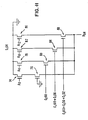
- Figs. 12 and 13 illustrate how scale factor signals S0, S1, S2, S3, S4 and S5 are partially decoded by first and second decoders to provide first and second groups of control signals for controlling the amount of shift or rotate in the mechanisms 10 and 14, respectively.
- the total shift or rotate is the sum of the shift or rotate produced in mechanism 10 at level 1 and mechanism 14 at level 2.
- Mechanism 10 could be at level 2 and mechanism 14 at level 1. In any event, the total amount of shift is the sum of the rotate from each mechanism.
- Fig. 12 illustrates the first decoder 12 which partially decodes the scale factor signals by decoding S2, S3, S4 and S5.
- the complements of these signals are provided by inverters 110, 112, 114, 116 and 118, respectively.
- the codes produced by S2, S3, S4 and S5 are decoded by AND gates 118, 120, 122, 124 and 126 for producing control signals C10, C14, C18, C156 and C160, respectively.
- the AND gates utilized for producing control signals C112, C116, C120, C124, C128, C132 etc through C152 are not shown as their implementation is straight forward.
- Fig. 13 illustrates the second decoder 16 which partially decodes the scale factor signals by decoding S0 and S1. The complements of these signals are provided by inverters 128 and 130 respectively.
- the codes produced by S0 and S1 are decoded by AND gates 132, 134, 136 and 138 to provide the second group of control signals C20, C21, C22 and C23 for controlling the amount of shift or rotate in mechanism 14 at level 2.
- the shifter has been described above in terms of a minimum shift size of one bit position.
- the basic concepts of this invention can be generalized and extended to the case in which the minimum shift size is some power of 2, i.e., 2 c .
- the shift is envisioned as a number to be divided into three sub-fields; "a" most significant bits, "b" middle bits and "c" least significant bits.
- This extension is illustrated in Figs. 14A and 14B, which is similar to Fig. 4 except that all shift amounts are multiplied by 2 c .
- a low order shift distance code (c) can be appended, and the structure can operate as a 2 c base shifter.
- This 2 c shift activity can be performed by a bit level shifter and will not be discussed here.
- the shift amount provided in each level has been multiplied by 2 c .
- the data input to S1q are I(q), I(q - 2 b+c ), I(q - 2 ⁇ 2 b+c ), I(q - 3 ⁇ 2 b+c ).
- the number of OR circuits is limited to the smaller of n and 2 b+c .
- the width of the first level switches is limited to the smaller of 2 a and the least upper bound of (n/2 b+c ).
- Level 2 is similarly modified to include for S2q: S1q, S1(q-2 c ), S1(q-2 ⁇ 2 c ), S1(q-3 ⁇ 2 c ).
- the overflow switches (in the lst level, S1 m..S1m+2 b+c -1 and in the second stage S2m..S2m+2 C ) are modified from the simple shifter form by ORing inputs, and outputs and/or control lines in the manner shown in Figs. 8-11 with suitable adjustments for greater shift distances.
Landscapes
- Engineering & Computer Science (AREA)
- Theoretical Computer Science (AREA)
- Physics & Mathematics (AREA)
- General Engineering & Computer Science (AREA)
- General Physics & Mathematics (AREA)
- Complex Calculations (AREA)
- Compression, Expansion, Code Conversion, And Decoders (AREA)
- Error Detection And Correction (AREA)
- Feedback Control In General (AREA)
Applications Claiming Priority (2)
| Application Number | Priority Date | Filing Date | Title |
|---|---|---|---|
| US07/297,639 US4931970A (en) | 1989-01-13 | 1989-01-13 | Apparatus for determining if there is a loss of data during a shift operation |
| US297639 | 1989-01-13 |
Publications (3)
| Publication Number | Publication Date |
|---|---|
| EP0377845A2 true EP0377845A2 (fr) | 1990-07-18 |
| EP0377845A3 EP0377845A3 (fr) | 1992-05-13 |
| EP0377845B1 EP0377845B1 (fr) | 1995-10-04 |
Family
ID=23147146
Family Applications (1)
| Application Number | Title | Priority Date | Filing Date |
|---|---|---|---|
| EP89122989A Expired - Lifetime EP0377845B1 (fr) | 1989-01-13 | 1989-12-13 | Dispositif de détermination s'il y a une perte de données pendant une opération de décalage |
Country Status (4)
| Country | Link |
|---|---|
| US (1) | US4931970A (fr) |
| EP (1) | EP0377845B1 (fr) |
| JP (1) | JPH02239324A (fr) |
| DE (1) | DE68924479T2 (fr) |
Cited By (1)
| Publication number | Priority date | Publication date | Assignee | Title |
|---|---|---|---|---|
| EP0655675B1 (fr) * | 1993-11-29 | 2000-02-23 | Hewlett-Packard Company | Circuit et méthode de décalage et d'arrondissement |
Families Citing this family (7)
| Publication number | Priority date | Publication date | Assignee | Title |
|---|---|---|---|---|
| JPH03100827A (ja) * | 1989-09-14 | 1991-04-25 | Mitsubishi Electric Corp | オーバフロー検出回路 |
| JP2617252B2 (ja) * | 1991-07-11 | 1997-06-04 | 三田工業株式会社 | プリンタ |
| US5930159A (en) * | 1996-10-17 | 1999-07-27 | Samsung Electronics Co., Ltd | Right-shifting an integer operand and rounding a fractional intermediate result to obtain a rounded integer result |
| US5844827A (en) * | 1996-10-17 | 1998-12-01 | Samsung Electronics Co., Ltd. | Arithmetic shifter that performs multiply/divide by two to the nth power for positive and negative N |
| US5745393A (en) * | 1996-10-17 | 1998-04-28 | Samsung Electronics Company, Ltd. | Left-shifting an integer operand and providing a clamped integer result |
| US5944874A (en) * | 1997-06-23 | 1999-08-31 | Praxair Technology, Inc. | Solid electrolyte ionic conductor systems for the production of high purity nitrogen |
| US5851266A (en) * | 1997-06-23 | 1998-12-22 | Praxair Technology,Inc. | Hybrid solid electrolyte ionic conductor systems for purifying inert gases |
Family Cites Families (3)
| Publication number | Priority date | Publication date | Assignee | Title |
|---|---|---|---|---|
| US4338675A (en) * | 1980-02-13 | 1982-07-06 | Intel Corporation | Numeric data processor |
| JPS5750049A (en) * | 1980-09-09 | 1982-03-24 | Toshiba Corp | Shifting circuit |
| US4396994A (en) * | 1980-12-31 | 1983-08-02 | Bell Telephone Laboratories, Incorporated | Data shifting and rotating apparatus |
-
1989
- 1989-01-13 US US07/297,639 patent/US4931970A/en not_active Expired - Fee Related
- 1989-11-20 JP JP1299893A patent/JPH02239324A/ja active Granted
- 1989-12-13 EP EP89122989A patent/EP0377845B1/fr not_active Expired - Lifetime
- 1989-12-13 DE DE68924479T patent/DE68924479T2/de not_active Expired - Fee Related
Cited By (1)
| Publication number | Priority date | Publication date | Assignee | Title |
|---|---|---|---|---|
| EP0655675B1 (fr) * | 1993-11-29 | 2000-02-23 | Hewlett-Packard Company | Circuit et méthode de décalage et d'arrondissement |
Also Published As
| Publication number | Publication date |
|---|---|
| DE68924479T2 (de) | 1996-05-30 |
| EP0377845B1 (fr) | 1995-10-04 |
| US4931970A (en) | 1990-06-05 |
| JPH02239324A (ja) | 1990-09-21 |
| JPH0429091B2 (fr) | 1992-05-18 |
| EP0377845A3 (fr) | 1992-05-13 |
| DE68924479D1 (de) | 1995-11-09 |
Similar Documents
| Publication | Publication Date | Title |
|---|---|---|
| JP2674754B2 (ja) | バレル・シフタ | |
| Vasudevan et al. | Self-checking carry-select adder design based on two-rail encoding | |
| US5317527A (en) | Leading one/zero bit detector for floating point operation | |
| GB2173022A (en) | A modulo arithmetic unit having arbitrary offset and modulo values | |
| EP0136834A2 (fr) | Circuit numérique exécutant une opération arithmétique avec débordement | |
| US6738795B1 (en) | Self-timed transmission system and method for processing multiple data sets | |
| US5483478A (en) | Method and structure for reducing carry delay for a programmable carry chain | |
| EP0377845B1 (fr) | Dispositif de détermination s'il y a une perte de données pendant une opération de décalage | |
| KR920022095A (ko) | 연산 장치 및 이것을 사용한 비트 필드 조작 연산 방법 | |
| EP0436106B1 (fr) | Additionneur à haute performance et à auto-vérification ayant une faible surface de circuit | |
| JPS62196767A (ja) | パイプライン構成の浮動小数点数アキユムレ−タ回路 | |
| EP0543517B1 (fr) | Circuit pour la détection de la position d'un bit "1" extrême dans un nombre binaire | |
| US5129066A (en) | Bit mask generator circuit using multiple logic units for generating a bit mask sequence | |
| US4349888A (en) | CMOS Static ALU | |
| KR970029772A (ko) | 비트-시리얼 메트릭스 전치를 위한 초대규모 집적회로 | |
| EP0400730B1 (fr) | Dispositif détecteur de passages par zéro | |
| US5126965A (en) | Conditional-sum carry structure compiler | |
| EP0568373B1 (fr) | Appareil et méthode pour la comparaison parallèle de magnitude de données numériques | |
| US5754458A (en) | Trailing bit anticipator | |
| EP0377814A2 (fr) | Décaleur/rotateur à décodage partiel | |
| US6057720A (en) | High speed sticky signal generator | |
| US6522690B1 (en) | Zero determination signal generating circuit | |
| JPH08147142A (ja) | プライオリティ検出用カウンタ装置 | |
| US5018094A (en) | Dual incrementer | |
| US5304994A (en) | Minimal delay leading one detector with result bias control |
Legal Events
| Date | Code | Title | Description |
|---|---|---|---|
| PUAI | Public reference made under article 153(3) epc to a published international application that has entered the european phase |
Free format text: ORIGINAL CODE: 0009012 |
|
| AK | Designated contracting states |
Kind code of ref document: A2 Designated state(s): DE FR GB |
|
| 17P | Request for examination filed |
Effective date: 19901113 |
|
| PUAL | Search report despatched |
Free format text: ORIGINAL CODE: 0009013 |
|
| AK | Designated contracting states |
Kind code of ref document: A3 Designated state(s): DE FR GB |
|
| 17Q | First examination report despatched |
Effective date: 19940307 |
|
| GRAA | (expected) grant |
Free format text: ORIGINAL CODE: 0009210 |
|
| AK | Designated contracting states |
Kind code of ref document: B1 Designated state(s): DE FR GB |
|
| REF | Corresponds to: |
Ref document number: 68924479 Country of ref document: DE Date of ref document: 19951109 |
|
| PGFP | Annual fee paid to national office [announced via postgrant information from national office to epo] |
Ref country code: FR Payment date: 19951128 Year of fee payment: 7 |
|
| PGFP | Annual fee paid to national office [announced via postgrant information from national office to epo] |
Ref country code: DE Payment date: 19951229 Year of fee payment: 7 |
|
| ET | Fr: translation filed | ||
| PLBE | No opposition filed within time limit |
Free format text: ORIGINAL CODE: 0009261 |
|
| STAA | Information on the status of an ep patent application or granted ep patent |
Free format text: STATUS: NO OPPOSITION FILED WITHIN TIME LIMIT |
|
| 26N | No opposition filed | ||
| PGFP | Annual fee paid to national office [announced via postgrant information from national office to epo] |
Ref country code: GB Payment date: 19961126 Year of fee payment: 8 |
|
| PG25 | Lapsed in a contracting state [announced via postgrant information from national office to epo] |
Ref country code: FR Effective date: 19970829 |
|
| PG25 | Lapsed in a contracting state [announced via postgrant information from national office to epo] |
Ref country code: DE Effective date: 19970902 |
|
| REG | Reference to a national code |
Ref country code: FR Ref legal event code: ST |
|
| PG25 | Lapsed in a contracting state [announced via postgrant information from national office to epo] |
Ref country code: GB Free format text: LAPSE BECAUSE OF NON-PAYMENT OF DUE FEES Effective date: 19971213 |
|
| GBPC | Gb: european patent ceased through non-payment of renewal fee |
Effective date: 19971213 |