EP0377940A2 - Verbindungshalbleiter, denselben anwendendes Halbleiter-Bauelement und Herstellungsverfahren des Halbleiter-Bauelementes - Google Patents
Verbindungshalbleiter, denselben anwendendes Halbleiter-Bauelement und Herstellungsverfahren des Halbleiter-Bauelementes Download PDFInfo
- Publication number
- EP0377940A2 EP0377940A2 EP89310004A EP89310004A EP0377940A2 EP 0377940 A2 EP0377940 A2 EP 0377940A2 EP 89310004 A EP89310004 A EP 89310004A EP 89310004 A EP89310004 A EP 89310004A EP 0377940 A2 EP0377940 A2 EP 0377940A2
- Authority
- EP
- European Patent Office
- Prior art keywords
- layer
- type
- superlattice
- substrate
- compound semiconductor
- Prior art date
- Legal status (The legal status is an assumption and is not a legal conclusion. Google has not performed a legal analysis and makes no representation as to the accuracy of the status listed.)
- Granted
Links
Images






Classifications
-
- H—ELECTRICITY
- H10—SEMICONDUCTOR DEVICES; ELECTRIC SOLID-STATE DEVICES NOT OTHERWISE PROVIDED FOR
- H10H—INORGANIC LIGHT-EMITTING SEMICONDUCTOR DEVICES HAVING POTENTIAL BARRIERS
- H10H20/00—Individual inorganic light-emitting semiconductor devices having potential barriers, e.g. light-emitting diodes [LED]
- H10H20/80—Constructional details
- H10H20/81—Bodies
- H10H20/822—Materials of the light-emitting regions
- H10H20/824—Materials of the light-emitting regions comprising only Group III-V materials, e.g. GaP
- H10H20/825—Materials of the light-emitting regions comprising only Group III-V materials, e.g. GaP containing nitrogen, e.g. GaN
-
- B—PERFORMING OPERATIONS; TRANSPORTING
- B82—NANOTECHNOLOGY
- B82Y—SPECIFIC USES OR APPLICATIONS OF NANOSTRUCTURES; MEASUREMENT OR ANALYSIS OF NANOSTRUCTURES; MANUFACTURE OR TREATMENT OF NANOSTRUCTURES
- B82Y20/00—Nanooptics, e.g. quantum optics or photonic crystals
-
- H—ELECTRICITY
- H01—ELECTRIC ELEMENTS
- H01S—DEVICES USING THE PROCESS OF LIGHT AMPLIFICATION BY STIMULATED EMISSION OF RADIATION [LASER] TO AMPLIFY OR GENERATE LIGHT; DEVICES USING STIMULATED EMISSION OF ELECTROMAGNETIC RADIATION IN WAVE RANGES OTHER THAN OPTICAL
- H01S5/00—Semiconductor lasers
- H01S5/30—Structure or shape of the active region; Materials used for the active region
- H01S5/32—Structure or shape of the active region; Materials used for the active region comprising PN junctions, e.g. hetero- or double- heterostructures
- H01S5/323—Structure or shape of the active region; Materials used for the active region comprising PN junctions, e.g. hetero- or double- heterostructures in AIIIBV compounds, e.g. AlGaAs-laser, InP-based laser
- H01S5/32308—Structure or shape of the active region; Materials used for the active region comprising PN junctions, e.g. hetero- or double- heterostructures in AIIIBV compounds, e.g. AlGaAs-laser, InP-based laser emitting light at a wavelength less than 900 nm
- H01S5/32341—Structure or shape of the active region; Materials used for the active region comprising PN junctions, e.g. hetero- or double- heterostructures in AIIIBV compounds, e.g. AlGaAs-laser, InP-based laser emitting light at a wavelength less than 900 nm blue laser based on GaN or GaP
-
- H—ELECTRICITY
- H01—ELECTRIC ELEMENTS
- H01S—DEVICES USING THE PROCESS OF LIGHT AMPLIFICATION BY STIMULATED EMISSION OF RADIATION [LASER] TO AMPLIFY OR GENERATE LIGHT; DEVICES USING STIMULATED EMISSION OF ELECTROMAGNETIC RADIATION IN WAVE RANGES OTHER THAN OPTICAL
- H01S5/00—Semiconductor lasers
- H01S5/30—Structure or shape of the active region; Materials used for the active region
- H01S5/34—Structure or shape of the active region; Materials used for the active region comprising quantum well or superlattice structures, e.g. single quantum well [SQW] lasers, multiple quantum well [MQW] lasers or graded index separate confinement heterostructure [GRINSCH] lasers
- H01S5/343—Structure or shape of the active region; Materials used for the active region comprising quantum well or superlattice structures, e.g. single quantum well [SQW] lasers, multiple quantum well [MQW] lasers or graded index separate confinement heterostructure [GRINSCH] lasers in AIIIBV compounds, e.g. AlGaAs-laser, InP-based laser
-
- H—ELECTRICITY
- H10—SEMICONDUCTOR DEVICES; ELECTRIC SOLID-STATE DEVICES NOT OTHERWISE PROVIDED FOR
- H10H—INORGANIC LIGHT-EMITTING SEMICONDUCTOR DEVICES HAVING POTENTIAL BARRIERS
- H10H20/00—Individual inorganic light-emitting semiconductor devices having potential barriers, e.g. light-emitting diodes [LED]
- H10H20/01—Manufacture or treatment
- H10H20/011—Manufacture or treatment of bodies, e.g. forming semiconductor layers
- H10H20/013—Manufacture or treatment of bodies, e.g. forming semiconductor layers having light-emitting regions comprising only Group III-V materials
-
- H—ELECTRICITY
- H10—SEMICONDUCTOR DEVICES; ELECTRIC SOLID-STATE DEVICES NOT OTHERWISE PROVIDED FOR
- H10H—INORGANIC LIGHT-EMITTING SEMICONDUCTOR DEVICES HAVING POTENTIAL BARRIERS
- H10H20/00—Individual inorganic light-emitting semiconductor devices having potential barriers, e.g. light-emitting diodes [LED]
- H10H20/01—Manufacture or treatment
- H10H20/011—Manufacture or treatment of bodies, e.g. forming semiconductor layers
- H10H20/013—Manufacture or treatment of bodies, e.g. forming semiconductor layers having light-emitting regions comprising only Group III-V materials
- H10H20/0133—Manufacture or treatment of bodies, e.g. forming semiconductor layers having light-emitting regions comprising only Group III-V materials with a substrate not being Group III-V materials
- H10H20/01335—Manufacture or treatment of bodies, e.g. forming semiconductor layers having light-emitting regions comprising only Group III-V materials with a substrate not being Group III-V materials the light-emitting regions comprising nitride materials
-
- H—ELECTRICITY
- H10—SEMICONDUCTOR DEVICES; ELECTRIC SOLID-STATE DEVICES NOT OTHERWISE PROVIDED FOR
- H10H—INORGANIC LIGHT-EMITTING SEMICONDUCTOR DEVICES HAVING POTENTIAL BARRIERS
- H10H20/00—Individual inorganic light-emitting semiconductor devices having potential barriers, e.g. light-emitting diodes [LED]
- H10H20/01—Manufacture or treatment
- H10H20/011—Manufacture or treatment of bodies, e.g. forming semiconductor layers
- H10H20/018—Bonding of wafers
-
- H—ELECTRICITY
- H10—SEMICONDUCTOR DEVICES; ELECTRIC SOLID-STATE DEVICES NOT OTHERWISE PROVIDED FOR
- H10H—INORGANIC LIGHT-EMITTING SEMICONDUCTOR DEVICES HAVING POTENTIAL BARRIERS
- H10H20/00—Individual inorganic light-emitting semiconductor devices having potential barriers, e.g. light-emitting diodes [LED]
- H10H20/80—Constructional details
- H10H20/81—Bodies
- H10H20/811—Bodies having quantum effect structures or superlattices, e.g. tunnel junctions
-
- H—ELECTRICITY
- H10—SEMICONDUCTOR DEVICES; ELECTRIC SOLID-STATE DEVICES NOT OTHERWISE PROVIDED FOR
- H10H—INORGANIC LIGHT-EMITTING SEMICONDUCTOR DEVICES HAVING POTENTIAL BARRIERS
- H10H20/00—Individual inorganic light-emitting semiconductor devices having potential barriers, e.g. light-emitting diodes [LED]
- H10H20/80—Constructional details
- H10H20/81—Bodies
- H10H20/811—Bodies having quantum effect structures or superlattices, e.g. tunnel junctions
- H10H20/812—Bodies having quantum effect structures or superlattices, e.g. tunnel junctions within the light-emitting regions, e.g. having quantum confinement structures
-
- H—ELECTRICITY
- H01—ELECTRIC ELEMENTS
- H01S—DEVICES USING THE PROCESS OF LIGHT AMPLIFICATION BY STIMULATED EMISSION OF RADIATION [LASER] TO AMPLIFY OR GENERATE LIGHT; DEVICES USING STIMULATED EMISSION OF ELECTROMAGNETIC RADIATION IN WAVE RANGES OTHER THAN OPTICAL
- H01S5/00—Semiconductor lasers
- H01S5/30—Structure or shape of the active region; Materials used for the active region
- H01S5/34—Structure or shape of the active region; Materials used for the active region comprising quantum well or superlattice structures, e.g. single quantum well [SQW] lasers, multiple quantum well [MQW] lasers or graded index separate confinement heterostructure [GRINSCH] lasers
- H01S5/343—Structure or shape of the active region; Materials used for the active region comprising quantum well or superlattice structures, e.g. single quantum well [SQW] lasers, multiple quantum well [MQW] lasers or graded index separate confinement heterostructure [GRINSCH] lasers in AIIIBV compounds, e.g. AlGaAs-laser, InP-based laser
- H01S5/34333—Structure or shape of the active region; Materials used for the active region comprising quantum well or superlattice structures, e.g. single quantum well [SQW] lasers, multiple quantum well [MQW] lasers or graded index separate confinement heterostructure [GRINSCH] lasers in AIIIBV compounds, e.g. AlGaAs-laser, InP-based laser with a well layer based on Ga(In)N or Ga(In)P, e.g. blue laser
-
- Y—GENERAL TAGGING OF NEW TECHNOLOGICAL DEVELOPMENTS; GENERAL TAGGING OF CROSS-SECTIONAL TECHNOLOGIES SPANNING OVER SEVERAL SECTIONS OF THE IPC; TECHNICAL SUBJECTS COVERED BY FORMER USPC CROSS-REFERENCE ART COLLECTIONS [XRACs] AND DIGESTS
- Y10—TECHNICAL SUBJECTS COVERED BY FORMER USPC
- Y10S—TECHNICAL SUBJECTS COVERED BY FORMER USPC CROSS-REFERENCE ART COLLECTIONS [XRACs] AND DIGESTS
- Y10S148/00—Metal treatment
- Y10S148/065—Gp III-V generic compounds-processing
-
- Y—GENERAL TAGGING OF NEW TECHNOLOGICAL DEVELOPMENTS; GENERAL TAGGING OF CROSS-SECTIONAL TECHNOLOGIES SPANNING OVER SEVERAL SECTIONS OF THE IPC; TECHNICAL SUBJECTS COVERED BY FORMER USPC CROSS-REFERENCE ART COLLECTIONS [XRACs] AND DIGESTS
- Y10—TECHNICAL SUBJECTS COVERED BY FORMER USPC
- Y10S—TECHNICAL SUBJECTS COVERED BY FORMER USPC CROSS-REFERENCE ART COLLECTIONS [XRACs] AND DIGESTS
- Y10S148/00—Metal treatment
- Y10S148/113—Nitrides of boron or aluminum or gallium
Definitions
- the present invention relates to a compound semiconductor material having a large band gap which can be effectively used for a short wavelength light-emitting element, a semiconductor element using the same, and a method of manufacturing the semiconductor element.
- nitrides and phosphides of light Group III elements have large band gaps, e.g., BN (4 or 8 eV), AlN (6 eV), GaN (3.4 eV), InP (2.4 eV), AlP (2.4 eV), and GaP (2.3 and 2.8 eV).
- BN has a large band gap, but a high-pressure phase (c-BN) of BN having a 4-coordinate (sp3) bond is difficult to synthesize.
- c-BN high-pressure phase
- sp3 4-coordinate
- InN has a relatively small band gap and poor thermal stability. Generally, only polycrystals can be obtained from InN. The band gaps of both AlP and GaP are slightly insufficient. Other compounds, i.e., AlN and GaN have large band gaps and are excellent in stability. Therefore, AlN and GaN are suitable for short wavelength light-emitting elements. However, AlN and GaN have Worzeite type (to be referred as a WZ type) crystal structures. In addition, since GaN has a strong ionization tendency, lattice defects tend to occur. Therefore, a p-type semiconductor having a low resistance cannot be obtained from GaN.
- Fig. 1A shows a band structure of a cubic semiconductor.
- the ⁇ point is set at the bottom of a conduction band for convenience.
- Degeneracy of bands of heavy and light holes occurs near the apex of a valence band of interest.
- an orbit which is shifted to the low energy side due to spin-orbit interaction is present in the valence band.
- the average mass of the holes in the two bands is regarded as an effective mass.
- the WZ structure of a hexagonal crystal is greatly influenced by a crystalline field due to its strong uniaxial isotropy. As shown in Fig.
- no conventional semiconductor material can satisfy the conditions required for realizing a green emission semiconductor laser or a high-luminance blue LED, i.e., having a sufficiently large band gap, e.g., 2.7 eV, allowing easy p-n junction control, and being excellent in crystal quality.
- a sufficiently large band gap e.g., 2.7 eV
- AlN and GaN are nitrides which are effective in obtaining large band gaps, low-resistance p-type layers cannot be obtained.
- a Ga x Al 1-x N (0 ⁇ x ⁇ 1) layer is stacked on a BP layer having substantially the same bond length as that thereof, a ZB structure, and a small ionization tendency, and allowing easy p-n junction control so as to form a heterojunction, thereby providing a compound semiconductor material of a ZB structure which has both a large band gap property of a direct transition type nitride and the characteristics of BP, i.e., having a small ionization tendency and free from defects.
- the present invention is characterized in that a semiconductor element is formed by using a Ga x Al 1-x N layer which is processed in the above-described manner to have a ZB type crystal structure.
- a metal organic chemical vapor deposition apparatus having a plurality of reaction tubes is used, and a substrate is moved between the reaction tubes so as to sequentially grow a BP layer and a Ga x Al 1-x N layer on the substrate, thereby forming a heterojunction.
- a Ga x Al 1-x N having a ZB structure by growing a Ga x Al 1-x N layer on a BP layer having a ZB structure, a Ga x Al 1-x N having a ZB structure can be obtained. Therefore, an excellent compound semiconductor material having a large band gap, allowing easy p-n junction control, and having good crystal quality can be obtained. Similarly, if a mixed crystal is manufactured by mixing GaN, Al, and BP, an excellent compound semiconductor material of a ZB structure having a large band gap can be obtained. A light-emitting element for emitting light of a short wavelength which is shorter than that of green light can be realized by using these materials.
- a metal organic chemical vapor deposition apparatus having a plurality of reaction tubes is used, and a substrate is moved between these reaction tubes so that the respective source gases can alternately be fed onto the substrate with abrupt changes in concentration within a very short period of time.
- BP layers and Ga x Al 1-x N layers can be alternately stacked on the substrate at a desired stacking cycle, thus obtaining an element wafer having a multilayer structure.
- Fig. 2 shows a semiconductor wafer having a superlattice structure of GaN/BP according to an embodiment of the present invention.
- a GaP layer 2 as a buffer layer is formed on a GaP substrate 1.
- BP layers 3 and GaN layers 4 are alternately stacked on the GaP layer 2 at a predetermined cycle.
- Fig. 3 shows a metal organic chemical vapor deposition (MOCVD) apparatus of a multi-chamber system used to manufacture such a superlattice structure semiconductor wafer.
- reference numerals 11, 12, and 13 denote quartz reaction tubes.
- Required source gases are respectively fed into the reaction tubes 11, 12, and 13 through gas feed ports respectively arranged at their upper portions.
- These reaction tubes 11, 12, and 13 are vertically mounted on a chamber 14 so as to extend through the upper lid of the chamber 14.
- a substrate 15 is placed a graphite susceptor 16. More specifically, the substrate 15 is placed on the susceptor 16 so as to oppose the openings of the reaction tubes 11, 12, and 13, and is heated to a high temperature by an external high-frequency coil 17.
- the susceptor 16 is mounted on a quartz holder 18.
- the susceptor 16 can be moved by a driving shaft through a magnetic fluid seal at high speed under the reaction tubes 11, 12, and 13. This driving operation is performed by a computer-controlled motor which is arranged outside the apparatus.
- a thermocouple 20 is arranged at the central portion of the susceptor 16. The thermocouple 20 monitors temperatures immediately under the substrate and extracts them.
- a slip ring is used for a code portion of the thermocouple 20 so as to prevent a twist due to rotation.
- a reacted gas is pushed by a fast downflow of a hydrogen gas flowing from an upper injection port 21 and is exhausted from an exhaust port 22 by a rotary pump so as to suppress mixing of the gases.
- a semiconductor wafer shown in Fig. 2 in detail was manufactured by using the MOCVD apparatus shown in Fig. 3.
- the properties of a crystal layer of the manufactured wafer were checked. The results will be described below.
- the source gases used were: trimethyl gallium (TMG) of a methyl-based organic metal, trimethyl aluminum (TMA), diborane (B2H6), or triethyl boron (TEB); phosphine (PH3); and ammonia (NH3).
- TMG trimethyl gallium
- TMA trimethyl aluminum
- B2H6 diborane
- TEB triethyl boron
- PH3 phosphine
- NH3 ammonia
- the temperature of the substrate 15 was set at 850 to 1,150°C; the pressure, 0.3 atm; and the total flow rate of the source gases, 1 l/min.
- the gas flow rates were determined to set the growth rate at 1 ⁇ m/h.
- the flow rates of the respective source gases were: 1 ⁇ 10 ⁇ 6 mol/min for TEB; 1 ⁇ 10 ⁇ 6 mol/min for TMG; 5 ⁇ 10 ⁇ 4 mol/min for PH3; and 1 ⁇ 10 ⁇ 3 mol/min for NH3.
- the stacking cycle was 50 to 300 ⁇ .
- a superlattice layer exhibits an n conductivity type without doping.
- Zn was doped by mixing dimethylzinc (DMZ) with the source gases, a p-type crystal was obtained.
- DMZ dimethylzinc
- a carrier concentration as well as a conductivity type could be controlled by changing the amount of DMZ.
- a steep heterojunction of a nitride (GaAlN, GaN, and AlN) and a phosphide (BP), which was difficult to form in the past, can be formed. Therefore, a compound semiconductor wafer of a ZB structure allowing easy p-n junction control and having a large band gap (2.7 eV) can be obtained. A high-luminance blue LED and a green light semiconductor laser can be formed by using this semiconductor wafer.
- Fig. 4 shows a semiconductor wafer according to another embodiment of the present invention.
- a Ga x Al y B 1-x-y N z P 1-z layer 5 as a mixed crystal is grown on a GaP substrate 1 through a GaP layer 2 as a buffer layer.
- Fig. 5 shows an MOCVD apparatus for manufacturing the semiconductor wafer shown in Fig. 4.
- Reference numeral 23 denotes a quartz reaction tube. Source gases are fed from a gas feed port 24 located at the upper portion of the reaction tube 23. Gases in the reaction tube 23 are exhausted from an exhaust port 25.
- a substrate 27 is mounted on a graphite susceptor 26 and is arranged in the reaction tube 23. The substrate 27 is induction-heated by an external high-frequency coil 28.
- Reference numeral 29 denotes a thermocouple for detecting the temperature of the susceptor 26.
- a GaP layer 2 was grown on a GaP substrate 1, and a Ga x Al y B 1-x-y N z P 1-z (0 ⁇ x, y, z ⁇ 1) was grown on the resultant structure by using the MOCVD apparatus shown in Fig. 5.
- the source gases were: trimethyl gallium (TMG) of a methyl-based organic metal, trimethyl aluminum (TMA), diborane (B2H6), or triethyl boron (TEB); phosphine (PH3); and ammonia (NH3).
- TMG trimethyl gallium
- TMA trimethyl aluminum
- B2H6 diborane
- TEB triethyl boron
- PH3 phosphine
- NH3 ammonia
- a mixed crystal layer consisting of BP and GaAlN which has a large band gap, allows easy p-n junction control, and is excellent in crystal quality can be obtained.
- Fig. 6 shows an embodiment in which an LED employs a GaAlN/BP superlattice layer.
- An Si-doped n-type BP layer 32 is grown on an Si-doped n-type GaP substrate 31 to a thickness of about 2 ⁇ m.
- An Si-doped n-type GaAlN/BP superlattice layer 33 having a thickness of about 3 ⁇ m and a Mg-doped p-type GaAln/BP superlattice layer 34 having a thickness of about 2 ⁇ m are sequentially grown on the BP layer 32. Crystal growth is performed by the MOCVD apparatus shown in Fig. 3.
- the superlattice layers 33 and 34 are formed by alternately stacking Ga 0.5 Al 0.5 N and BP layers, and hence layers having a thickness of 10 ⁇ + 10 ⁇ are repeatedly stacked.
- the n-type superlattice layer 33 is formed by using silane (SiH4) as a dopant so as to have a carrier concentration of 1 ⁇ 1017 atoms/cm3, whereas the p-type superlattice layer 34 is formed by using cyclopentadienyl magnesium (CP2Mg) as a dopant so as to have a carrier concentration of 2 ⁇ 1016 atoms/cm3.
- In (indium) electrodes 35 and 36 are respectively formed on the upper and lower surfaces of the element wafer.
- Fig. 7 shows an embodiment in which a DH laser is formed by using a GaAlN/BP superlattice layer. Similar to the above-described embodiment, in this embodiment, the MOCVD apparatus shown in Fig. 3 is used to form the superlattice layer. More specifically, an Si-doped n-type BP layer 42 as a buffer layer is formed on an n-type GaP substrate 41. An Si-doped n-type GaAlN/BP superlattice layer 43 is grown on the BP layer 42 to a thickness of about 1 ⁇ m, and an undoped GaAlN superlattice layer 44 is grown on the resultant structure to a thickness of about 0.1 ⁇ m.
- an Mg-doped p-type GaAlN/BP superlattice layer 45 is grown on the resultant structure to a thickness of about 1 ⁇ m.
- the undoped superlattice layer 44 serves as an active layer.
- Each of the superlattice layers 43 to 45 has a composition of Ga 0.5 Al 0.5 N and BP layers which are alternately stacked.
- Each of the p- and n-type superlattice layers 45 and 43 is formed at a cycle of 7 ⁇ + 13 ⁇ , i.e., 20 ⁇ and has a band gap of about 3.0 eV.
- the undoped superlattice layer 44 is formed at a cycle of 5 ⁇ + 5 ⁇ , i.e., 10 ⁇ and has a band gap of 2.7 eV.
- the n-type superlattice layer 43 is formed upon doping of Si using SiH4 and has a carrier concentration of 1 ⁇ 1017 atoms/cm3.
- the p-type superlattice layer 45 is formed upon doping of MB using CP2Mg and has a carrier concentration of 1 ⁇ 1017 atoms/cm3.
- In (indium) electrodes 46 and 47 are formed on the upper and lower surfaces of the resultant structure, respectively.
- Blue emission can be realized by the DH layer of this embodiment.
- Tl, and the like as Group III elements may be mixed in place of Ga, Al, and B, and As, Sb, Bi, and the like may be mixed as Group V elements.
- As source gases triethyl gallium (TEA) can be used for Ga; an ethyl group organic metal such as triethyl aluminum (TEA), for Al; and trimethyl boron (TMB), for B.
- a nitrogen gas, hydrazine (N2H4), or an organic matal compound called an adduct such as Ga(C2H5)3 ⁇ NH3, Ga(CH3)3 ⁇ N ⁇ (CH3), Al(C2H5)3 ⁇ NH3, or Al(CH3)3 ⁇ N ⁇ (CH3)3 may be used.
- the compound semiconductor materials of the present invention i.e., a GaAlN and BP superlattice structure semiconductor or a mixed crystal semiconductor of Ga x Al y B 1-x-y N z P 1-z is is composed of a combination of direct and indirect transition types and a combination of WZ and ZB structures having different characteristics. For this reason, problems posed in such a material are that the bond lengths of Al-N and B-N are especially short as compared with other bond lengths, and AlN has a high resistance. As described above, in order to allow stable existence of this semiconductor material, it is essential that x + y is substantially equal to z .
- AlN and GaN have large band gaps of 6.2 eV and 3.4 eV, respectively, and are of direct transition type, they are preferably used for formation of p-n junctions.
- both crystals of AlN and GaN have WZ structures.
- a compound BP of B and P which are the remaining constituent elements has a small band gap of about 2.0 eV and is of an indirect transition type.
- it has a ZB structure. Therefore, the lower limit of B and P as ZB type compounds which is necessary to keep a crystal to be of a ZB type is determined. According to the experiments performed by the present inventors, it was required that the lower limit of B and P components was 0.2, i.e., x + y ⁇ z ⁇ 0.8. If it exceeds 0.2, some crystals started exhibiting a WZ structure.
- BP is of an indirect transition type which has a valence band at the X point.
- Al is of a direct transition type which has the bottom of a valence band at the ⁇ point.
- Fig. 8 shows changes in band gap and position of the bottom of a valence band based on the composition of a mixed crystal expected from these materials. More specifically, Fig. 8 shows changes in band structure due to two pseudo two-element composition (Al a N a B 1-a P 1-a , Ga b N b B 1-b P 1-b ; 0 ⁇ a, b ⁇ 1) of BP and AlN, and BP and GaN. Referring to Fig.
- reference symbols X, ⁇ , and A denote positions of the bottoms of valence bands. Such a linear approximation is considered as a satisfactorily accurate approximation in a mixed crystal of GaAs-AlAs.
- a laser which can perform stable oscillation has not been realized by indirect transition type materials.
- direct transition type materials In order to realize light-emitting elements, it is important to use direct transition type materials. Therefore, the ratio of a nitride component to a boride component is set to be large to convert an indirect transition type material to a direct transition type material. It is apparent from Fig. 8 that a band structure is substantially determined on the basis of the value x + y, and that a band structure does not much depend on the ratio of x to y .
- an average composition falls in the range of 0.6 ⁇ x + y ⁇ z, in which the content of a nitride is large.
- the component ratio of Group III elements must be considered. If the concentration of Al is increased, an AlN component is increased in amount to effectively increase a band gap. However, AlN has a small lattice constant or bond length as compared with GaN and BP. Therefore, AlN is not preferable in terms of lattice matching. In addition, AlN has generally a high resistivity of 1010 ⁇ cm or more, and hence poses a problem as a constituent element. When a mixed crystal is to be formed by using AlN, if a bond of Al-P is formed, a cubic crystal having a low resistance can be formed. However, it has a long bond length of 2.36 ⁇ . This may lead to formation of an unstable indirect transition type compound AlP, and hence an increase in Al concentration is not desirable.
- Fig. 9 shows changes in bond length of a mixed crystal AlGaN with respect to a composition.
- mismatching of bond lengths reaches 2% with respect to BP. Therefore, a content y of Al need be limited to about y ⁇ 2x.
- Fig. 10 shows a GaAlN/BP superlattice structure wafer of such an embodiment.
- the MOCVD apparatus shown in Fig. 3 was used to manufacture this superlattice structure wafer.
- a GaP layer 52 as a buffer layer was formed on a GaP substrate 51.
- BP and GaAlN layers 53 and 54 were alternately stacked on the GaP layer 52.
- the stacking cycle was set to be 50 to 300 ⁇ .
- the thicknesses of the BP and GaAlN layers 53 and 54 were set as 1 : 1.
- the source gases were: trimethyl aluminum (TMA); trimethyl gallium (TMG); triethyl boron (TEB); ammonia (NH3); and phosphine (PH3).
- the substrate temperature was set to be 850 to 1,150°C; the pressure, 0.3 atm; and the total flow rate of the source gases, 1 l/min.
- the gas flow rates were set so as to set a growth rate of 1 ⁇ m/h.
- the approximate gas flow rates were: TMA: 1 ⁇ 10 ⁇ 6 mol/min; TMG: 1 ⁇ 10 ⁇ 6 mol/min; TEB: 1 ⁇ 10 ⁇ 6 mol/min; PH3: 5 ⁇ 1014 mol/min; and NH3: 1 ⁇ 10 ⁇ 3 mol/min.
- Doping was performed by mixing silane (SiH4) and cyclopentadienyl magnesium (CP2Mg) with the source gases.
- the properties of the obtained superlattice structure wafer were measured.
- the layer In hole measurement of an undoped GaN layer which was grown in a preliminary step, the layer exhibited an n conductivity type having a carrier concentration of 1 ⁇ 1016 atoms/cm3 and a hole mobility of about 150 cm2/V sec. That is, it was confirmed that the number of holes of N atoms was very small.
- the AlN layer exhibited a high resistivity of 1 ⁇ 106 ⁇ cm or more.
- Fig. 11 shows changes in resistivity ⁇ of this superlattice structure due to its Al composition. It is apparent from Fig. 11 that the ratio of the content of Al to that of Ga should be limited to 2 : 1 at maximum.
- Fig. 12 shows results obtained by checking changes in resistivity when only a staking cycle is changed while the composition ratio of a nitrogen layer is fixed to Ga 0.5 Al 0.5 N. If the stacking cycle is very small, i.e., a layer having a thickness corresponding to a few atoms, the effects of structural disturbance or defects are strong. In this case, the resistance tends to be large. Generally, the resistance is almost equal to that of a single GaN layer. However, the resistance begins to increase at a stacking cycle of about 50 ⁇ , and reaches three times larger than that of a layer of a short cycle at 100 ⁇ . This may be because electrons are locally present in one of the layers.
- a band gap can be changed while lattice constants are kept unchanged. Therefore, it is considered that a semiconductor layer having required characteristics can be obtained by predicting and growing a composition and stacking structure on the basis of the principle of the present invention by using the apparatus shown in Fig. 3. However, it is found from formation of a multilayer wafer that a semiconductor layer having a large band gap cannot necessarily be obtained from an arbitrary composition and an arbitrary stacking structure.
- Fig. 13 shows a sectional structure of a single-heterojunction type LED which is prepared as a sample by using the above-described superlattice structure semiconductor.
- a p-type BP layer 62 having a thickness of 2 ⁇ m and a carrier concentration of 3 ⁇ 1017 atoms/cm3 as a buffer layer is formed on a Zn-doped p-type GaP substrate 61 having a carrier concentration of 5 ⁇ 1017 atoms/cm3.
- a p-type Al 0.5 Ga 0.5 N/BP superlattice layer 63 having a thickness of 2 ⁇ m and a carrier concentration 1 ⁇ 1017 atoms/cm3 and an n-type Al 0.5 Ga 0.5 N/BP superlattice layer 64 having a thickness of 2 ⁇ m and a carrier concentration of 1 ⁇ 1016 atoms/cm3 are sequentially formed on the resultant structure.
- a film thickness ratio r of a superlattice layer at this portion the band gap is changed.
- An n-type GaN layer 65 as a contact layer is formed on the resultant structure.
- Ohmic electrodes 66 and 67 are formed on the upper and lower surface of the LED.
- Fig. 14 shows changes in luminance of the LED thus obtained due to an average composition ratio z .
- a superlattice structure is realized by using the nitrogen composition ratio z as a parameter.
- Almost no light emission occurs in the range in which the value z is small, and an indirect transition BP layer occupies most of the region of the LED.
- the reason why the luminance is decreased in this manner is that some crystals are converted into a WZ structure, and an excellent p-type crystal cannot be obtained. More specifically, in this range, it is difficult to form a p-type crystal having a low resistance.
- peaks representing a ZB structure become obscure, and reflection due to a WZ structure will be actually recognized.
- At z 0.85 or more, most of the crystals are converted into a WZ structure, and hence no p-type layer can obtained, and no light emission is not recognized.
- Fig. 15 is a sectional view of a double-heterojunction (DH) type laser employing a superlattice structure similar to the one described above.
- An Si-doped p-type BP buffer layer 72 having a carrier concentration of 5 ⁇ 1017 atoms/cm3 is formed on an Si-doped n-type GaP substrate 71 having a carrier concentration of 1 ⁇ 1018 atoms/cm3 so as to have a thickness of 2 ⁇ m.
- an n-type BP layer Si doping; carrier concentration: 2 ⁇ 1017 atoms/cm3; 1 ⁇ m
- a p-type BP layer Mg doping; carrier concentration: 5 ⁇ 1017 atoms/cm3, 77 as a contact layer is formed on the resultant structure.
- Ohmic electrodes 78 and 79 are formed on the upper and lower surfaces of the resultant structure, thus completing a DH laser.
- the threshold value is at about 100 KA/cm2.
- the LED and DH laser employ superlattice semiconductors to form light-emitting layers, and the film thickness ratio r is changed while the composition ratio of Al to Ga and the stacking cycle of each superlattice layer are fixed in order to change band gaps.
- the band gaps can be more easily changed by changing the composition ratio of Al to Ga. In this case, if the Al concentration is simply increased, only a high-resistance n-type layer can be obtained. If the band gaps are to be changed by this method, the content of nitride components must be decreased to a certain value.
- the superlattice layer semiconductor may be substituted by a mixed crystal semiconductor having a composition of Ga x Al y B 1-x-y N z P 1-z (0 ⁇ x, y, x + y ⁇ z) of a ZB type.
- a mixed crystal semiconductor having a composition of Ga x Al y B 1-x-y N z P 1-z (0 ⁇ x, y, x + y ⁇ z) of a ZB type.
- the hole mobility was as low as about 50 cm2/V ⁇ sec.
- a light-emitting element is to be formed by using new compound semiconductor materials of the present invention
- selection of a substrate which is transparent to emission wavelengths and allows lattice matching is difficult. For this reason, light extraction efficiency is undesirably degraded due to light absorption of a substrate.
- a stress acts on a light-emitting layer due to lattice mismatching.
- Fig. 18 shows an LED having a double-heterojunction structure according to one of the above embodiments.
- This LED comprises a double-heterojunction structure consisting of a p-type AlGaN/BP superlattice layer 81, an undoped AlGaN/BP superlattice layer 82, and an n-type AlGaN/BP superlattice layer 83, and a thick n-type AlGaN contact layer 84 having a WZ structure formed on the double-heterojunction structure.
- Ohmic electrodes 85 and 86 are respectively formed on the n- and p-type layer sides.
- This LED is manufactured by using the MOCVD apparatus shown in Fig. 3. The manufacturing steps will be described in detail below.
- the source gases were: TMA, TMG, TEB, NH3, and PH3.
- the substrate temperature was set at 850 to 1,150°C; the pressure, 0.3 atm; and the total flow rate of the source gases, 1 l/min.
- the respective gas flow rates were set for a growth rate of 1 ⁇ m/h.
- the flow rates of the respective source gases were: TMA: 1 ⁇ 10 ⁇ 6 mol/min; TMG: 1 ⁇ 10 ⁇ 6 mol/min; TEB: 1 ⁇ 10 ⁇ 6 mol/min; PH3: 5 ⁇ 10 ⁇ 4 mol/min; and NH3: 1 ⁇ 10 ⁇ 3 mol/min.
- Si and Mg were respectively used as n- and p-type dopants.
- Si was doped by mixing silane (SiH4) with a source gas
- Mg was doped by mixing cyclopentadienyl magnesium (CP2Mg) with a source gas.
- a 0.1- ⁇ m thick p-type BP buffer layer is formed on a Zn-doped p-type GaP substrate.
- a p-type AlGaN/BP superlattice layer 81 carrier concentration: 1 ⁇ 1017 atoms/cm3; thickness: 2 ⁇ m; band gap: 3.0 eV
- an undoped AlGaN/BP superlattice layer 82 thickness: 0.5 ⁇ m; band gap: 2.7 eV
- an n-type AlGaN/BP superlattice layer 83 are sequentially grown on the buffer layer.
- a portion having a band gap of 3.9 eV consists of Al 0.5 Ga 0.5 N (13 ⁇ )/BP (7 ⁇ ), and an undoped portion having a band gap of 2.7 eV consists of Al 0.5 Ga 0.5 N (10 ⁇ )/BP (10 ⁇ ).
- This stacked portion is formed at a stacking cycle of 20 ⁇ .
- a contact layer 84 carrier concentration: 5 ⁇ 1017 atoms/cm3; band gap: 3.4 eV
- an Si-doped n-type AlGaN is grown on the DH structure to a thickness of 30 ⁇ m.
- This contact layer 84 has a ZB structure near the interface with the n-type AlGaN/BP layer 83. However, if the layer 84 is grown thick, its most part becomes a WZ type. This layer is transparent to emission wavelengths. In addition, this layer has a high growth rate, and hence is suitable for a thick layer such as a contact layer.
- the GaP substrate side is polished and etched by using a 2% bromine methyl alcohol solution, thus completely removing the substrate and the BP buffer layer.
- In (indium) electrodes 85 and 86 are formed on the upper and lower surfaces of the resultant structure to complete the LED shown in Fig. 18.
- the thick contact layer is left, and the substrate and the buffer layer are removed so as to prevent a loss due to light absorption. Blue emission of 20 mcd which was about double that of an LED with a substrate was confirmed. An unnecessary stress does not act on the light-emitting portion because of removal of the substrate, and hence reliability is improved.
- Fig. 19 shows a single-heterojunction type LED having contact layers left only at portions near its electrodes according to still another embodiment.
- This embodiment employs basically the same materials and method as those of the embodiment described with reference to Fig. 18. More specifically, a p-type BP layer (carrier concentration: 2 ⁇ 1017 atoms/cm3; thickness: 5 ⁇ m) 91 serving both as a buffer layer and a contact layer is formed on a Zn-doped p-type GaP substrate.
- carrier concentration 2 ⁇ 1017 atoms/cm3; thickness: 5 ⁇ m
- a p-type AlGaN/BP superlattice layer (carrier concentration: 1 ⁇ 1017 atoms/cm3; thickness: 3 ⁇ m; stacking cycle: 13 ⁇ /7 ⁇ ) 92 as a light-emitting layer portion
- an n-type AlGaN/BP superlattice layer (carrier concentration: 2 ⁇ 1016 atoms/cm3; thickness: 3 ⁇ m; stacking cycle: 10 ⁇ /10 ⁇ ) 93 are sequentially grown on the resultant structure.
- an n-type BP layer 94 as a contact layer is grown on the resultant structure to a thickness of 5 ⁇ m.
- each superlattice layer has a composition of Al 0.5 Ga 0.5 N/BP and a stacking cycle of 20 ⁇ .
- the GaP substrate is removed by etching in the same manner as described in the previous embodiment.
- In (indium) electrodes 95 and 96 are formed on the upper and lower surfaces of the resultant structure, and the BP layers 91 and 94 are then etched by using the electrodes as etching masks, thus obtaining the structure shown in Fig. 19.
- a high-luminance blue LED having a long service life can be obtained.
- a mixed crystal film equivalent to the superlattice layer can be used in place thereof.
- Fig. 20 shows an LED having buffer and contact layers whose thicknesses are too small to pose the problem of light absorption according to still another embodiment.
- a p-type BP buffer layer 101 having a thickness of 0.1 ⁇ m and a carrier concentration of 3 ⁇ 1017 atoms/cm3 is formed on a Zn-doped p-type GaP substrate.
- a p-type AlGaN/BP superlattice layer 102 (carrier concentration: 1 ⁇ 1017 atoms/cm3; thickness: 2 ⁇ m; band gap: 3.0 eV), an undoped AlGaN/BP superlattice layer 103 (thickness: 0.5 ⁇ m; band gap: 2.7 eV), and an n-type AlGaN/BP superlattice layer 104 (carrier concentration: 1 ⁇ 1017 atoms/cm3; thickness: 2 ⁇ m; band gap: 3.0 eV) are sequentially grown on the buffer layer.
- This DH structure is identical to that of the embodiment described with reference to Fig. 18.
- An Si-doped n-type BP layer (carrier concentration: 3 ⁇ 1017 atoms/cm3) 105 is grown on the DH structure to a thickness of 0.1 ⁇ m. After the respective semiconductor layers are formed, mechanical polishing is performed, and the GaP substrate is removed by etching using a 2% bromine methyl alcohol solution. Subsequently, In (indium) electrodes 106 and 107 are formed.
- one of the problems posed against the compound semiconductor materials of the present invention is that there is no high-quality substrate which allows lattice matching with the materials.
- lattice mismatching corresponding to about 15% is present. This causes defects or a large stress to act on a light-emitting layer. Therefore, a problem is posed in terms of reliability. Embodiments in which this problem is solved and highly reliable light-emitting elements are realized will be described below.
- a buffer layer having the same multilayer structure as that of a light-emitting layer is grown as an underlying layer of the light-emitting layer.
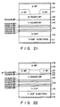
- Fig. 21 shows a semiconductor laser according to one of the embodiments mentioned above.
- An n-type GaP layer 112 as a buffer layer is formed on an n-type GaP substrate 111.
- N-type GaAlN/BP superlattice layers having different average compositions are alternately stacked on the GaP layer 112 to form a buffer layer 113 of a multilayer structure.
- An n-type GaAlN/BP superlattice layer 114 as a first clad layer, an undoped GaAlN/BP superlattice layer 115 as an active layer, and a p-type GaAlN/BP superlattice layer 116 as a second clad layer are sequentially formed on the buffer layer 113.
- n-type BP layer 117 having a striped opening formed at its central portion and serving as a current limit layer is formed on the double-heterojunction structure formed in this manner.
- a p-type BP layer 118 as a contact layer is formed on the resultant structure.
- P- and n-side metal electrodes 110 and 110 are respectively formed on the p-type BP layer 118 and the substrate.
- This semiconductor laser is manufactured by using the MOCVD apparatus of a multi-chamber system shown in Fig. 3 basically under the same conditions of source gases, gas flow rates, doping, and the like as those described in the previous embodiments.
- a typical stacking cycle of the GaAl/BP superlattice layers is 50 ⁇ .
- a ratio or the thickness of a nitride to that of a boride is set as 1 : 1. If this ratio becomes smaller than 1, a band structure is changed from a direct transition type to an indirect transition type, and the light emission efficiency is degraded. If the stacking cycle exceeds 50 ⁇ , electrons and holes locally exist to decrease a conductivity.
- the GaP substrate 111 consists of an Si-doped substrate having a carrier concentration of 1 ⁇ 1017 atoms/cm3; the GaP buffer layer 112, an Si-doped layer having a carrier concentration of 1 ⁇ 1017 atoms/cm3 and a thickness of 1 ⁇ m; the buffer layer 113 of a multilayer structure, a layer obtained by alternately growing n-type GaAlN/BP layers and n-type Ga 0.4 Al 0.6 N/BP layers (Si doping; carrier concentration: 1 ⁇ 1017 atoms/cm3 at a stacking cycle of 500 ⁇ to a thickness of 1 ⁇ m; the n-type first clad layer 114, a Ga 0.4 Al 0.6 N/BP superlattice layer (Si doping; carrier concentration: 1 ⁇ 1017 atoms/cm3 thickness: 1 ⁇ m); the undoped active layer 115, a Ga 0.5 Al 0.5 N/BP superlatti
- a striped SiO2 film having a width of 5 ⁇ m is formed on the p-type clad layer 116 by thermal decomposition and photoetching, and a current blocking layer 117 (Si doping; carrier concentration a 1 ⁇ 1017 atoms/cm3; 1 ⁇ m) consisting of an n-type BP layer is selectively grown.
- the SiO2 film is then removed, and a p-type BP layer 118 (Mg doping; carrier concentration: 1 ⁇ 1017 atoms/cm3 thickness: 1 ⁇ m) as a contact layer is grown on the resultant structure.
- an Au/Zn electrode 119 and an Au/Ge electrode 110 are respectively formed on the p and n sides.
- the wafer obtained in this manner was split along the cleavage plane to obtain a laser having a resonator length of 300 ⁇ m.
- a pulse operation of a pulse width of 100 ⁇ sec at the liquid nitrogen temperature green laser emission was recognized.
- the threshold current density was about 50 kA/cm2.
- No laser oscillation was recognized at room temperature.
- stable light emission for 100 or more hours was recognized. This stable operation seemed to be based on reduction in stress acting on the active layer.
- Fig. 22 shows still another embodiment as a modification of the semiconductor laser of the embodiment described with reference to Fig. 21.
- the n-type BP current blocking layer 117 is formed on the p-type clad layer 116 by the selective growth process.
- the surface of a p-type clad layer 116 is selectively etched in advance to form a striped projection.
- An n-type BP current blocking layer 117 is then formed around the projection.
- Fig. 23 shows still another embodiment as a modification of the semiconductor laser of the embodiment described with reference to Fig. 22.
- each of an n-type clad layer 114, an active layer 115, and the p-type clad layer 116 consists of a GaAlN/BP superlattice layer.
- each of an n-type clad layer 114′, an active layer 115′, and a p-type clad layer 116′ consists of a GaAlBNP mixed crystal layer having a composition equivalent to that of the above superlattice layer.
- a buffer layer having a multilayer structure may be formed by stacking a plurality of Ga x Al y B 1-x-y N z P 1-z mixed crystal layers having different average compositions.
- such a buffer layer may be formed by staking a plurality of GaAlN/BP superlattice layers and Ga x Al y B 1-x-y N z P 1-z mixed crystal layers having different average compositions.
- the buffer layers of multilayer structures described above are also effective for LEDs.
- a composition ratio is changed.
- a superlattice structure is obtained by changing its film thickness ratio
- a mixed crystal is obtained by changing its mixed crystal ratio
- a DH structure can be obtained in the same manner as described above.
- other compositions may be employed.
- x + y becomes smaller than 0.5, the band structure is changed to an indirect transition type. Therefore, the value x + y should not be smaller than 0.5.
- Lattice matching between a BP layer and GaAlN can be improved by adding In (indium) in GaAlN or GaAlBNP.
- Embodiments in which the problem of lattice mismatching between a light-emitting layer portion constituted by a compound semiconductor layer of the present invention and a substrate is solved by selection of substrate materials will be described below.
- a compound semiconductor layer containing boron and nitrogen having large band gaps is grown by the MOCVD method.
- the growth process is preferably performed at a high substrate temperature.
- a GaP substrate described in the above embodiments has a melting point of 1,467°C, the growth process cannot be performed at an excessively high temperature so as to prevent damage to the substrate.
- an SiC substrate having a melting point as high as 2,830°C and a lattice constant smaller than that of a GaP substrate is used, thereby allowing high-temperature growth. Therefore, lattice matching between a substrate and a light-emitting layer portion can be improved.
- Fig. 24 shows a DH structure semiconductor laser according to one of the embodiments mentioned above.
- An n-type BP layer 122 as a buffer layer is formed on an n-type SiC substrate 121.
- An a first clad layer 123 consisting of n-type GaAlN/BP superlattice layer, an active layer 124 consisting of an undoped GaAlN/BP superlattice layer, and a second clad layer 125 consisting of a p-type GaAlN/BP superlattice layer are sequentially formed on the BP layer 122, thus constituting a DH structure.
- a current blocking layer 126 consisting of an n-type BP layer is formed on the second clad layer 125 except for a striped portion formed at its central portion.
- a contact layer 127 consisting of a p-type BP layer is formed on the resultant structure.
- Ohmic electrodes 128 and 129 are respectively formed on the upper and lower surfaces of the element.
- the respective semiconductor layers are grown by using the MOCVD apparatus shown in Fig. 3.
- the growth conditions such as sources gases, gas flow rates, and dopants are the same as those described in the above embodiments.
- the substrate temperature is set at a high temperature, e.g., 1,200 to 1,400°C as compared with the case of a GaP substrate.
- the SiC substrate 121 consists of an Al-doped substrate having a carrier concentration of 1 ⁇ 1017 atoms/cm3; the BP buffer layer 122, an Si-doped layer having a carrier concentration of 1 ⁇ 1017 atoms/cm3 and a thickness of 1 ⁇ m; the first clad layer 123, an n-type Ga 0.4 Al 0.6 N/BP superlattice layer (Si doping: carrier concentration: 1 ⁇ 1017 atoms/cm3; 1 ⁇ m); the active layer 124, an undoped Ga 0.5 Al 0.5 N/BP superlattice layer (0.1 ⁇ m); and the second clad layer 125, a p-type Ga 0.4 Al 0.6 N/BP superlattice layer (Mg doping: carrier concentration: 1 ⁇ 1017 atoms/cm3; 1 ⁇ m).
- a striped SiO2 film mask is formed on the second clad layer 125, and an n-type BP layer (Si doping; carrier concentration: 1 ⁇ 1017 atoms/cm3; 1 ⁇ m) is selectively grown to form a current blocking layer 126.
- the mask is then removed, and a contact layer 127 consisting of a p-type BP layer (Mg doping; carrier concentration: 1 ⁇ 1017 atoms/cm3; 1 ⁇ m) is formed.
- P- and n-side electrodes 128 and 129 are respectively constituted by an Au/Zn film and an Au/Ge film.
- the wafer obtained in this manner was split along the cleavage plane to obtain a laser having a resonator length of 300 ⁇ m.
- a pulse operation of a pulse width of 100 ⁇ sec at the liquid nitrogen temperature green laser emission was recognized.
- the threshold current density was about 50 kA/cm2. No laser oscillation was recognized at room temperature. However, in the LED mode, stable light emission for 100 hours was recognized.
- Fig. 25 shows an arrangement of still another embodiment of a modification of the embodiment described with reference to Fig. 24, in which the light-emitting layer portion is modified.
- the n-type BP current limit layer 126 is selectively grown on the p-type clad layer 125.
- the upper surface of a p-type clad layer 125 is selectively etched in advance to form a striped projection.
- An n-type BP current blocking layer 126 is then formed around the projection.
- Fig. 26 shows still another embodiment of a modification of the semiconductor laser of the embodiment described with reference to Fig. 24.
- each of the n-type clad layer 123, the active layer 124, and the p-type clad layer 125 consists of a GaAlN/BP superlattice layer.
- each of an n-type clad layer 123′, an active layer 124′, and a p-type clad layer 125′ consists of a GaAlBNP mixed crystal layer having the same composition as that of the above-described superlattice layer.
- stable light emission can be realized.
- lattice matching between a BP layer and a GaAlN layer can be improved by adding In (indium) in GaAlN or GaAlGNP.
- an Si substrate can be effectively used for high-temperature growth in place of an SiC substrate. The use of SiC and Si substrates is effective in manufacture of LEDs.
- Each compound semiconductor material of the present invention has a low ionization tendency of BP, a ZB structure, and large band gap properties of GaAlN.
- N is removed, i.e., a self compensating effect occurs.
- p-type doping at a high concentration is difficult to perform. It is found that in order to solve this problem, selective doping of a p-type impurity in only a BP layer having a low ionization tendency is effective when a GaAlN/BP superlattice layer is formed.
- a p-type impurity is doped in the entire GaAlN/BP superlattice layer, in addition to the self compensating effect, a large number of defects are caused, and a high carrier concentration cannot be obtained as a whole.
- a p-type impurity is selectively doped only in the BP layer, the overall structure is free from the influences of the self compensating effect and no defect occurs. As a result, a large number of the doped impurity ions can be effectively activated as a carrier.
- Figs. 27A and 27B illustrate the principle of such a doping method.
- Fig. 27A shows a case wherein a p-type impurity is doped.
- Fig. 27B shows a case wherein an n-type impurity is doped.
- a multilayer structure is basically used, which is obtained by alternately stacking BP and GaAlN layers at a predetermined stacking cycle.
- Mg is doped in only BP layers.
- Fig. 27B Si is doped in only GaAlN layers.
- a GaAlN/BP superlattice layer is formed under the same conditions as those for the formation of each superlattice layer in the above-described embodiments.
- Si is doped as an n-type impurity in the respective GaAlN layers.
- Mg is doped as a p-type impurity in the respective BP layers.
- Si may be simultaneously doped in the GaAlN and BP layers.
- BP has a very large effective mass, it is not suitable for doping of an n-type impurity. It was confirmed that after this selective doping, both p- and n-type superlattice structure semiconductor films each having a carrier concentration on the order of 1018 atoms/cm3 could be obtained.
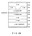
- Fig. 28 shows a semiconductor laser of one of the embodiments above mentioned.
- An n-type GaP buffer layer 132 and an n-type BP buffer layer 133 are sequentially formed on an n-type GaP substrate 131.
- a first clad layer 134 consisting of an n-type GaAlN/BP superlattice layer, an active layer 135 consisting of an undoped GaAlN/BP superlattice layer, and a second clad layer 136 consisting of a p-type GaAlN/BP superlattice layer are sequentially formed on the buffer layer 133, thus constituting a DH structure.
- a current blocking layer 137 consisting of an n-type BP layer is formed on the second clad layer 136 except for a striped portion at its central portion.
- a contact layer 138 consisting of a p-type BP layer is formed on the resultant structure.
- Ohmic electrodes 139 and 130 are respectively formed on the upper and lower surfaces of the element.
- the respective semiconductor layers of this semiconductor laser are grown by using the MOCVD apparatus shown in Fig. 3.
- the growth conditions such as source gases, gas flow rates, and dopants are the same as those in the above-described embodiments.
- Mg is doped only during a growth period of each BP layer.
- Si is doped only during a growth period of each GaAlN layer.
- the GaP substrate 131 consists of an Si-doped substrate having a carrier concentration of 1 ⁇ 1018 atoms/cm3; the n-type GaP buffer layer 132, an Si-doped layer having a carrier concentration of 1 ⁇ 1018 atoms/cm3 and a thickness of 1 ⁇ m; the n-type BP buffer layer 133, an Si-doped layer having a carrier concentration of 1 ⁇ 1018 atoms/cm3 and a thickness of 1 ⁇ m; the first clad layer 134, an n-type Ga 0.4 Al 0.6 N/BP superlattice layer (Si doping; carrier concentration: 1 ⁇ 1018 atoms/cm3; 1 ⁇ m); the active layer 135, an undoped Ga 0.5 Al 0.5 N/BP superlattice layer (0.1 ⁇ m); and the second clad layer 136, a p-type Ga 0.4 Al 0.6 N/BP superlattice layer (Si doping; carrier concentration: 1
- a striped SiO2 film mask is formed on the second clad layer 136, and an n-type BP layer (Si doping; carrier concentration: 1 ⁇ 1018 atoms/cm3; 1 ⁇ m) is selectively grown to form a current blocking layer 137. Thereafter, the mask is removed, and a contact layer 138 consisting of a p-type BP layer (Mg doping; carrier concentration: 1 ⁇ 1018 atoms/cm3; 1 ⁇ m) is formed on the resultant structure.
- a p-side electrode 139 consists of an Au/Zn film; and an n-side electrode 130, an Au/Ge film.
- the wafer obtained in this manner was split along the cleavage plane to obtain a laser having a resonator length of 300 ⁇ m.
- a pulse operation of a pulse width of 100 ⁇ sec at the liquid nitrogen temperature green laser emission was recognized.
- the threshold current density was about 50 kA/cm2. No laser oscillation was recognized at room temperature. However, in the LED mode, stable light emission for 100 hours was recognized.
- Fig. 29 shows still another embodiment of a modification of the semiconductor laser of the embodiment described with reference to Fig. 28.
- the layer 136 is selectively etched to form a striped projection at its central portion, and a current blocking layer 137 consisting of an n-type BP layer is formed around the projection.
- the projection of the second clad layer 136 serves as an optical waveguide because of a difference in refractive index between the projection and the current blocking layer 137. As a result, current limiting and optical confinement can be realized in the manner of self matching.
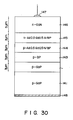
- Fig. 30 shows an embodiment in which selective doping of impurities in superlattice layers.
- a p-type GaP buffer layer 142 and a p-type BP buffer layer 143 are sequentially formed on a p-type GaP substrate 141.
- a p-n junction consisting of a p-type Ga 0.5 Al 0.5 N/BP superlattice layer 144 and an n-type Ga 0.5 Al 0.5 B/BP superlattice layer 145 is formed on the BP buffer layer 143.
- An n-type GaN contact layer 146 is formed on the resultant structure.
- Ohmic electrodes 147 and 148 are respectively formed on the upper and lower surfaces of the element.
- This LED can be formed by using the MOCVD apparatus shown in Fig. 3 substantially under the same conditions as those in the above-described embodiments.
- the GaP substrate 141 consists of a Zn-doped substrate having a carrier concentration of 2 ⁇ 1017 atoms/cm3.
- Each of the p-type GaP buffer layer 142 and the p-type BP buffer layer 143 has a carrier concentration of 2 ⁇ 1017 atoms/cm3 and a thickness of 3 ⁇ m.
- the p-type Ga 0.5 Al 0.5 N/BP superlattice layer 144 has a multilayer structure (band gap: 3.0 eV) formed at a stacking cycle of 13 ⁇ /7 ⁇ and having a carrier concentration of 1 ⁇ 1017 atoms/cm3 and a thickness of 3 ⁇ m.
- the n-type Ga 0.5 Al 0.5 N/BP superlattice layer 145 has a multilayer structure (band gap: 2.7 eV) formed at a stacking cycle of 10 ⁇ /10 ⁇ and having a carrier concentration of 2 ⁇ 1016 atoms/cm3 and a thickness of 3 ⁇ m. Most of the n-type GaN contact layer 146 is formed into a WZ structure. The layer 146 is doped with Si and has a carrier concentration of 1 ⁇ 1017 atoms/cm3 and a thickness of 5 ⁇ m. When the p-type Ga 0.5 Al 0.5 N/BP superlattice layer 144 is formed, Mg doping is performed only duing a growth period of each BP layer. When the n-type Ga 0.5 Al 0.5 N/BP superlattice layer 145 is formed, Si doping is performed only during a growth period of each GaAlN layer.
- Fig. 31 shows a state wherein an LED chip 151 obtained in this manner is embedded in a resin case 152 serving also as a lens.
- One terminal of the element is connected to one of external leads 154 through an internal lead 153.
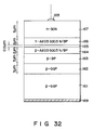
- Fig. 32 shows an embodiment in which the selective doping method for superlattice layers is applied to an LED having a DH structure.
- a p-type GaP buffer layer 162 and a p-type BP buffer layer 163 are sequentially formed on a p-type GaP substrate 161.
- a p-type Ga 0.5 Al 0.5 N/BP superlattice layer 164, an undoped Ga 0.5 Al 0.5 N/BP layer 165, and an n-type Ga 0.5 Al 0.5 N/BP layer 166 are sequentially stacked on the buffer layer 163.
- An n-type contact layer 167 is formed on the resultant structure.
- Ohmic electrodes 168 and 169 are formed on the upper and lower surfaces of the element wafer.
- This LED can also be formed by the MOCVD apparatus shown in Fig. 3 substantially under the same conditions as those in the above-described embodiments.
- the GaP substrate 161 consists of a Zn-doped substrate having a carrier concentration of 2 ⁇ 1017 atoms/cm3.
- Each of the p-type Gap buffer layer 162 and the p-type BP buffer layer 163 has a carrier concentration of 2 ⁇ 1017 atoms/cm3 and a thickness of 3 ⁇ m.
- the p-type Ga 0.5 Al 0.5 N/BP superlattice layer 164 has a multilayer structure formed at a stacking cycle of 13 ⁇ /7 ⁇ and having a carrier concentration of 1 ⁇ 1017 atoms/cm3 and a thickness of 2 ⁇ m.
- the undoped Ga 0.5 Al 0.5 N/BP superlattice layer 165 has a multilayer structure formed at a stacking cycle of 10 ⁇ /10 ⁇ and having a carrier concentration of 2 ⁇ 1016 atoms/cm3 and a thickness of 0.5 ⁇ m.
- the n-type Ga 0.5 Al 0.5 N/BP superlattice layer 166 has a multilayer structure formed at a stacking cycle of 13 ⁇ /7 ⁇ and having a carrier concentration of 2 ⁇ 1016 atoms/cm3 and a thickness of 2 ⁇ m. Most of the n-type GaN contact layer 167 is formed into a WZ structure.
- the layer 167 is doped with Si and has a carrier concentration of 1 ⁇ 1017 atoms/cm3 and a thickness of 5 ⁇ m.
- Mg doping is performed only duing a growth period of each BP layer.
- Si doping is performed only during a growth period of each GaAlN layer.
- element formation does not always require a low-resistance p-n junction but sometimes require only a large band gap. Therefore, if ZB type materials which allow easy formation of a low-resistance p-n junction is combined with WZ type materials which can increase a growth rate and allows easy growth of layers under a wide range of growth conditions, the degree of freedom of element design and the margin of manufacture can be increased. As a result, the performance of an element and the manufacturing yield can greatly be increased.
- a ZB layer is grown in a relatively narrow range of growth conditions. Especially if the grow rate of a layer having a composition of a large band gap is increased, most of the resultant layer acquires a WZ type structure. In this case, a low-resistance p-type layer cannot be realized. However, large band gaps of GaN and AlN of a direct transition type and low ionization tendency and stability of BP can be utilized. That is, p-n junctions and heterojunctions can be formed in the same manner as in the case wherein ZB type materials are used except that a p-type layer has a relatively high resistance. Therefore, if formation of a thick layer is required while a p-type layer need not have a high carrier concentration, it is advantageous to form a whole element by using WZ type materials in terms of each manufacture.
- a compound semiconductor material which has a large band gap, allows easy p-n junction control, and is excellent in crystallinity can be obtained.
- a short wavelength light-emitting diode or laser, which has not been available, can be obtained by using this material.
Landscapes
- Physics & Mathematics (AREA)
- Optics & Photonics (AREA)
- Chemical & Material Sciences (AREA)
- Engineering & Computer Science (AREA)
- Nanotechnology (AREA)
- Condensed Matter Physics & Semiconductors (AREA)
- General Physics & Mathematics (AREA)
- Electromagnetism (AREA)
- Life Sciences & Earth Sciences (AREA)
- Biophysics (AREA)
- Crystallography & Structural Chemistry (AREA)
- Led Devices (AREA)
Applications Claiming Priority (4)
| Application Number | Priority Date | Filing Date | Title |
|---|---|---|---|
| JP622289 | 1989-01-13 | ||
| JP6222/89 | 1989-01-13 | ||
| JP110501/89 | 1989-04-28 | ||
| JP1110501A JP2809690B2 (ja) | 1989-01-13 | 1989-04-28 | 化合物半導体材料とこれを用いた半導体素子およびその製造方法 |
Publications (3)
| Publication Number | Publication Date |
|---|---|
| EP0377940A2 true EP0377940A2 (de) | 1990-07-18 |
| EP0377940A3 EP0377940A3 (de) | 1991-05-29 |
| EP0377940B1 EP0377940B1 (de) | 1994-11-17 |
Family
ID=26340303
Family Applications (1)
| Application Number | Title | Priority Date | Filing Date |
|---|---|---|---|
| EP89310004A Expired - Lifetime EP0377940B1 (de) | 1989-01-13 | 1989-09-29 | Verbindungshalbleiter, denselben anwendendes Halbleiter-Bauelement und Herstellungsverfahren des Halbleiter-Bauelementes |
Country Status (3)
| Country | Link |
|---|---|
| US (1) | US5076860A (de) |
| EP (1) | EP0377940B1 (de) |
| DE (1) | DE68919408T2 (de) |
Cited By (10)
| Publication number | Priority date | Publication date | Assignee | Title |
|---|---|---|---|---|
| EP0551721A3 (de) * | 1991-12-18 | 1994-04-20 | Amano Hiroshi | |
| WO1996030945A3 (en) * | 1995-03-29 | 1996-12-12 | Univ North Carolina State | Integrated heterostructures of group iii-v nitride semiconductor materials and methods for fabricating the same |
| US5670798A (en) * | 1995-03-29 | 1997-09-23 | North Carolina State University | Integrated heterostructures of Group III-V nitride semiconductor materials including epitaxial ohmic contact non-nitride buffer layer and methods of fabricating same |
| GB2343294A (en) * | 1998-10-31 | 2000-05-03 | Sharp Kk | Lattice-matched semiconductor devices |
| EP1003227A3 (de) * | 1998-11-06 | 2000-08-30 | Matsushita Electronics Corporation | Halbleitervorrichtung |
| EP0810674A3 (de) * | 1996-05-31 | 2001-10-24 | Sumitomo Electric Industries, Ltd. | Lichtemittierende Vorrichtung, Wafer für lichtemittierende Vorrichtung und Herstellungsverfahren |
| WO2003023095A1 (fr) * | 2001-09-06 | 2003-03-20 | Toshiba Ceramics Co., Ltd. | Plaquette de semi-conducteur et production de cette plaquette |
| WO2002097861A3 (en) * | 2001-05-28 | 2003-07-24 | Showa Denko Kk | Semiconductor device, semiconductor layer and production method thereof |
| WO2003054929A3 (de) * | 2001-12-21 | 2004-04-08 | Aixtron Ag | Verfahren zum abscheiden von iii-v-halbleiterschichten auf einem nicht-iii-v-substrat |
| CN112758902A (zh) * | 2021-01-06 | 2021-05-07 | 西南科技大学 | 用于高效析氧反应的优化电子构型Co4N纳米片的制备方法 |
Families Citing this family (46)
| Publication number | Priority date | Publication date | Assignee | Title |
|---|---|---|---|---|
| US6362017B1 (en) | 1990-02-28 | 2002-03-26 | Toyoda Gosei Co., Ltd. | Light-emitting semiconductor device using gallium nitride group compound |
| EP0444630B1 (de) | 1990-02-28 | 1997-05-21 | Toyoda Gosei Co., Ltd. | Lichtemittierende Halbleitervorrichtung mit Gallium-Nitrid-Verbindung |
| US6830992B1 (en) * | 1990-02-28 | 2004-12-14 | Toyoda Gosei Co., Ltd. | Method for manufacturing a gallium nitride group compound semiconductor |
| US5173751A (en) * | 1991-01-21 | 1992-12-22 | Pioneer Electronic Corporation | Semiconductor light emitting device |
| DE69229265T2 (de) * | 1991-03-18 | 1999-09-23 | Trustees Of Boston University, Boston | Verfahren zur herstellung und dotierung hochisolierender dünner schichten aus monokristallinem galliumnitrid |
| US5633192A (en) * | 1991-03-18 | 1997-05-27 | Boston University | Method for epitaxially growing gallium nitride layers |
| US6953703B2 (en) * | 1991-03-18 | 2005-10-11 | The Trustees Of Boston University | Method of making a semiconductor device with exposure of sapphire substrate to activated nitrogen |
| US5192987A (en) * | 1991-05-17 | 1993-03-09 | Apa Optics, Inc. | High electron mobility transistor with GaN/Alx Ga1-x N heterojunctions |
| US5578839A (en) * | 1992-11-20 | 1996-11-26 | Nichia Chemical Industries, Ltd. | Light-emitting gallium nitride-based compound semiconductor device |
| DE69431333T2 (de) * | 1993-10-08 | 2003-07-31 | Mitsubishi Cable Industries, Ltd. | GaN-Einkristall |
| US5689123A (en) | 1994-04-07 | 1997-11-18 | Sdl, Inc. | III-V aresenide-nitride semiconductor materials and devices |
| US6130147A (en) * | 1994-04-07 | 2000-10-10 | Sdl, Inc. | Methods for forming group III-V arsenide-nitride semiconductor materials |
| US5814533A (en) * | 1994-08-09 | 1998-09-29 | Rohm Co., Ltd. | Semiconductor light emitting element and manufacturing method therefor |
| US5661074A (en) * | 1995-02-03 | 1997-08-26 | Advanced Technology Materials, Inc. | High brightness electroluminescent device emitting in the green to ultraviolet spectrum and method of making the same |
| US5677538A (en) * | 1995-07-07 | 1997-10-14 | Trustees Of Boston University | Photodetectors using III-V nitrides |
| JP3564811B2 (ja) * | 1995-07-24 | 2004-09-15 | 豊田合成株式会社 | 3族窒化物半導体発光素子 |
| JP3060973B2 (ja) * | 1996-12-24 | 2000-07-10 | 日本電気株式会社 | 選択成長法を用いた窒化ガリウム系半導体レーザの製造方法及び窒化ガリウム系半導体レーザ |
| US5838707A (en) * | 1996-12-27 | 1998-11-17 | Motorola, Inc. | Ultraviolet/visible light emitting vertical cavity surface emitting laser and method of fabrication |
| US6599133B2 (en) * | 1997-11-18 | 2003-07-29 | Technologies And Devices International, Inc. | Method for growing III-V compound semiconductor structures with an integral non-continuous quantum dot layer utilizing HVPE techniques |
| US6316098B1 (en) | 1998-03-27 | 2001-11-13 | Yissum Research Development Company Of The Hebrew University Of Jerusalem | Molecular layer epitaxy method and compositions |
| US6783849B2 (en) | 1998-03-27 | 2004-08-31 | Yissum Research Development Company Of The Hebrew University Of Jerusalem | Molecular layer epitaxy method and compositions |
| US6984851B2 (en) * | 2000-06-21 | 2006-01-10 | Showa Denko Kabushiki Kaisha | Group-III nitride semiconductor light-emitting diode, light-emitting diode lamp, light source, electrode for group-III nitride semiconductor light-emitting diode, and method for producing the electrode |
| US6420732B1 (en) | 2000-06-26 | 2002-07-16 | Luxnet Corporation | Light emitting diode of improved current blocking and light extraction structure |
| US6706119B2 (en) * | 2001-03-30 | 2004-03-16 | Technologies And Devices International, Inc. | Apparatus for epitaxially growing semiconductor device structures with submicron group III nitride layer utilizing HVPE |
| US7501023B2 (en) * | 2001-07-06 | 2009-03-10 | Technologies And Devices, International, Inc. | Method and apparatus for fabricating crack-free Group III nitride semiconductor materials |
| US20070032046A1 (en) * | 2001-07-06 | 2007-02-08 | Dmitriev Vladimir A | Method for simultaneously producing multiple wafers during a single epitaxial growth run and semiconductor structure grown thereby |
| US20060011135A1 (en) * | 2001-07-06 | 2006-01-19 | Dmitriev Vladimir A | HVPE apparatus for simultaneously producing multiple wafers during a single epitaxial growth run |
| US6936357B2 (en) * | 2001-07-06 | 2005-08-30 | Technologies And Devices International, Inc. | Bulk GaN and ALGaN single crystals |
| US6613143B1 (en) * | 2001-07-06 | 2003-09-02 | Technologies And Devices International, Inc. | Method for fabricating bulk GaN single crystals |
| DE10234694A1 (de) * | 2002-07-30 | 2004-02-12 | Infineon Technologies Ag | Verfahren zum Oxidieren einer Schicht und zugehörige Aufnamevorrichtung für ein Substrat |
| US7034330B2 (en) * | 2002-10-22 | 2006-04-25 | Showa Denko Kabushiki Kaisha | Group-III nitride semiconductor device, production method thereof and light-emitting diode |
| US7786550B2 (en) * | 2003-03-06 | 2010-08-31 | Panasonic Corporation | P-type semiconductor and semiconductor hetero material and manufacturing methods thereof |
| US20050115492A1 (en) * | 2003-11-28 | 2005-06-02 | Chia-Cheng Liu | Method and apparatus of the chemical metal organic vapor epitaxy for the multi-chamber epitaxy layer deposition |
| WO2005096355A1 (en) * | 2004-03-30 | 2005-10-13 | Showa Denko K.K | Compound semiconductor device, production method of compound semiconductor device and diode |
| TWI258183B (en) * | 2004-04-28 | 2006-07-11 | Showa Denko Kk | Compound semiconductor light-emitting device |
| TWI296160B (en) * | 2004-05-06 | 2008-04-21 | Showa Denko Kk | Pn junction-type compound semiconductor light emitting diode |
| JP4661088B2 (ja) * | 2004-06-01 | 2011-03-30 | 住友化学株式会社 | pn接合を有する化合物半導体基板の製造方法 |
| US20070006801A1 (en) * | 2005-07-09 | 2007-01-11 | Stringfellow Gerald B | Use of surfactants to control unintentional dopant in semiconductors |
| US9416464B1 (en) | 2006-10-11 | 2016-08-16 | Ostendo Technologies, Inc. | Apparatus and methods for controlling gas flows in a HVPE reactor |
| KR101172143B1 (ko) * | 2009-08-10 | 2012-08-07 | 엘지이노텍 주식회사 | 백색 발광다이오드 소자용 시온계 산화질화물 형광체, 그의 제조방법 및 그를 이용한 백색 led 소자 |
| WO2011028033A2 (ko) * | 2009-09-02 | 2011-03-10 | 엘지이노텍주식회사 | 형광체, 형광체 제조방법 및 백색 발광 소자 |
| KR101163902B1 (ko) | 2010-08-10 | 2012-07-09 | 엘지이노텍 주식회사 | 발광 소자 |
| US11393683B2 (en) * | 2009-10-14 | 2022-07-19 | Utica Leaseco, Llc | Methods for high growth rate deposition for forming different cells on a wafer |
| US9834860B2 (en) * | 2009-10-14 | 2017-12-05 | Alta Devices, Inc. | Method of high growth rate deposition for group III/V materials |
| JP5996846B2 (ja) * | 2011-06-30 | 2016-09-21 | シャープ株式会社 | 窒化物半導体発光素子およびその製造方法 |
| CN110494987B (zh) * | 2017-04-24 | 2022-03-01 | 苏州晶湛半导体有限公司 | 一种半导体结构和制备半导体结构的方法 |
Family Cites Families (8)
| Publication number | Priority date | Publication date | Assignee | Title |
|---|---|---|---|---|
| DE2214224C3 (de) * | 1972-03-23 | 1978-05-03 | Siemens Ag, 1000 Berlin Und 8000 Muenchen | Verfahren zur Bildung von pn-Übergängen in III-V-Halbleiter-Einkristallen |
| US4213781A (en) * | 1978-11-20 | 1980-07-22 | Westinghouse Electric Corp. | Deposition of solid semiconductor compositions and novel semiconductor materials |
| JPS56116673A (en) * | 1980-02-19 | 1981-09-12 | Sharp Corp | Amorphous thin film solar cell |
| JPS56145199A (en) * | 1980-04-04 | 1981-11-11 | Showa Denko Kk | Synthesis of cubic boron nitride |
| US4697202A (en) * | 1984-02-02 | 1987-09-29 | Sri International | Integrated circuit having dislocation free substrate |
| JPS62243144A (ja) * | 1986-04-15 | 1987-10-23 | Dainippon Printing Co Ltd | 光学的記録媒体および光学的記録方法 |
| GB2206257B (en) * | 1987-05-26 | 1991-08-14 | Clarion Co Ltd | Surface acoustic wave device |
| NL8701497A (nl) * | 1987-06-26 | 1989-01-16 | Philips Nv | Halfgeleiderinrichting voor het opwekken van electromagnetische straling. |
-
1989
- 1989-09-29 DE DE68919408T patent/DE68919408T2/de not_active Expired - Fee Related
- 1989-09-29 EP EP89310004A patent/EP0377940B1/de not_active Expired - Lifetime
- 1989-09-29 US US07/414,520 patent/US5076860A/en not_active Expired - Lifetime
Cited By (18)
| Publication number | Priority date | Publication date | Assignee | Title |
|---|---|---|---|---|
| EP0551721A3 (de) * | 1991-12-18 | 1994-04-20 | Amano Hiroshi | |
| WO1996030945A3 (en) * | 1995-03-29 | 1996-12-12 | Univ North Carolina State | Integrated heterostructures of group iii-v nitride semiconductor materials and methods for fabricating the same |
| US5670798A (en) * | 1995-03-29 | 1997-09-23 | North Carolina State University | Integrated heterostructures of Group III-V nitride semiconductor materials including epitaxial ohmic contact non-nitride buffer layer and methods of fabricating same |
| US5679965A (en) * | 1995-03-29 | 1997-10-21 | North Carolina State University | Integrated heterostructures of Group III-V nitride semiconductor materials including epitaxial ohmic contact, non-nitride buffer layer and methods of fabricating same |
| US6046464A (en) * | 1995-03-29 | 2000-04-04 | North Carolina State University | Integrated heterostructures of group III-V nitride semiconductor materials including epitaxial ohmic contact comprising multiple quantum well |
| EP0810674A3 (de) * | 1996-05-31 | 2001-10-24 | Sumitomo Electric Industries, Ltd. | Lichtemittierende Vorrichtung, Wafer für lichtemittierende Vorrichtung und Herstellungsverfahren |
| EP1777756A1 (de) * | 1996-05-31 | 2007-04-25 | Sumitomo Electric Industries, Ltd. | Lichtemittierende Halbleitervorrichtung, Wafer für eine lichtemittierende Halbleitervorrichtung und Herstellungsverfahren dafür |
| GB2343294A (en) * | 1998-10-31 | 2000-05-03 | Sharp Kk | Lattice-matched semiconductor devices |
| EP1003227A3 (de) * | 1998-11-06 | 2000-08-30 | Matsushita Electronics Corporation | Halbleitervorrichtung |
| US6150674A (en) * | 1998-11-06 | 2000-11-21 | Matsushita Electronics Corporation | Semiconductor device having Alx Ga1-x N (0<x<1) substrate |
| WO2002097861A3 (en) * | 2001-05-28 | 2003-07-24 | Showa Denko Kk | Semiconductor device, semiconductor layer and production method thereof |
| US7315050B2 (en) | 2001-05-28 | 2008-01-01 | Showa Denko K.K. | Semiconductor device, semiconductor layer and production method thereof |
| US7622398B2 (en) | 2001-05-28 | 2009-11-24 | Showa Denko K.K. | Semiconductor device, semiconductor layer and production method thereof |
| WO2003023095A1 (fr) * | 2001-09-06 | 2003-03-20 | Toshiba Ceramics Co., Ltd. | Plaquette de semi-conducteur et production de cette plaquette |
| US6936490B2 (en) | 2001-09-06 | 2005-08-30 | Toshiba Ceramics Co, Ltd. | Semiconductor wafer and its manufacturing method |
| WO2003054929A3 (de) * | 2001-12-21 | 2004-04-08 | Aixtron Ag | Verfahren zum abscheiden von iii-v-halbleiterschichten auf einem nicht-iii-v-substrat |
| CN112758902A (zh) * | 2021-01-06 | 2021-05-07 | 西南科技大学 | 用于高效析氧反应的优化电子构型Co4N纳米片的制备方法 |
| CN112758902B (zh) * | 2021-01-06 | 2022-01-28 | 西南科技大学 | 用于高效析氧反应的优化电子构型Co4N纳米片的制备方法 |
Also Published As
| Publication number | Publication date |
|---|---|
| DE68919408D1 (de) | 1994-12-22 |
| EP0377940A3 (de) | 1991-05-29 |
| EP0377940B1 (de) | 1994-11-17 |
| US5076860A (en) | 1991-12-31 |
| DE68919408T2 (de) | 1995-04-20 |
Similar Documents
| Publication | Publication Date | Title |
|---|---|---|
| EP0377940B1 (de) | Verbindungshalbleiter, denselben anwendendes Halbleiter-Bauelement und Herstellungsverfahren des Halbleiter-Bauelementes | |
| JP2809690B2 (ja) | 化合物半導体材料とこれを用いた半導体素子およびその製造方法 | |
| US5005057A (en) | Semiconductor light-emitting diode and method of manufacturing the same | |
| EP0395392B1 (de) | Halbleiterlaser mit fünfelementigem Verbindungshalbleiter | |
| EP0844675B1 (de) | Lichtemittierende Vorrichtung auf Basis einer Galliumnitrid-Halbleiterverbindung | |
| KR100993408B1 (ko) | 발광 소자 및 그 제조 방법 | |
| US6020602A (en) | GaN based optoelectronic device and method for manufacturing the same | |
| US7888669B2 (en) | Nitride/zinc oxide based light-emitting diodes | |
| EP0551721A2 (de) | Halbleiteranordnung auf Basis von Gallium-Nitrid und Verfahren zur Herstellung | |
| JP3064891B2 (ja) | 3−5族化合物半導体とその製造方法および発光素子 | |
| TWI898778B (zh) | 光半導體元件及其製造方法 | |
| US7525128B2 (en) | Zinc-oxide-based double-heterostructure light-emitting diode | |
| JPH10247761A (ja) | 青色半導体発光素子 | |
| JP3152902B2 (ja) | 青色半導体発光素子 | |
| KR100802451B1 (ko) | 인화 붕소계 반도체 발광 소자 | |
| JPH10247760A (ja) | 青色半導体発光素子 | |
| JPH10242514A (ja) | 青色半導体発光素子 | |
| JP3646706B2 (ja) | リン化硼素系半導体発光ダイオードおよびその製造方法 | |
| JPH08222764A (ja) | 発光ダイオード | |
| JP4156873B2 (ja) | エピタキシャルウエハの製造方法 | |
| JPH10242515A (ja) | 青色半導体発光素子 | |
| JP2003229601A (ja) | リン化硼素系半導体素子、その製造方法、および発光ダイオード | |
| JPH08162481A (ja) | 結晶成長方法 |
Legal Events
| Date | Code | Title | Description |
|---|---|---|---|
| PUAI | Public reference made under article 153(3) epc to a published international application that has entered the european phase |
Free format text: ORIGINAL CODE: 0009012 |
|
| 17P | Request for examination filed |
Effective date: 19891025 |
|
| AK | Designated contracting states |
Kind code of ref document: A2 Designated state(s): DE FR GB |
|
| RHK1 | Main classification (correction) |
Ipc: H01L 29/201 |
|
| PUAL | Search report despatched |
Free format text: ORIGINAL CODE: 0009013 |
|
| AK | Designated contracting states |
Kind code of ref document: A3 Designated state(s): DE FR GB |
|
| 17Q | First examination report despatched |
Effective date: 19930329 |
|
| GRAA | (expected) grant |
Free format text: ORIGINAL CODE: 0009210 |
|
| AK | Designated contracting states |
Kind code of ref document: B1 Designated state(s): DE FR GB |
|
| REF | Corresponds to: |
Ref document number: 68919408 Country of ref document: DE Date of ref document: 19941222 |
|
| ET | Fr: translation filed | ||
| PLBE | No opposition filed within time limit |
Free format text: ORIGINAL CODE: 0009261 |
|
| STAA | Information on the status of an ep patent application or granted ep patent |
Free format text: STATUS: NO OPPOSITION FILED WITHIN TIME LIMIT |
|
| PG25 | Lapsed in a contracting state [announced via postgrant information from national office to epo] |
Ref country code: GB Effective date: 19950929 |
|
| 26N | No opposition filed | ||
| GBPC | Gb: european patent ceased through non-payment of renewal fee |
Effective date: 19950929 |
|
| REG | Reference to a national code |
Ref country code: FR Ref legal event code: D6 |
|
| PGFP | Annual fee paid to national office [announced via postgrant information from national office to epo] |
Ref country code: FR Payment date: 20020910 Year of fee payment: 14 |
|
| PGFP | Annual fee paid to national office [announced via postgrant information from national office to epo] |
Ref country code: DE Payment date: 20021002 Year of fee payment: 14 |
|
| PG25 | Lapsed in a contracting state [announced via postgrant information from national office to epo] |
Ref country code: DE Free format text: LAPSE BECAUSE OF NON-PAYMENT OF DUE FEES Effective date: 20040401 |
|
| PG25 | Lapsed in a contracting state [announced via postgrant information from national office to epo] |
Ref country code: FR Free format text: LAPSE BECAUSE OF NON-PAYMENT OF DUE FEES Effective date: 20040528 |
|
| REG | Reference to a national code |
Ref country code: FR Ref legal event code: ST |