EP0378332A2 - Halbleiterspeichergerät mit Redundanzschaltungen - Google Patents
Halbleiterspeichergerät mit Redundanzschaltungen Download PDFInfo
- Publication number
- EP0378332A2 EP0378332A2 EP90300175A EP90300175A EP0378332A2 EP 0378332 A2 EP0378332 A2 EP 0378332A2 EP 90300175 A EP90300175 A EP 90300175A EP 90300175 A EP90300175 A EP 90300175A EP 0378332 A2 EP0378332 A2 EP 0378332A2
- Authority
- EP
- European Patent Office
- Prior art keywords
- column
- columns
- data lines
- data line
- spare
- Prior art date
- Legal status (The legal status is an assumption and is not a legal conclusion. Google has not performed a legal analysis and makes no representation as to the accuracy of the status listed.)
- Granted
Links
- 239000004065 semiconductor Substances 0.000 title claims description 21
- 230000015654 memory Effects 0.000 claims abstract description 62
- 238000012546 transfer Methods 0.000 claims description 22
- 238000007664 blowing Methods 0.000 claims description 4
- 230000002950 deficient Effects 0.000 abstract description 24
- 230000007547 defect Effects 0.000 abstract description 18
- 230000008439 repair process Effects 0.000 abstract description 6
- 230000008520 organization Effects 0.000 description 10
- 238000010586 diagram Methods 0.000 description 5
- 238000010276 construction Methods 0.000 description 3
- 238000007796 conventional method Methods 0.000 description 3
- 238000004519 manufacturing process Methods 0.000 description 3
- 238000007689 inspection Methods 0.000 description 2
- 230000010354 integration Effects 0.000 description 2
- 239000011159 matrix material Substances 0.000 description 2
- 230000009467 reduction Effects 0.000 description 2
- 230000003213 activating effect Effects 0.000 description 1
- 230000008901 benefit Effects 0.000 description 1
- 230000000295 complement effect Effects 0.000 description 1
- 238000005520 cutting process Methods 0.000 description 1
- 238000013461 design Methods 0.000 description 1
- 230000000694 effects Effects 0.000 description 1
- 238000012545 processing Methods 0.000 description 1
- 230000005855 radiation Effects 0.000 description 1
- 230000007480 spreading Effects 0.000 description 1
- 238000003892 spreading Methods 0.000 description 1
- 230000003068 static effect Effects 0.000 description 1
Images




Classifications
-
- G—PHYSICS
- G11—INFORMATION STORAGE
- G11C—STATIC STORES
- G11C29/00—Checking stores for correct operation ; Subsequent repair; Testing stores during standby or offline operation
- G11C29/70—Masking faults in memories by using spares or by reconfiguring
- G11C29/78—Masking faults in memories by using spares or by reconfiguring using programmable devices
- G11C29/80—Masking faults in memories by using spares or by reconfiguring using programmable devices with improved layout
- G11C29/808—Masking faults in memories by using spares or by reconfiguring using programmable devices with improved layout using a flexible replacement scheme
Definitions
- the present invention relates to a semiconductor memory device comprising a memory cell array having plural memory cells arranged in matrix, and plural I/O data lines, and more particularly to its redundancy circuits.
- redundancy circuits are generally provided in order to lower the manufacturing cost. They are intended to dispose spare memory cells aside from the regular memory cells on the memory chip, and if defect is found in part of the regular cells in wafer inspection, replace them with the spare memory cells, thereby rescuing the defective chips of small bits.
- a spare row or a spare column for replacing the row or column containing defective memory cells, or both of them are provided, and when the row address or column address of the row or column containing defective memory cells is selected, the row or column in the regular memory cell array is not selected, but the spare row or spare column is selected.
- the ⁇ 4 bit organization is common in the DRAM, and the ⁇ 8 bit organization in the static random access memory (SRAM), but henceforth it is expected that memories of ⁇ 16 bit organization, ⁇ 32 bit organization and even ⁇ 64 bit organization will be required.
- Figs. 5 and 6 Examples of application of conventional redundancy circuits in such multi-bit memory device are shown in Figs. 5 and 6.
- the number of column addresses is four in ⁇ 4 bit organization.
- the column lines and I/O data, lines are actually composed of a pair of two lines including the line for complementary data, but they are expressed by one line in these examples.
- bit lines column possessing common column addresses are disposed adjacently.
- the bit lines B1, B2, ..., B16 are regular bit lines.
- D1, D2, D3, D4 are I/O data lines corresponding to each one of input, output data 4 bits.
- Transistors T1, T2, ..., T16 electrically connect the regular bit lines B1 to B16 to I/O data lines D1 to D4, according to the column selection signal lines C1, C2, C3, C4 decoded and activated by a regular column decoder 10.
- B17, B18, B19, B20 are spare bit lines, and if there is any defect in the memory cell on any of the regular bit lines B1 to B16 electrically connectable to the I/O data lines D1 to D4, such defective bit lines are replaced by spare bit lines B17 to B20.
- a redundancy column decoder 20 activates the redundancy column selection signal line C5 when the column address including the defective memory cell is selected. As a result, the transistors T17, T18, T19, T20 are made to conduct, and the spare bit lines B17 to B20 are electrically connected to the I/O data lines D1 to D4. At the same time, the column selection signal line to be activated by this row address if there is no defect in the regular memory cells remains inactive.
- the column address for activating the redundancy column selection signal line is set up by cutting off part of the fuse preliminarily formed on the chip by laser after discovering the defective memory cell in wafer inspection.
- Fig. 6 is an example in which the bit lines electrically connected to the same I/O data line are disposed adjacently.
- the regular bit lines B1, B2 ..., B16 are disposed as being divided into four blocks for every corresponding I/O data line.
- the column decoders 10, 11, 12, 13 are disposed in each block, and according to the column address, one from each block of column selection signal lines C01, C02, C03, C04, C11, C12, C13, C14, C21, C22, C23, C24, C31, C32, C33, C34, for example, the column selection signal lines C01, C11, C21, C31 are activated.
- Spare bit lines B17, B18, B19, B20, and redundancy column decoders 20, 21, 22, 23 are also disposed by one in each blook.
- all of redundancy column selection signal lines C05, C15, C25, C35 are activated, and the transistors T17, T18, T19, T20 are made to conduct, and the spare bit lines B17, B18, B19, B20 are electrically connected to the I/O data lines D1, D2, D3, D4 respectively.
- the column selection signal line to be activated by the column address if there is no defect in the regular memory cells remains inactive.
- the status of occurrence of defective memory cell is not completely random, but often adjacent memory cells become defective at the same time, or the adjacent bit lines are short-circuited to make two columns defective simultaneously.
- the column redundancy circuit shown in Fig. 6 one bit line is replaced by the redundancy bit lint in each block, and therefore if the adjacent upper and lower memory cells become defective at the same time, or the adjacent bit lines are short-circuited to be defective, it is impossible to rescue them.
- it is disadvantageous that the efficiency of repair with the redundancy circuit is not raised so high.
- the invention is intended to compose a redundancy circuit so as to replace the bit lines to be electrically connected to a specific I/O data line with the spare bit lines, instead of replacing the bit lines having a specific column address with spare bit lines, while maintaining the same circuit and composition as in Fig. 6 for the regular memory cells because it is advantageous in layout.
- all bit lines sharing the I/O data line with such column are isolated from the I/O data line regardless of the column address, and, instead, of group of spare bit lines being disposed corresponding to each column address and selected according to the column address is electrically connected to the same I/O data line.
- the bit lines are disposed by dividing into each corresponding I/O data line, and if there are defects over two or more adjacent columns, as far as they are within the block of same I/O data line, all defective memory cells may be replaced by the memory cells of the spare column. Therefore, while minimizing the increase of chip area and reduction of operating speed due to multi-bit organization, a redundancy circuit high in the efficiency of repair may be realized.
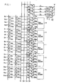
- FIG. 1 A first embodiment of multi-bit organized semiconductor memory of the invention is shown in Fig. 1.
- Fig. 1 same as in Fig. 5, Fig. 6, the explanation is simplified by presenting a ⁇ 4 bit organization with four column addresses.
- the bit lines B1, B2 ..., B16 are divided into four blocks according to each corresponding I/O data line, and four bit lines corresponding to each one of four column addresses are disposed in each block.
- Regular memory cells M1 to M116 are connected to the bit lines B1 to B16 as shown in Fig. 1.
- B17, B18, B19, B20 are spare bit lines, one each corresponding to the four column addresses, totaling to four, same as in one block of the regular bit lines B1 to B16.
- Spare memory cells M17 to M120 are connected to the spare bit lines B17 to B20 as shown in Fig. 1.
- the block of the spare bit lines B17 to B20 also possesses a column decoder 14, and when a certain column address is selected, one of the column selection signal lines C41, C42, C43, C44 is, for example column selection signal line C41 is selected.
- the transistor T17 connected with the column selection signal line C41 at its gate is made to conduct, and the spare bit line B17 is electrically connected to the block I/O data line 34 in the spare bit line block.
- the fuse F30 connecting between the I/O data line D1 and block I/O data line 30 is blown off by laser beam radiation.
- the regular memory cells e.g. M1, M101
- the fuse F1 is blown off, and of the transfer gate transistors T21, T22, T23, T24, the transistor T21 between the I/O data line D1 and the block I/O data line 34 in spare block is made to conduct, while the other transistors T22, T23, T24 are kept in non-conducting state.
- the block of the bit lines B1, B2, B3, B4, including the bit line B1 having defective memory cells is replaced by the block of spare bit lines B17, B18, B19, B20, so that this memory chip can operate normally on the whole.
- the gate potentials E1, E2, E3, E4 of the transistors T21, T22, T23, T24 electrically connecting selectively between the block I/O data line 34 in spare block and the I/O data lines D1, D2, D3, D4 are usually maintained at the ground level by the fuses F1 to F4, and the transistors T21, T22, T23, T24 are in non-conducting state.
- the gate potential E1 of the transistor T21 is precharged to the supply voltage level when the transistor T25 is made to conduct by the precharge signal PC during the precharge period of memory, and this voltage is maintained thereafter, so that the transistor T21 is always in conducting state.
- the spare bit lines B17, B18, B19, B20 are electrically connected to the I/O data line D1 through the transfer gate transistor T21 which is controlled by the column selection transfer gate transistors T17, T18, T19, T20, and fuse F1 according to the column address, so as to replace the bit lines B1, B2, B3, B4 containing defective memory cells.
- the memory cell array of multi-bit organized semiconductor memory device is arranged by dividing into blocks in each bit group of input, output data having the layout advantage, it is possible to obtain a redundancy circuit high in the repair efficiency capable of repairing defects occurring in plural columns which occur at high incidence.
- the repair efficiency may be enhanced by replacing the plural column address with spare bit lines in each block. If thus composed, however, since plural spare bit lines may be provided in each block, the chip size increases and finally the manufacturing cost is raised.
- the chip area is smaller and the defect repair efficiency is higher by employing the redundancy circuit of the invention, and the manufacturing cost is significantly lowered.
- fuses F1 to F4 are connected between the gate electrodes of the transfer gate transistors T21 to T24 and ground.
- a supply voltage Vcc is applied to the gate electrode of the transistor corresponding to that fuse, and this transistor is made to conduct, thereby connecting the bit line and data line.
- the gate potential of the transistor in conductive state is in floating state, and it is susceptible to the effects of noise.
- Fig. 2 shows a second embodiment of the invention intended to solve such a problem.
- a voltage generator circuit composed of transistors T29, T30 generates a voltage slightly higher than the threshold voltage of the transistor. Since this voltage is applied to the gate electrode of the transistors T25 to T28, the transistors T25 to T28 possess a high resistance.
- Inverters I1 to I4 are connected between the drain electrodes of the transistors T25 to T28 and the transfer gate transistors T21 to T24. Fuses F1 to F4 are connected between the drain electrodes of the transistors T25 to T28, and the supply voltage Vcc.
- the fuse F1 shown in Fig. 2 is blown off.
- the input side potential of the inverter I1 comes to the ground level, and the output potential of the inverter I1 becomes nearly equal to the supply voltage Vcc, so that the transfer gate transistor T21 is made to conduct.
- the block of the bit lines B1, B2, B3, B4 including the bit line B1 containing the defective memory cells M1, M101 is replaced by the block of spare bit lines B17, B18, B19, B20, so that the memory device can operate normally on the whole.
- the gate electrode of the corresponding one of the transfer gate transistors T21 to T24 is connected to the ground by way of the inverters I1 to I4 and transistors T25 to T28.
- the gate potentials of the transfer gate transistors T21 to T24 are fixed at a specific potential at high level. Accordingly, the gate potentials will not be in floating state as experienced in the embodiment in Fig. 1, so that a stable operation less influenced by the noise may be expected.
- Fig. 3 shows a third embodiment of the invention to solve such problem.
- Fig. 3 shows the internal structure of one row decoder (the row decoder 20 in Fig. 2).
- transistors T101 to T116 compose a column decoder circuit.
- Column selection signal lines C01 to C04 are connected to the ground through transistors T117 to T120.
- a voltage generator circuit composed of transistors T112, T123 generates a voltage slightly higher than the threshold voltage of the transistor. Since this voltage is applied to the gate electrode of the transistor T121, the transistor T121 has a high resistance.
- a fuse F5 is connected between the column decoder circuit and transistor T121 and supply voltage Vcc. The drain potential of the transistor T121 is applied to the gate electrodes of the transistors T117 to T120 through inverter I5.
- the fuse F5 is connected. Accordingly, the input side potential of the inverter I5 is nearly equal to the supply voltage Vcc, and the output potential of the inverter I5 is the ground level. Therefore, all transistors T117 to T120 are in non-conducting state.
- the fuse F5 is connected between the column decoder circuit and power supply, and is not connected to the block I/O data line. Accordingly, the electric characteristic of the memory device is not influenced by the fuse F5.
- bit lines and column selection lines shown in Fig. 2 are further connected at the right side, and it is designed to select the right and left bit lines by one column decoder, the right and left bit lines may be electrically cut off at a time only be installing one common fuse F5.
- a special memory device for image processing it is considered to use two kinds of column addresses, feed plural data bits by using first column addresses, and specify the bits of the data by the second column addresses.
- the conventional method is applied to the first column address, that is, when the redundancy circuit is designed to replace the columns having a specific column address with spare columns.
- the spare columns must have all the column addresses, one for each column, as to the second column addresses, and it was impossible in the conventional method to realize the column redundancy circuit functioning effectively to either column address.
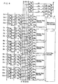
- Fig. 4 shows a fourth embodiment of the invetnion for solving such a problem.
- Fig. 4 is a combination of the conventional redundancy circuit shown in Fig. 5 and the redundancy circuit of the first embodiment shown in Fig. 1.
- the first column addresses are fed to a first column decoder 15. Concerning these first column addresses, a redundancy circuit using a redundancy column decoder 16 is realized. This is same as the conventional redundancy circuit shown in Fig. 5.
- the second column addresses are fed to the second column decoders 10, 11, 12, 13. Concerning these second column addresses, the circuit shown in the upper part of Fig. 4, that is, the same redundancy circuit as in the embodiment in Fig. 1 is added.
- the redundancy circuit portion of the embodiment in Fig. 4 may be replaced by the redundancy circuit shown in the embodiment in Fig. 2, or, needless to say, the internal structure of the second column decoders 10 to 14 in the embodiment in Fig. 4 may be constructed same as in the embodiment in Fig. 3.
Landscapes
- For Increasing The Reliability Of Semiconductor Memories (AREA)
- Techniques For Improving Reliability Of Storages (AREA)
- Dram (AREA)
Applications Claiming Priority (2)
| Application Number | Priority Date | Filing Date | Title |
|---|---|---|---|
| JP3159/89 | 1989-01-10 | ||
| JP315989 | 1989-01-10 |
Publications (3)
| Publication Number | Publication Date |
|---|---|
| EP0378332A2 true EP0378332A2 (de) | 1990-07-18 |
| EP0378332A3 EP0378332A3 (de) | 1992-05-27 |
| EP0378332B1 EP0378332B1 (de) | 1996-04-03 |
Family
ID=11549573
Family Applications (1)
| Application Number | Title | Priority Date | Filing Date |
|---|---|---|---|
| EP19900300175 Expired - Lifetime EP0378332B1 (de) | 1989-01-10 | 1990-01-08 | Halbleiterspeichergerät mit Redundanzschaltungen |
Country Status (2)
| Country | Link |
|---|---|
| EP (1) | EP0378332B1 (de) |
| DE (1) | DE69026289T2 (de) |
Families Citing this family (1)
| Publication number | Priority date | Publication date | Assignee | Title |
|---|---|---|---|---|
| CN114121123B (zh) * | 2021-11-30 | 2025-05-06 | 深圳市嘉合劲威电子科技有限公司 | 一种单晶内存修补双晶内存的方法和装置 |
Family Cites Families (4)
| Publication number | Priority date | Publication date | Assignee | Title |
|---|---|---|---|---|
| JPS58130495A (ja) * | 1982-01-29 | 1983-08-03 | Toshiba Corp | 半導体記憶装置 |
| US4471472A (en) * | 1982-02-05 | 1984-09-11 | Advanced Micro Devices, Inc. | Semiconductor memory utilizing an improved redundant circuitry configuration |
| US4573146A (en) * | 1982-04-20 | 1986-02-25 | Mostek Corporation | Testing and evaluation of a semiconductor memory containing redundant memory elements |
| FR2611301B1 (fr) * | 1987-02-24 | 1989-04-21 | Thomson Semiconducteurs | Memoire integree avec redondance de colonnes de donnees |
-
1990
- 1990-01-08 EP EP19900300175 patent/EP0378332B1/de not_active Expired - Lifetime
- 1990-01-08 DE DE1990626289 patent/DE69026289T2/de not_active Expired - Fee Related
Also Published As
| Publication number | Publication date |
|---|---|
| DE69026289T2 (de) | 1996-10-31 |
| EP0378332B1 (de) | 1996-04-03 |
| DE69026289D1 (de) | 1996-05-09 |
| EP0378332A3 (de) | 1992-05-27 |
Similar Documents
| Publication | Publication Date | Title |
|---|---|---|
| US5255228A (en) | Semiconductor memory device with redundancy circuits | |
| JP2798497B2 (ja) | メモリ回路 | |
| EP0146357B1 (de) | Halbleiterspeichergerät | |
| US4837747A (en) | Redundary circuit with a spare main decoder responsive to an address of a defective cell in a selected cell block | |
| EP0099910B1 (de) | Halbleiterspeicher mit redundanter schaltung | |
| US4459685A (en) | Redundancy system for high speed, wide-word semiconductor memories | |
| US5617365A (en) | Semiconductor device having redundancy circuit | |
| US5126973A (en) | Redundancy scheme for eliminating defects in a memory device | |
| US4648075A (en) | Redundancy circuit for a semiconductor memory device | |
| EP0549193A2 (de) | Nichtflüchtiger Halbleiterspeichergerät mit Redundanz | |
| US20130010538A1 (en) | Memory device and method for repairing a semiconductor memory | |
| US5265055A (en) | Semiconductor memory having redundancy circuit | |
| JPH1040694A (ja) | 半導体記憶装置 | |
| KR970076893A (ko) | 비휘발성 집적회로용 리던던시 방법 및 장치 | |
| US6055196A (en) | Semiconductor device with increased replacement efficiency by redundant memory cell arrays | |
| US4485459A (en) | Redundant columns for byte wide memories | |
| US4672581A (en) | Repairable memory array | |
| US4937790A (en) | Semiconductor memory device | |
| US7218558B2 (en) | Semiconductor memory devices having column redundancy circuits therein that support multiple memory blocks | |
| US20020085431A1 (en) | Redundancy circuit of semiconductor memory device | |
| KR0140350B1 (ko) | 반도체 기억 장치 | |
| KR100338412B1 (ko) | 다중 복구 크기의 리던던시 | |
| JP3862220B2 (ja) | 半導体記憶装置 | |
| US6535436B2 (en) | Redundant circuit and method for replacing defective memory cells in a memory device | |
| KR0172382B1 (ko) | 메모리셀 어레이 블럭의 재배치가 가능한 반도체 메모리 장치 |
Legal Events
| Date | Code | Title | Description |
|---|---|---|---|
| PUAI | Public reference made under article 153(3) epc to a published international application that has entered the european phase |
Free format text: ORIGINAL CODE: 0009012 |
|
| AK | Designated contracting states |
Kind code of ref document: A2 Designated state(s): DE FR GB NL |
|
| PUAL | Search report despatched |
Free format text: ORIGINAL CODE: 0009013 |
|
| AK | Designated contracting states |
Kind code of ref document: A3 Designated state(s): DE FR GB NL |
|
| 17P | Request for examination filed |
Effective date: 19920709 |
|
| 17Q | First examination report despatched |
Effective date: 19940803 |
|
| GRAA | (expected) grant |
Free format text: ORIGINAL CODE: 0009210 |
|
| AK | Designated contracting states |
Kind code of ref document: B1 Designated state(s): DE FR GB NL |
|
| PG25 | Lapsed in a contracting state [announced via postgrant information from national office to epo] |
Ref country code: NL Free format text: LAPSE BECAUSE OF FAILURE TO SUBMIT A TRANSLATION OF THE DESCRIPTION OR TO PAY THE FEE WITHIN THE PRESCRIBED TIME-LIMIT Effective date: 19960403 Ref country code: FR Effective date: 19960403 |
|
| REF | Corresponds to: |
Ref document number: 69026289 Country of ref document: DE Date of ref document: 19960509 |
|
| EN | Fr: translation not filed | ||
| NLV1 | Nl: lapsed or annulled due to failure to fulfill the requirements of art. 29p and 29m of the patents act | ||
| PLBE | No opposition filed within time limit |
Free format text: ORIGINAL CODE: 0009261 |
|
| STAA | Information on the status of an ep patent application or granted ep patent |
Free format text: STATUS: NO OPPOSITION FILED WITHIN TIME LIMIT |
|
| 26N | No opposition filed | ||
| REG | Reference to a national code |
Ref country code: GB Ref legal event code: IF02 |
|
| PGFP | Annual fee paid to national office [announced via postgrant information from national office to epo] |
Ref country code: GB Payment date: 20020109 Year of fee payment: 13 |
|
| PGFP | Annual fee paid to national office [announced via postgrant information from national office to epo] |
Ref country code: DE Payment date: 20020212 Year of fee payment: 13 |
|
| REG | Reference to a national code |
Ref country code: GB Ref legal event code: 732E |
|
| PG25 | Lapsed in a contracting state [announced via postgrant information from national office to epo] |
Ref country code: GB Free format text: LAPSE BECAUSE OF NON-PAYMENT OF DUE FEES Effective date: 20030108 |
|
| PG25 | Lapsed in a contracting state [announced via postgrant information from national office to epo] |
Ref country code: DE Free format text: LAPSE BECAUSE OF NON-PAYMENT OF DUE FEES Effective date: 20030801 |
|
| GBPC | Gb: european patent ceased through non-payment of renewal fee |
Effective date: 20030108 |