EP0378439B1 - Aufzeichnungskopf - Google Patents
Aufzeichnungskopf Download PDFInfo
- Publication number
- EP0378439B1 EP0378439B1 EP90300381A EP90300381A EP0378439B1 EP 0378439 B1 EP0378439 B1 EP 0378439B1 EP 90300381 A EP90300381 A EP 90300381A EP 90300381 A EP90300381 A EP 90300381A EP 0378439 B1 EP0378439 B1 EP 0378439B1
- Authority
- EP
- European Patent Office
- Prior art keywords
- region
- head
- type
- transistor
- electric
- Prior art date
- Legal status (The legal status is an assumption and is not a legal conclusion. Google has not performed a legal analysis and makes no representation as to the accuracy of the status listed.)
- Expired - Lifetime
Links
- 239000004065 semiconductor Substances 0.000 claims abstract description 89
- 239000000758 substrate Substances 0.000 claims abstract description 60
- 238000002955 isolation Methods 0.000 claims description 40
- 239000012535 impurity Substances 0.000 claims description 30
- 239000011159 matrix material Substances 0.000 claims description 8
- 238000007599 discharging Methods 0.000 claims description 6
- 239000010408 film Substances 0.000 claims 1
- 239000010409 thin film Substances 0.000 claims 1
- VYPSYNLAJGMNEJ-UHFFFAOYSA-N Silicium dioxide Chemical compound O=[Si]=O VYPSYNLAJGMNEJ-UHFFFAOYSA-N 0.000 description 41
- 238000000034 method Methods 0.000 description 32
- 239000007788 liquid Substances 0.000 description 28
- 239000010410 layer Substances 0.000 description 22
- 238000010276 construction Methods 0.000 description 16
- XUIMIQQOPSSXEZ-UHFFFAOYSA-N Silicon Chemical compound [Si] XUIMIQQOPSSXEZ-UHFFFAOYSA-N 0.000 description 15
- 229910052710 silicon Inorganic materials 0.000 description 15
- 239000010703 silicon Substances 0.000 description 15
- 229910052814 silicon oxide Inorganic materials 0.000 description 15
- 229910052681 coesite Inorganic materials 0.000 description 13
- 229910052906 cristobalite Inorganic materials 0.000 description 13
- 238000010586 diagram Methods 0.000 description 13
- 239000000377 silicon dioxide Substances 0.000 description 13
- 235000012239 silicon dioxide Nutrition 0.000 description 13
- 229910052682 stishovite Inorganic materials 0.000 description 13
- 229910052905 tridymite Inorganic materials 0.000 description 13
- 150000002500 ions Chemical class 0.000 description 12
- 238000004544 sputter deposition Methods 0.000 description 11
- 238000009792 diffusion process Methods 0.000 description 10
- 230000003071 parasitic effect Effects 0.000 description 10
- 239000011241 protective layer Substances 0.000 description 10
- 230000000694 effects Effects 0.000 description 8
- 230000003321 amplification Effects 0.000 description 7
- 230000007257 malfunction Effects 0.000 description 7
- 238000003199 nucleic acid amplification method Methods 0.000 description 7
- 238000009825 accumulation Methods 0.000 description 6
- 230000020169 heat generation Effects 0.000 description 6
- 239000011229 interlayer Substances 0.000 description 6
- 230000002829 reductive effect Effects 0.000 description 6
- 230000007423 decrease Effects 0.000 description 5
- 230000003247 decreasing effect Effects 0.000 description 5
- 238000002474 experimental method Methods 0.000 description 5
- 238000001039 wet etching Methods 0.000 description 5
- 229910003862 HfB2 Inorganic materials 0.000 description 4
- 239000004642 Polyimide Substances 0.000 description 4
- 229920001721 polyimide Polymers 0.000 description 4
- 230000001681 protective effect Effects 0.000 description 4
- 230000000630 rising effect Effects 0.000 description 4
- 238000009835 boiling Methods 0.000 description 3
- 238000005530 etching Methods 0.000 description 3
- 239000011368 organic material Substances 0.000 description 3
- 238000007254 oxidation reaction Methods 0.000 description 3
- 229910052698 phosphorus Inorganic materials 0.000 description 3
- 229920001296 polysiloxane Polymers 0.000 description 3
- 239000000956 alloy Substances 0.000 description 2
- 229910045601 alloy Inorganic materials 0.000 description 2
- 229910052785 arsenic Inorganic materials 0.000 description 2
- 239000011521 glass Substances 0.000 description 2
- 238000005468 ion implantation Methods 0.000 description 2
- 230000000670 limiting effect Effects 0.000 description 2
- 238000004519 manufacturing process Methods 0.000 description 2
- 230000003647 oxidation Effects 0.000 description 2
- 238000000059 patterning Methods 0.000 description 2
- 239000000843 powder Substances 0.000 description 2
- 239000011347 resin Substances 0.000 description 2
- 229920005989 resin Polymers 0.000 description 2
- OAICVXFJPJFONN-UHFFFAOYSA-N Phosphorus Chemical compound [P] OAICVXFJPJFONN-UHFFFAOYSA-N 0.000 description 1
- 230000002411 adverse Effects 0.000 description 1
- 230000000593 degrading effect Effects 0.000 description 1
- 238000000151 deposition Methods 0.000 description 1
- 230000008021 deposition Effects 0.000 description 1
- 230000010354 integration Effects 0.000 description 1
- 231100000989 no adverse effect Toxicity 0.000 description 1
- 239000011574 phosphorus Substances 0.000 description 1
- 238000000206 photolithography Methods 0.000 description 1
- 230000002441 reversible effect Effects 0.000 description 1
Images


Classifications
-
- B—PERFORMING OPERATIONS; TRANSPORTING
- B41—PRINTING; LINING MACHINES; TYPEWRITERS; STAMPS
- B41J—TYPEWRITERS; SELECTIVE PRINTING MECHANISMS, i.e. MECHANISMS PRINTING OTHERWISE THAN FROM A FORME; CORRECTION OF TYPOGRAPHICAL ERRORS
- B41J2/00—Typewriters or selective printing mechanisms characterised by the printing or marking process for which they are designed
- B41J2/005—Typewriters or selective printing mechanisms characterised by the printing or marking process for which they are designed characterised by bringing liquid or particles selectively into contact with a printing material
- B41J2/01—Ink jet
- B41J2/135—Nozzles
- B41J2/14—Structure thereof only for on-demand ink jet heads
- B41J2/14016—Structure of bubble jet print heads
- B41J2/14088—Structure of heating means
- B41J2/14112—Resistive element
- B41J2/14129—Layer structure
-
- B—PERFORMING OPERATIONS; TRANSPORTING
- B41—PRINTING; LINING MACHINES; TYPEWRITERS; STAMPS
- B41J—TYPEWRITERS; SELECTIVE PRINTING MECHANISMS, i.e. MECHANISMS PRINTING OTHERWISE THAN FROM A FORME; CORRECTION OF TYPOGRAPHICAL ERRORS
- B41J2/00—Typewriters or selective printing mechanisms characterised by the printing or marking process for which they are designed
- B41J2/005—Typewriters or selective printing mechanisms characterised by the printing or marking process for which they are designed characterised by bringing liquid or particles selectively into contact with a printing material
- B41J2/01—Ink jet
- B41J2/135—Nozzles
- B41J2/16—Production of nozzles
- B41J2/1601—Production of bubble jet print heads
- B41J2/1604—Production of bubble jet print heads of the edge shooter type
-
- B—PERFORMING OPERATIONS; TRANSPORTING
- B41—PRINTING; LINING MACHINES; TYPEWRITERS; STAMPS
- B41J—TYPEWRITERS; SELECTIVE PRINTING MECHANISMS, i.e. MECHANISMS PRINTING OTHERWISE THAN FROM A FORME; CORRECTION OF TYPOGRAPHICAL ERRORS
- B41J2/00—Typewriters or selective printing mechanisms characterised by the printing or marking process for which they are designed
- B41J2/005—Typewriters or selective printing mechanisms characterised by the printing or marking process for which they are designed characterised by bringing liquid or particles selectively into contact with a printing material
- B41J2/01—Ink jet
- B41J2/135—Nozzles
- B41J2/16—Production of nozzles
- B41J2/1621—Manufacturing processes
- B41J2/1626—Manufacturing processes etching
- B41J2/1629—Manufacturing processes etching wet etching
-
- B—PERFORMING OPERATIONS; TRANSPORTING
- B41—PRINTING; LINING MACHINES; TYPEWRITERS; STAMPS
- B41J—TYPEWRITERS; SELECTIVE PRINTING MECHANISMS, i.e. MECHANISMS PRINTING OTHERWISE THAN FROM A FORME; CORRECTION OF TYPOGRAPHICAL ERRORS
- B41J2/00—Typewriters or selective printing mechanisms characterised by the printing or marking process for which they are designed
- B41J2/005—Typewriters or selective printing mechanisms characterised by the printing or marking process for which they are designed characterised by bringing liquid or particles selectively into contact with a printing material
- B41J2/01—Ink jet
- B41J2/135—Nozzles
- B41J2/16—Production of nozzles
- B41J2/1621—Manufacturing processes
- B41J2/164—Manufacturing processes thin film formation
- B41J2/1642—Manufacturing processes thin film formation thin film formation by CVD [chemical vapor deposition]
-
- B—PERFORMING OPERATIONS; TRANSPORTING
- B41—PRINTING; LINING MACHINES; TYPEWRITERS; STAMPS
- B41J—TYPEWRITERS; SELECTIVE PRINTING MECHANISMS, i.e. MECHANISMS PRINTING OTHERWISE THAN FROM A FORME; CORRECTION OF TYPOGRAPHICAL ERRORS
- B41J2/00—Typewriters or selective printing mechanisms characterised by the printing or marking process for which they are designed
- B41J2/005—Typewriters or selective printing mechanisms characterised by the printing or marking process for which they are designed characterised by bringing liquid or particles selectively into contact with a printing material
- B41J2/01—Ink jet
- B41J2/135—Nozzles
- B41J2/16—Production of nozzles
- B41J2/1621—Manufacturing processes
- B41J2/164—Manufacturing processes thin film formation
- B41J2/1646—Manufacturing processes thin film formation thin film formation by sputtering
-
- B—PERFORMING OPERATIONS; TRANSPORTING
- B41—PRINTING; LINING MACHINES; TYPEWRITERS; STAMPS
- B41J—TYPEWRITERS; SELECTIVE PRINTING MECHANISMS, i.e. MECHANISMS PRINTING OTHERWISE THAN FROM A FORME; CORRECTION OF TYPOGRAPHICAL ERRORS
- B41J2202/00—Embodiments of or processes related to ink-jet or thermal heads
- B41J2202/01—Embodiments of or processes related to ink-jet heads
- B41J2202/13—Heads having an integrated circuit
Definitions
- the present invention relates to a recording head for use in, for example, a copier, a facsimile, wordprocessor, an output printer of terminal of host computer, or video output printer. More particularly, the invention relates to a recording head and recording apparatus wherein an electrothermal converting element and a driving element are formed on a common substrate.
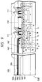
- Fig. 1A shows an example of such a semiconductor device.
- reference numeral 24 denotes an insulative substrate; 25 a semiconductor substrate; 26 an anode semiconductor region; 27 a cathode region.
- the above semiconductor device has a feature such that it has a construction in which individual diodes are respectively arranged at intervals on the insulative substrate and are adhered thereto. Since the device has the above construction, a degree of freedom for a requirement of the standards for the diodes is large and a proper diode can be selected in a wide range in accordance with the use object. Further, since an electrical mutual interference between the diodes can be prevented, a high reverse bias voltage can be blocked by the insulative substrate and a large current can be supplied and a semiconductor device which has a high withstanding voltage and can endure a large current is realized.
- Fig. 1B is a diagram showing an example of an electric circuit using the semiconductor device shown in Fig. 1A.
- a switch 29 is closed, a positive potential H1 is biased, and further, a switch 30 is closed, thereby turning on a diode 31 corresponding to the segment to be supplied with a current.
- a switch 30 is closed, thereby turning on a diode 31 corresponding to the segment to be supplied with a current.
- Respective segments such as electrothermal converting elements, are electrically connected to respective diodes so that the segment can be solely made operative.
- the above-mentioned semiconductor device is used in a recording head such as an ink jet recording head comprising a discharge opening to discharge an ink, a liquid passage communicated with the discharge port, and an electrical/thermal converting element serving as a discharge energy generating element which is provided within inside of or outside of a liquid path in correspondence to the discharge port or in a thermal head which is used for thermal copy transfer recording, thermal recording, or the like
- a recording head such as an ink jet recording head comprising a discharge opening to discharge an ink, a liquid passage communicated with the discharge port, and an electrical/thermal converting element serving as a discharge energy generating element which is provided within inside of or outside of a liquid path in correspondence to the discharge port or in a thermal head which is used for thermal copy transfer recording, thermal recording, or the like
- the present inventors have found the fact from many experiments that the construction of the recording head must be determined by sufficiently considering an influence by the heat which is generated in the semiconductor device, an influence by the heat generation of the electrical/thermal converting element, and the like in order to use a liquid (ink).
- the present invention is made in consideration of the foregoing technical subjects.
- an ink jet recording head comprising: a discharge port for discharging ink; an electric/thermal converting element for generating thermal energy; and a transistor element provided and connected for driving the electric/thermal converting element; wherein the electric/thermal converting element and the transistor element are formed on a semiconductor substrate; characterised in that a base and a collector of the transistor element are short-circuited and electrically connected to the electric/thermal converting element.
- an ink jet recording head comprising: a discharge port for discharging ink; an electric/thermal converting element for generating thermal energy; and a transistor element provided and connected for driving the electric/thermal converting element; wherein the electric/thermal converting element and the transistor element are formed on a semiconductor substrate; characterised in that a base and a collector of the transistor element are short-circuited and an emitter of the transistor element is electrically connected to the electric/thermal converting element.
- an ink jet recording apparatus as set out in claim 16.
- Embodiments of the invention provide a semiconductor device of low cost which can be relatively easily manufactured.
- Embodiments of the invention provide, in particular, a semiconductor device having a plurality of elements in which a variation among the elements is suppressed and the device comprises uniform elements.
- Embodiments of the invention provide a miniaturized semiconductor device having a high degree of integration.
- Embodiments of the invention provide an efficient semiconductor device which can suppress a leakage current due to a parasitic PN junction structure.
- Embodiments of the invention provide, in particular, a semiconductor device having a plurality of elements in which an influence on the adjacent element is prevented and a malfunction of the device does not occur.
- Embodiments of the invention provide a recording head which has excellent discharging characteristics and can record at a high speed with a high resolution.
- Embodiments of the present invention provide, as a means for solving above described problem, a recording head having a semiconductor substrate, transistor elements provided on the semiconductor substrate, and electrical/thermal converting elements provided on the semiconductor substrate, wherein the recording head has a first wiring electrode in which a base and a collector of each transistor element are short-circuited, a second wiring electrode which is electrically connected to the semiconductor substrate, and a third wiring electrode which is connected to one of electrodes of the electrical/thermal converting elements, and an emitter of the transistor element and the other electrode of the electrical/thermal converting elements are electrically connected.
- Embodiments of the present invention provide a recording head comprising: a semiconductor substrate; transistor elements provided on the semiconductor substrates; and electrical/thermal converting elements provided on the semiconductor substrate, wherein the recording head has a first wiring electrode which is electrically connected to one of a pair of electrodes of the electrical/thermal converting elements and a second wiring electrode which is electrically connected to the emitters of the transistor elements, and the base and the collector of each transistor element are short-circuited and are electrically connected to the other one of the pair of the electrodes of the electrical/thermal converting elements.
- the high density, high performance, and miniaturization of the recording head can be realized by low costs.
- the collector and the base of the transistor for driving the energy generating elements are electrically short-circuited, even if there is a variation among current amplification factors of the transistors forming a plurality of diodes, a current concentration does not occur in the diode having a predetermined large current amplification factor. Thus, the energy generating elements and the semiconductor elements are not destroyed.
- the semiconductor elements and the energy generating elements can be formed on the same substrate and the high density, high performance, and miniaturization of the recording head can be realized. Further, according to a circuit construction of the embodiment, a liquid droplet which is always stable and has excellent discharge response characteristics can be formed at a high speed.
- a liquid droplet which is always stable can be formed with excellent response and with high speed.
- Fig. 2A is a schematic sectional view showing a functional element for use in a recording head in an embodiment of the present invention.
- reference numeral 1 denotes an N type silicon substrate; 2 an N type epitaxial region constructing elements; 3 a P type collector buried region constituting the elements; 4 an N type isolation region to isolate elements; 5 a P type collector region constructing the elements; 6 an N type isolation region to isolate the elements; 7 an high concentration P type emitter region constructing the elements; 8 an N type base region of a high concentration constructing the elements; 9 a P type isolation region of a high concentration constituting the elements; 10 an N type isolation region isolating the elements.
- Such functional element operates such that, by forwardly biasing (V H1 ) an electrode 11 by applying biases (V H1 ) of positive potentials to the electrode 11, the PNP transistor in the cell is turned on and bias currents flow out of the emitter electrode 11 as a collector current and a base current.
- V H1 forwardly biasing
- V H1 biases
- the recording head is desirably driven.
- high speed switching property which recording head required is obtained. Rising property is desirable. Parasitic effect is relatively small. Accordingly, variation among the elements are small. And stable drive current can be obtained.
- the isolation region is not connected to the ground.
- Fig. 3 is a diagram showing an equivalent circuit of the semiconductor device together with parasitic effect shown in Fig. 2.
- R C denotes the internal resistance of the collector region
- R B indicates the internal resistance of the base region
- R S represents a resistance of the N type silicon substrate 1.
- T r1 corresponds to a PNP transistor which is formed by the P type emitter region 7, N type epitaxial region 2, and P type collector buried region 3.
- T r2 corresponds to an NPN transistor which is formed by the N type epitaxial region 2, P type collector buried region 3, and N type silicon substrate.
- T r3 corresponds to a parasitic PNP parasitic transistor which is formed by the P type collector buried regions 3 and N type silicon substrate 1 of the adjacent cells.
- R C , R B , and R S can be set to large values by, for instance, reducing the concentrations of the collector region, base region, and N type silicon substrate 1.
- the impurity concentrations were set to values within a range from 1 x 10¹⁵ to 1 x 1017 cm ⁇ 3.
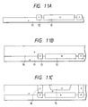
- Fig. 4A is a diagrammatical perspective view showing an ink jet recording head according to an embodiment of the invention.
- Reference numeral 500 denotes a discharge port to discharge an ink and 501 indicates a liquid passage wall member to form a liquid passage communicating with the discharge port 500.
- the liquid passage wall member 501 is formed by a photo sensitive resin or the like.
- Reference numeral 502 indicates a top plate formed by glass, resin, or the like and 503 represents a supply port of a liquid.
- Fig. 4B is a diagrammatical cross sectional view taken along the line E-E' in Fig. 4A showing the ink jet recording head having a drive section of the semiconductor element mentioned above.
- the liquid passage wall member 501 and the top plate 502 are omitted for simple explanation.
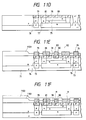
- Fig. 5 is a diagram for explaining a method of driving the recording head shown in Figs. 4A and 4B.
- an SiO2 film 101 which has the above drive section and is formed by the thermal oxidation is formed on the substrate.
- An electric/thermal converting element which is formed by a heat generation resistance layer 103 made of HfB2 or the like and an electrode 104 made of Al or the like is provided on a heat accumulation layer 102 comprising an SiO2 film or the like which is formed by a sputtering process on the oxide film.
- an insulating protective film 105 made of SiO2 or the like and an anti cavitation protective film 106 made of Ta or the like which are formed by the sputtering process are provided on and over a heat generating portion 110 of the electric/thermal converting element.
- the SiO2 film formed by sputtering and forming the heat accumulation layer 102 is formed integrally with an interlayer insulative film between wirings 201 and 203 of the drive section.
- the film is similarly formed integrally with an interlayer insulative film between the wirings 201 and 202.
- a protective layer 107 made of an organic material such as photo sensitive polyimide or the like is provided as an insulative film having an excellent recording liquid resistance onto the wiring 202 of the top portion in the drive section.
- the recording head can be also constructed in a manner such that a top plate with grooves, an orifice plate, and the like are arranged to form the liquid passage and discharge port although they are not shown.
- the recording head can be also constructed in a manner such that the liquid is discharged in the direction which crosses the heat generating surface, for example, vertical direction.
- Fig. 5 The method of driving the recording head will now be described in detail with reference to Fig. 5. Although only two cells have been shown in Fig. 5, a proper number of, e.g., 128 cells as mentioned above are arranged and electrically connected like a M x N matrix.
- a desired group is selected by a switch G1, for example, at device body side and the electrothermal converting element RH1 of the recording head is selected by a switch S1 at device body side.
- a diode cell SH1 with a transistor construction is forwardly biased, a current is supplied, and the electrothermal converting element RH1 generates a heat.
- a heat energy causes a state change of the liquid, so that film boiling effect is caused and an air bubble is generated and the liquid is discharged from the discharge port.
- a wiring 203 which is electrically connected to the substrate 1 through the isolation region 4 was formed.
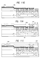
- An SiO2 film 102 serving as a heat accumulation layer and an interlayer insulative film was formed onto the whole surface by the sputtering process until a thickness of about 1.0 ⁇ m. (The above processes correspond to Fig. 6D)
- HfB2 of a thickness of about 1000 ⁇ was deposited as a heat generation resistance layer 103.
- a pair of electrodes 104a and 104b of the electric/thermal converting element and Al wirings serving as an anode electrode wiring 201 and a cathode electrode wiring 202 of the diode were deposited onto the heat generation resistance layer 103 and patterned.
- an SiO2 film 105 as a protective layer of the electric/thermal converting element and as an insulative layer between the Al wirings was deposited by the sputtering process. Contact holes were formed.
- the cathode electrode wiring 202 was formed.
- a Ta layer of a thickness of about 2000 ⁇ as a protective layer for the anti-cavitation was deposited in the upper portion of the heat generating section of the electric/thermal converting element.
- photo sensitive polyimide as a protective layer was formed onto the SiO2 film 105 and cathode electrode wiring 202. (The above processes correspond to Fig. 6F)
- a recording head as shown in Fig. 4A was manufactured by arranging the liquid passage wall member and the top plate to the substrate having the electric/thermal converting element and the semiconductor element which had been formed as mentioned above.
- the cells having a plurality of elements of Fig. 2B were connected like a matrix and the operation experiments were executed. Even when a current of 300 mA (total 2.4 A) was allowed to flow through each of eight semiconductor diodes, the other diodes did not cause a malfunction and a liquid droplet could be preferably discharged.
- a plurality of semiconductor elements each having a high withstanding voltage and each of which is excellent in electrical isolation performance every element can be formed on the single substrate. Therefore, for instance, in the circuit comprising the semiconductor elements which were connected like a matrix, there is no need to individually connect the elements from the outside and the number of steps can be reduced. Thus, the number of failure occurrence positions can be decreased and the high reliability can be assured.
- the semiconductor element and the electric/thermal converting element which is driven by the semiconductor element can be formed on the same substrate. Therefore, it is possible to obtain the recording head in which the area of the circuit can be reduced, the number of steps can be decreased, the reliability can be improved, and a recording image of a high resolution can be formed.
- the embodiment can be applied to semiconductor devices in various application fields. For instance, the embodiment can be also applied as a diode for a micro current. The embodiment can be also applied to a diode for a large current.
- the semiconductor device of the embodiment is excellent in a withstanding voltage and can be used by a large current. Therefore, the most typical advantages of the embodiment can be obtained in the case where it is used as a device for a large current.
- a drive voltage is applied to an emitter, a base and a collector are short-circuited, and an electric/thermal converting element is connected, since no minority carrier enters between the base and collector, the switching speed is high, the rising speed is improved, the parasitic effect is also lightened, a thermal energy suitable for a liquid can be applied, and good discharge characteristics can be obtained.
- Fig. 7A shows a driving portion for driving the recording head according to an embodiment of the present invention.
- reference numeral 71 denotes a P type silicon substrate; 72 an N type collector buried region constructing elements; 73 a P type isolation buried region to separate the elements; 74 an N type epitaxial region; 75 a P type base region constructing the elements; 76 a P type isolation region to separate the elements; 77 an N type collector region constructing the elements; 78 a P type base region of a high concentration constructing the elements; 79 a P type isolation region of a high concentration to separate the elements; 80 an N type emitter region constructing the elements; 81 an N type collector region of a high concentration constructing the elements; 82 a collector/base common electrode; 83 an emitter electrode; and 84 an isolation electrode.
- An NPN transistor is formed by the N type collector buried region 72, P type base region 75, and N type emitter region 80.
- the collector region is formed so as to completely surround the emitter region 80 and the base regions 75 and 78 by the regions 72, 77, and 81.
- an isolation region is formed as an element separating region by the P type isolation buried region, P type isolation region 77, and high concentration P type isolation region.
- a plurality of cells mentioned above are formed like a matrix.
- Fig. 7B is a circuit diagram showing a circuit construction of the semiconductor device according to the embodiment.
- the collector/base common electrode 82 corresponds to an anode of the diode and the emitter electrode 83 corresponds to a cathode of the diode. That is, by applying biases (V H1 ) of positive potentials to the collector/base common electrode 82, the NPN transistor in the cell is turned on and bias currents flow out of the emitter electrode 83 as a collector current and a base current.
- V H1 biases
- a concentration of the N type collector buried region 72 it is desirable to set a concentration of the N type collector buried region 72 to a value of 1 x 1019 cm ⁇ 3 or more.
- a concentration of the base region 75 it is desirable to set a concentration of the base region 75 to a value within a range from 1 x 1013 cm ⁇ 3 to 1 x 1015 cm ⁇ 3.
- Fig. 8 is a diagram showing an equivalent circuit of the semiconductor device shown in Fig. 7A.
- R d denotes an internal resistance of the collector region (the region comprising the N type collector buried region 72, N type collector region 77, and high concentration N type collector region 81) and R B indicates an internal resistance of the base region (the region comprising the P type base region 75 and high concentration P type base region 78), respectively.
- T r1 corresponds to an NPN transistor which is formed by the N type collector buried region 72, P type base region 75, and N type emitter region 80.
- T r2 indicates a PNP transistor which is formed by the P type base region 75, N type collector buried region 72, and P type silicone substrate 71. That is, T r2 represents a transistor structure which results in a cause of the leakage current.
- the countermeasure 1 will be first described.
- R B ⁇ ⁇ 1 ⁇ R C is necessary.
- the resistance (R C ) of the collector region is reduced, for example, by increasing the concentration of the N type collector buried region 72.
- the concentration of the high concentration P type base region 78 is reduced or the area of the base region 78 is decreased.
- the countermeasure 2 will now be described.
- the leakage current to the P type silicon substrate 71 can be suppressed.
- the current amplification factor ⁇ 2 of the transistor T r2 it is sufficient to increase the concentration of the base region (N type collector buried region 72) of the T r2 .
- the method whereby the concentration of the N type collector buried region 72 is increased has an effect for both of the countermeasures 1 and 2.
- the impurity concentration of the N type collector buried region 72 was set to 1 x 1019 cm ⁇ 3 or more and, further, the impurity concentration of the P type base region 75 was set to a value within a range from 1 x 1013 cm ⁇ 3 to 1 x 1015 cm ⁇ 3.
- Fig. 4A is a diagrammatical perspective view showing an ink jet recording head according to the embodiment.
- Fig. 9 is a diagrammatical cross sectional view taken along the line E-E' in Fig. 4A showing the ink jet recording head having a drive section of the semiconductor element mentioned above.
- Fig. 10 is a diagram for explaining a method of driving the recording head shown in Fig. 9.
- an SiO2 film 1101 which has the above function element and is formed by the thermal oxidation is formed on the substrate.
- An electric/thermal converting element which is formed by a heat generation resistance layer 1103 made of HfB2 or the like and an electrode 1104 made of Al or the like is provided on a heat accumulation layer 1102 comprising an SiO2 film or the like which is formed by a sputtering process.
- a protective film 1105 made of SiO2 or the like and a protective film 1106 made of Ta or the like which are formed by the sputtering process are provided on and over a heat generating portion 1110 of the electric/thermal converting element.
- the SiO2 film forming the one heat accumulation layer 1102 of the two is formed integrally with an interlayer insulative film 1102 between wirings 82, 83, 84 and wiring 1104 of the electrothermal converting element, second layer wiring, of the drive section, lower wiring.
- the film is similarly formed integrally with an interlayer insulative film 1105' between the second wiring 1104 and upper layer wiring 1111.
- a protective layer 1107 made of an organic material such as photo sensitive polyimide or the like is provided as an insulative film having an excellent recording liquid resistance onto the wiring 1111 of the top portion in the drive section.
- the recording head can be also constructed in a manner such that a top plate with grooves, an orifice plate, and the like are arranged to form the liquid passage and discharge port although they are not shown.
- the recording head can be also constructed in a manner such that the liquid is discharged in the direction which crosses the heat generating surface.
- a desired group is selected by a switch G1 at the apparatus body and the electrothermal converting element RH1 is selected by for example a switch S1 at the apparatus body.
- a diode cell SH1 with a transistor construction is forwardly biased, a current is supplied, and the electrothermal converting element RH1 of the recording head generates a heat.
- a heat energy causes a state change of the liquid, so that film boiling effect is occured and an air bubble is generated and the liquid is discharged from the discharge port.
- the switches G1, for example, at apparatus body and S2 are selectively turned on, a diode cell SH2 at recording head is driven, and a current is supplied to the electrothermal converting element RH2.
- the isolation electrode 84 is maintained at ground potential, thereby the substrate is maintained at the ground potential via the isolation regions 73, 76, 79. Thus, each cell is isolated.
- the structure also achieves the following advantageous effect.
- the substrate 71 itself is partially exposed to outside or exposed via the member of conductive body. Thus, the operator is likely to touch the substrate 71.
- HfB2 of a thickness of about 1000 ⁇ was deposited and patterned as the heat generation resistance layer 1103.
- a pair of electrodes 1104, 1104′ of the electrothermal converting element are formed.
- Al is deposited by sputtering.
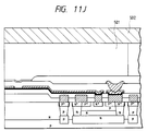
- desired electrical connection is obtained (Fig. 11G).
- the protective layer of the electrothermal converting element and silicon oxide film 1105 serves as an insulating layer between the intermediate wiring and upper wiring formed thereon are deposited by sputtering.
- through hole is formed at the silicon oxide film 1105 by etching. Again, by Al deposition and patterning, upper wiring 1111 connected to base/collector electrode 82 via the intermediate Al layer is formed.
- the isolation wiring is arranged at lower layer.
- the emitter (cathode) wiring and wiring of the electrothermal converting element are arranged at an intermediate positions.
- Base/collector (anode) wiring is arranged at upper most position.
- Three layer wiring structure wherein each one is connected via two holes (Fig. 11H).
- Ta layer 1106 of about 2000 ⁇ is formed on the upper portion of the electrothermal converting element.
- photo sensitive polyimide layer 1107 comprising organic material is formed (Fig. 11I).
- the recording head is manufactured by providing the substrate having the electrothermal converting element and the semiconductor elements with the liquid path wall member 501 and the upper board 502.
- the cells having a plurality of semiconductor elements of Fig. 7B were connected like a matrix and the operation experiments were executed.
- eight semiconductor diodes were connected to one segment and a current of 300 mA (total 2.4 A) was allowed to flow through each diode.
- the other semiconductor diodes did not cause a malfunction and a liquid droplet could be properly discharged.
- Embodiments of the invention can be also applied to a PNP transistor construction.
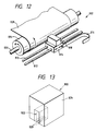
- Fig. 12 is a diagrammatical perspective view of an ink jet recording apparatus in which the recording head of an embodiment of the invention is installed.
- Means for conveying a recording paper 808 as a recording medium comrpises a platen roller 804 and a shaft 806 to rotate the platen roller in the direction indicated by an arrow A.
- An ink tank integrated type head 818 is mounted on a carriage 814 which is guided by two guide shafts 810 and 812 and is reciprocated. The head 818 executes the recording by discharging an ink while moving along the recording paper surface.
- Reference numeral 816 denotes a flexible cable to transmit a drive signal to drive the electrothermal converting element of the recording head and a bias signal to bias the semiconductor substrate and the isolation regions.
- Fig. 13 shows the recording head 818.
- the head shown in Fig. 4A is assembled in an ink tank 824.
- An electric connecting terminal 820 is arranged in the lower portion of the head 818.
- Reference numeral 822 denotes a plurality of discharge ports to discharge the ink.
- Reference numeral 838 denotes a carriage side connecting terminal which is electrically connected to the flexible cable and is coupled to the connecting terminal 820 of the head 818.
- Each of the carriage side connecting terminal 838 and the head side connecting terminal 820 includes a contact to transmit the drive signal and a contact to transmit the bias signal.
- the heads in the foregoing first and second embodiments and the head as an example of the construction shown in U.S.P. No. 4,429,321 which had been shown as a conventional example were prepared.
- Each of the heads was driven by the drive signal of 300 mA and a pulse width of 10 ⁇ sec and the dot deviations of the discharged ink droplets were evaluated.
- the evaluating method is as follows.
- a plurality of semiconductor elements each having a high withstanding voltage and each of which is excellent in electrical isolation performance every element can be formed on the single substrate. Therefore, for instance, in the circuit comprising the semiconductor elements which were connected like a matrix, there is no need to individually connect the elements from the outside and the number of steps can be reduced. Thus, the number of failure occurrence positions can be decreased and the high reliability can be assured.
- the semiconductor element and the electric/thermal converting element which is driven by the semiconductor element can be formed on the same substrate. Therefore, it is possible to obtain the recording head in which the area of the circuit can be reduced, the number of steps can be decreased, the reliability can be improved, and a recording image of a high resolution can be formed.
- the embodiment can be applied to semiconductor devices in various application fields. For instance, the embodiment can be also applied as a diode for a micro current. The embodiment can be also applied to a diode for a large current.
- the semiconductor device of the embodiment is excellent in a withstanding voltage and can be used by a large current. Therefore, the most typical advantages of the embodiment can be obtained in the case where it is used as a device for a large current.
- a drive voltage is applied to an emitter, a base and a collector are short-circuited, and an electric/thermal converting element is connected, since no minority carrier enters between the base and collector, the switching speed is high, the rising speed is improved, the parasitic effect is also lightened, a thermal energy suitable for a liquid can be applied, and good discharge characteristics can be obtained.
Landscapes
- Engineering & Computer Science (AREA)
- Manufacturing & Machinery (AREA)
- Particle Formation And Scattering Control In Inkjet Printers (AREA)
- Magnetic Heads (AREA)
Claims (16)
- Tintenstrahl-Aufzeichnungskopf (100, 818) mit
einer Ausstoßöffnung (500, 822) zum Ausstoßen von Tinte,
einem elektrothermischen Wandlerelement (103, 104, 1103, 1104) zum Erzeugen von Wärmeenergie und
einem Transistorelement, das zum Steuern des elektrothermischen Wandlerelements (103, 104, 1103, 1104) vorgesehen und angeschlossen ist,
wobei das elektrothermische Wandlerelement (103, 104, 1103, 1104) und das Transistorelement auf einem Halbleitersubstrat (1, 71) ausgebildet sind,
dadurch gekennzeichnet, daß
eine Basis und ein Kollektor des Transistorelements kurzgeschlossen und an das elektrothermische Wandlerelement (103, 104, 1103, 1104) elektrisch angeschlossen sind. - Tintenstrahl-Aufzeichnungskopf (100, 818) mit
einer Ausstoßöffnung (500, 822) zum Ausstoßen von Tinte,
einem elektrothermischen Wandlerelement (103, 104, 1103, 1104) zum Erzeugen von Wärmeenergie und
einem Transistorelement, das zum Steuern des elektrothermischen Wandlerelements (103, 104, 1103, 1104) vorgesehen und angeschlossen ist,
wobei das elektrothermische Wandlerelement (103, 104, 1103, 1104) und das Transistorelement auf einem Halbleitersubstrat (1, 71) ausgebildet sind,
dadurch gekennzeichnet, daß
eine Basis und ein Kollektor des Transistorelements kurzgeschlossen und ein Emitter des Transistorelements an das elektrothermische Wandlerelement (103, 104, 1103, 1104) elektrisch angeschlossen ist. - Aufzeichnungskopf (100, 818) nach Anspruch 2, dadurch gekennzeichnet, daß das Transistorelement
einen Kollektorbereich mit einem n-Halbleiter mit einer Störstellenkonzentration von 1 · 10¹⁹ cm⁻³ oder mehr und
einen Basisbereich mit einem p-Halbleiter mit einer Störstellenkonzentration enthält, die in einem Bereich von 1 · 10¹³ bis 1 · 10¹⁵ cm⁻³ liegt. - Aufzeichnungskopf (100, 818) nach Anspruch 1 oder 2, dadurch gekennzeichnet, daß das Transistorelement ein npn-Transistor ist.
- Aufzeichnungskopf (100, 818) nach Anspruch 1 oder 2, dadurch gekennzeichnet, daß das Transistorelement ein pnp-Transistor ist.
- Aufzeichnungskopf (100, 818) nach Anspruch 1, dadurch gekennzeichnet, daß das Transistorelement in einem Epitaxie-Halbleiterbereich auf einem n-Halbleitersubstrat (1) ausgebildet ist.
- Aufzeichnungskopf (100, 818) nach Anspruch 6, dadurch gekennzeichnet, daß das Transistorelement von einem n-Halbleiter-Isolationsbereich (4, 6, 10) umgeben ist.
- Aufzeichnungskopf (100, 818) nach Anspruch 7, dadurch gekennzeichnet, daß der Isolationsbereich (4, 6, 10) an eine Quelle mit positivem Potential angeschlossen ist.
- Aufzeichnungskopf (100, 818) nach Anspruch 6, dadurch gekennzeichnet, daß das n-Halbleitersubstrat (1) eine Störstellenkonzentration aufweist, die in einem Bereich von 1 · 10¹² bis 1 · 10¹⁶ cm⁻³ liegt.
- Aufzeichnungskopf (100, 818) nach Anspruch 2, dadurch gekennzeichnet, daß das Transistorelement in einem Epitaxie-Halbleiterbereich ausgebildet ist, der auf einem p-Halbleitersubstrat (71) ausgebildet ist.
- Aufzeichnungskopf (100, 818) nach Anspruch 10, dadurch gekennzeichnet, daß das Transistorelement von einem p-Halbleiter-Isolationsbereich (73, 76, 79) umgeben ist, der mit Massepotential verbunden ist.
- Aufzeichnungskopf (100, 818) nach Anspruch 10, dadurch gekennzeichnet, daß das p-Halbleitersubstrat (71) eine Störstellenkonzentration aufweist, die in einem Bereich von 1 · 10¹² bis 1 · 10¹⁶ cm⁻³ liegt.
- Aufzeichnungskopf (100, 818) nach einem vorangehenden Anspruch, dadurch gekennzeichnet, daß das elektrothermische Wandlerelement (103, 104, 1103, 1104) als Dünnfilm (104) auf einem Isolationsfilm (102) auf einem Halbleiterbereich ausgebildet ist, in dem das Transistorelement ausgebildet ist.
- Aufzeichnungskopf (100, 818) nach einem vorangehenden Anspruch, dadurch gekennzeichnet, daß eine Vielzahl der elektrothermischen Wandlerelemente (103, 104, 1103, 1104) und eine Vielzahl der Transistorelemente vorgesehen und wie eine Matrix angeschlossen sind.
- Aufzeichnungsvorrichtung, die einen Tintenstrahl-Aufzeichnungskopf nach einem vorangehenden Anspruch enthält.
- Tintenstrahl-Aufzeichnungsvorrichtung (802) mit einem Schlitten (810, 812, 814), auf dem ein Aufzeichnungskopf nach einem vorangehenden Anspruch aufgesetzt ist, und einer Vorrichtung (804, 806) zum Transportieren eines Aufzeichnungsmediums,
wobei die Tintenstrahl-Aufzeichnungsvorrichtung (802) eine Vorspannungs-Einrichtung zum Anlegen einer Vorspannung an das Halbleitersubstrat des Aufzeichnungskopfes aufweist.
Applications Claiming Priority (10)
| Application Number | Priority Date | Filing Date | Title |
|---|---|---|---|
| JP744589 | 1989-01-13 | ||
| JP744689 | 1989-01-13 | ||
| JP7446/89 | 1989-01-13 | ||
| JP7445/89 | 1989-01-13 | ||
| JP18011/89 | 1989-01-27 | ||
| JP1801189 | 1989-01-27 | ||
| JP2228789 | 1989-01-30 | ||
| JP22287/89 | 1989-01-30 | ||
| JP2-3365A JP3005010B2 (ja) | 1989-01-30 | 1990-01-12 | 記録ヘッド及び記録装置 |
| JP3365/90 | 1990-01-12 |
Publications (3)
| Publication Number | Publication Date |
|---|---|
| EP0378439A2 EP0378439A2 (de) | 1990-07-18 |
| EP0378439A3 EP0378439A3 (de) | 1991-04-24 |
| EP0378439B1 true EP0378439B1 (de) | 1995-01-04 |
Family
ID=27518351
Family Applications (1)
| Application Number | Title | Priority Date | Filing Date |
|---|---|---|---|
| EP90300381A Expired - Lifetime EP0378439B1 (de) | 1989-01-13 | 1990-01-12 | Aufzeichnungskopf |
Country Status (5)
| Country | Link |
|---|---|
| US (1) | US5216447A (de) |
| EP (1) | EP0378439B1 (de) |
| AT (1) | ATE116599T1 (de) |
| DE (1) | DE69015651T2 (de) |
| ES (1) | ES2066963T3 (de) |
Families Citing this family (18)
| Publication number | Priority date | Publication date | Assignee | Title |
|---|---|---|---|---|
| JP2662446B2 (ja) * | 1989-12-11 | 1997-10-15 | キヤノン株式会社 | 記録ヘッド及び記録ヘッド用素子基板 |
| ATE138321T1 (de) * | 1990-01-25 | 1996-06-15 | Canon Kk | Tintenstrahlaufzeichnungssystem |
| JP2708596B2 (ja) * | 1990-01-31 | 1998-02-04 | キヤノン株式会社 | 記録ヘッドおよびインクジェット記録装置 |
| GB2240951B (en) * | 1990-02-09 | 1994-10-05 | Canon Kk | Ink jet recording system |
| US5122812A (en) * | 1991-01-03 | 1992-06-16 | Hewlett-Packard Company | Thermal inkjet printhead having driver circuitry thereon and method for making the same |
| DE69232872T2 (de) * | 1991-04-20 | 2003-09-18 | Canon K.K., Tokio/Tokyo | Trägerschicht für Aufzeichnungskopf, Aufzeichnungskopf und Herstellungsverfahren dafür |
| US5159353A (en) * | 1991-07-02 | 1992-10-27 | Hewlett-Packard Company | Thermal inkjet printhead structure and method for making the same |
| US5363134A (en) * | 1992-05-20 | 1994-11-08 | Hewlett-Packard Corporation | Integrated circuit printhead for an ink jet printer including an integrated identification circuit |
| JP3305415B2 (ja) * | 1992-06-18 | 2002-07-22 | キヤノン株式会社 | 半導体装置、インクジェットヘッド、および画像形成装置 |
| JP3222593B2 (ja) * | 1992-12-28 | 2001-10-29 | キヤノン株式会社 | インクジェット記録ヘッドおよびインクジェット記録ヘッド用モノリシック集積回路 |
| US5635968A (en) * | 1994-04-29 | 1997-06-03 | Hewlett-Packard Company | Thermal inkjet printer printhead with offset heater resistors |
| US5757394A (en) * | 1995-09-27 | 1998-05-26 | Lexmark International, Inc. | Ink jet print head identification circuit with programmed transistor array |
| US5940095A (en) * | 1995-09-27 | 1999-08-17 | Lexmark International, Inc. | Ink jet print head identification circuit with serial out, dynamic shift registers |
| US6758552B1 (en) * | 1995-12-06 | 2004-07-06 | Hewlett-Packard Development Company | Integrated thin-film drive head for thermal ink-jet printer |
| US5901425A (en) | 1996-08-27 | 1999-05-11 | Topaz Technologies Inc. | Inkjet print head apparatus |
| JP3659811B2 (ja) * | 1998-08-07 | 2005-06-15 | 株式会社リコー | インクジェットヘッド |
| TWI232807B (en) | 2001-01-19 | 2005-05-21 | Benq Corp | Microinject head with driving circuitry and the manufacturing method thereof |
| CN1165428C (zh) * | 2001-04-03 | 2004-09-08 | 明基电通股份有限公司 | 具有驱动电路的微喷射头 |
Family Cites Families (14)
| Publication number | Priority date | Publication date | Assignee | Title |
|---|---|---|---|---|
| US3735481A (en) * | 1967-08-16 | 1973-05-29 | Hitachi Ltd | Method of manufacturing an integrated circuit having a transistor isolated by the collector region |
| NL161923C (nl) * | 1969-04-18 | 1980-03-17 | Philips Nv | Halfgeleiderinrichting. |
| US3590345A (en) * | 1969-06-25 | 1971-06-29 | Westinghouse Electric Corp | Double wall pn junction isolation for monolithic integrated circuit components |
| GB1307546A (en) * | 1970-05-22 | 1973-02-21 | Mullard Ltd | Methods of manufacturing semiconductor devices |
| US3868722A (en) * | 1970-06-20 | 1975-02-25 | Philips Corp | Semiconductor device having at least two transistors and method of manufacturing same |
| NL7207325A (de) * | 1972-05-31 | 1973-12-04 | ||
| US3999215A (en) * | 1972-05-31 | 1976-12-21 | U.S. Philips Corporation | Integrated semiconductor device comprising multi-layer circuit element and short-circuit means |
| AU531269B2 (en) * | 1979-03-06 | 1983-08-18 | Canon Kabushiki Kaisha | Ink jet printer |
| US4520373A (en) * | 1979-04-02 | 1985-05-28 | Canon Kabushiki Kaisha | Droplet generating method and apparatus therefor |
| JPS55131882A (en) * | 1979-04-02 | 1980-10-14 | Canon Inc | Electronic equipment |
| US4429321A (en) * | 1980-10-23 | 1984-01-31 | Canon Kabushiki Kaisha | Liquid jet recording device |
| JPH0624855B2 (ja) * | 1983-04-20 | 1994-04-06 | キヤノン株式会社 | 液体噴射記録ヘッド |
| US4719477A (en) * | 1986-01-17 | 1988-01-12 | Hewlett-Packard Company | Integrated thermal ink jet printhead and method of manufacture |
| KR870008706A (ko) * | 1986-03-06 | 1987-10-20 | 오오가 노리오 | 열 프린트 헤드 |
-
1990
- 1990-01-12 EP EP90300381A patent/EP0378439B1/de not_active Expired - Lifetime
- 1990-01-12 US US07/464,322 patent/US5216447A/en not_active Expired - Lifetime
- 1990-01-12 DE DE69015651T patent/DE69015651T2/de not_active Expired - Lifetime
- 1990-01-12 AT AT90300381T patent/ATE116599T1/de not_active IP Right Cessation
- 1990-01-12 ES ES90300381T patent/ES2066963T3/es not_active Expired - Lifetime
Also Published As
| Publication number | Publication date |
|---|---|
| EP0378439A2 (de) | 1990-07-18 |
| DE69015651T2 (de) | 1995-06-08 |
| ATE116599T1 (de) | 1995-01-15 |
| ES2066963T3 (es) | 1995-03-16 |
| DE69015651D1 (de) | 1995-02-16 |
| EP0378439A3 (de) | 1991-04-24 |
| US5216447A (en) | 1993-06-01 |
Similar Documents
| Publication | Publication Date | Title |
|---|---|---|
| EP0378439B1 (de) | Aufzeichnungskopf | |
| US4947192A (en) | Monolithic silicon integrated circuit chip for a thermal ink jet printer | |
| EP0434946B1 (de) | Farbstrahldruckkopf mit ionischer Passivierung der elektrischen Schaltungen | |
| US5850242A (en) | Recording head and recording apparatus and method of manufacturing same | |
| EP0154515B1 (de) | Tintenstrahldrucker mit Bläschen | |
| EP0494076B1 (de) | Monolithischer integrierter Schaltkreis-Chip für Thermo-Farbstrahldruckkopf | |
| JP3305415B2 (ja) | 半導体装置、インクジェットヘッド、および画像形成装置 | |
| JP2662446B2 (ja) | 記録ヘッド及び記録ヘッド用素子基板 | |
| CN101765506B (zh) | 打印头 | |
| US5681764A (en) | Method for forming a bipolar integrated ink jet printhead driver | |
| US5264874A (en) | Ink jet recording system | |
| US6517195B1 (en) | Ink jet head with an integrated charging control circuit | |
| EP0401440B1 (de) | Monolithisch integrierte Siliciumschaltkreis für einen Thermotintenstrahldrucker | |
| JPH03224741A (ja) | 記録ヘッドおよびインクジェット記録装置 | |
| US6070968A (en) | Ink jet cartridge and apparatus having a substrate with grooves which contain heat generating elements | |
| US5774147A (en) | Substrate having a common collector region and being usable in a liquid jet recording head | |
| KR930011861B1 (ko) | 기록 헤드 | |
| JP3005010B2 (ja) | 記録ヘッド及び記録装置 | |
| US5969392A (en) | Thermal ink jet printheads with power MOS driver devices having enhanced transconductance | |
| EP1375149B1 (de) | Mikroinjektionsvorrichtung mit steuerschaltung und verfahren zur herstellung derselben | |
| JPS608956B2 (ja) | サ−マルヘッド用ダイオ−ドアレイ | |
| US6416163B1 (en) | Printhead array compensation device designs | |
| JPH08300661A (ja) | 記録ヘッドおよび記録装置とその製造法 | |
| JPH03293147A (ja) | 記録ヘッド,記録ヘッド用基板およびインクジェット記録装置 |
Legal Events
| Date | Code | Title | Description |
|---|---|---|---|
| PUAI | Public reference made under article 153(3) epc to a published international application that has entered the european phase |
Free format text: ORIGINAL CODE: 0009012 |
|
| AK | Designated contracting states |
Kind code of ref document: A2 Designated state(s): AT BE CH DE DK ES FR GB GR IT LI LU NL SE |
|
| 17P | Request for examination filed |
Effective date: 19901231 |
|
| PUAL | Search report despatched |
Free format text: ORIGINAL CODE: 0009013 |
|
| AK | Designated contracting states |
Kind code of ref document: A3 Designated state(s): AT BE CH DE DK ES FR GB GR IT LI LU NL |
|
| 17Q | First examination report despatched |
Effective date: 19930211 |
|
| GRAA | (expected) grant |
Free format text: ORIGINAL CODE: 0009210 |
|
| AK | Designated contracting states |
Kind code of ref document: B1 Designated state(s): AT BE CH DE DK ES FR GB GR IT LI LU NL SE |
|
| PG25 | Lapsed in a contracting state [announced via postgrant information from national office to epo] |
Ref country code: DK Effective date: 19950104 Ref country code: GR Free format text: LAPSE BECAUSE OF FAILURE TO SUBMIT A TRANSLATION OF THE DESCRIPTION OR TO PAY THE FEE WITHIN THE PRESCRIBED TIME-LIMIT Effective date: 19950104 |
|
| REF | Corresponds to: |
Ref document number: 116599 Country of ref document: AT Date of ref document: 19950115 Kind code of ref document: T |
|
| EAL | Se: european patent in force in sweden |
Ref document number: 90300381.2 |
|
| ITTA | It: last paid annual fee | ||
| PG25 | Lapsed in a contracting state [announced via postgrant information from national office to epo] |
Ref country code: LU Free format text: LAPSE BECAUSE OF NON-PAYMENT OF DUE FEES Effective date: 19950131 |
|
| REF | Corresponds to: |
Ref document number: 69015651 Country of ref document: DE Date of ref document: 19950216 |
|
| ET | Fr: translation filed | ||
| REG | Reference to a national code |
Ref country code: ES Ref legal event code: FG2A Ref document number: 2066963 Country of ref document: ES Kind code of ref document: T3 |
|
| ITF | It: translation for a ep patent filed | ||
| PLBE | No opposition filed within time limit |
Free format text: ORIGINAL CODE: 0009261 |
|
| STAA | Information on the status of an ep patent application or granted ep patent |
Free format text: STATUS: NO OPPOSITION FILED WITHIN TIME LIMIT |
|
| 26N | No opposition filed | ||
| REG | Reference to a national code |
Ref country code: GB Ref legal event code: IF02 |
|
| PGFP | Annual fee paid to national office [announced via postgrant information from national office to epo] |
Ref country code: AT Payment date: 20070110 Year of fee payment: 18 |
|
| PGFP | Annual fee paid to national office [announced via postgrant information from national office to epo] |
Ref country code: ES Payment date: 20070111 Year of fee payment: 18 |
|
| PGFP | Annual fee paid to national office [announced via postgrant information from national office to epo] |
Ref country code: CH Payment date: 20070115 Year of fee payment: 18 Ref country code: NL Payment date: 20070115 Year of fee payment: 18 |
|
| PGFP | Annual fee paid to national office [announced via postgrant information from national office to epo] |
Ref country code: SE Payment date: 20070116 Year of fee payment: 18 |
|
| PGFP | Annual fee paid to national office [announced via postgrant information from national office to epo] |
Ref country code: BE Payment date: 20070205 Year of fee payment: 18 |
|
| PGFP | Annual fee paid to national office [announced via postgrant information from national office to epo] |
Ref country code: IT Payment date: 20070611 Year of fee payment: 18 |
|
| PGFP | Annual fee paid to national office [announced via postgrant information from national office to epo] |
Ref country code: GB Payment date: 20080128 Year of fee payment: 19 |
|
| BERE | Be: lapsed |
Owner name: *CANON K.K. Effective date: 20080131 |
|
| PGFP | Annual fee paid to national office [announced via postgrant information from national office to epo] |
Ref country code: FR Payment date: 20080123 Year of fee payment: 19 |
|
| REG | Reference to a national code |
Ref country code: CH Ref legal event code: PL |
|
| EUG | Se: european patent has lapsed | ||
| NLV4 | Nl: lapsed or anulled due to non-payment of the annual fee |
Effective date: 20080801 |
|
| PG25 | Lapsed in a contracting state [announced via postgrant information from national office to epo] |
Ref country code: LI Free format text: LAPSE BECAUSE OF NON-PAYMENT OF DUE FEES Effective date: 20080131 Ref country code: CH Free format text: LAPSE BECAUSE OF NON-PAYMENT OF DUE FEES Effective date: 20080131 Ref country code: NL Free format text: LAPSE BECAUSE OF NON-PAYMENT OF DUE FEES Effective date: 20080801 |
|
| PG25 | Lapsed in a contracting state [announced via postgrant information from national office to epo] |
Ref country code: AT Free format text: LAPSE BECAUSE OF NON-PAYMENT OF DUE FEES Effective date: 20080112 |
|
| PG25 | Lapsed in a contracting state [announced via postgrant information from national office to epo] |
Ref country code: SE Free format text: LAPSE BECAUSE OF NON-PAYMENT OF DUE FEES Effective date: 20080113 |
|
| PG25 | Lapsed in a contracting state [announced via postgrant information from national office to epo] |
Ref country code: BE Free format text: LAPSE BECAUSE OF NON-PAYMENT OF DUE FEES Effective date: 20080131 |
|
| REG | Reference to a national code |
Ref country code: ES Ref legal event code: FD2A Effective date: 20080114 |
|
| PGFP | Annual fee paid to national office [announced via postgrant information from national office to epo] |
Ref country code: DE Payment date: 20090131 Year of fee payment: 20 |
|
| PG25 | Lapsed in a contracting state [announced via postgrant information from national office to epo] |
Ref country code: ES Free format text: LAPSE BECAUSE OF NON-PAYMENT OF DUE FEES Effective date: 20080114 |
|
| PG25 | Lapsed in a contracting state [announced via postgrant information from national office to epo] |
Ref country code: IT Free format text: LAPSE BECAUSE OF NON-PAYMENT OF DUE FEES Effective date: 20080112 |
|
| GBPC | Gb: european patent ceased through non-payment of renewal fee |
Effective date: 20090112 |
|
| REG | Reference to a national code |
Ref country code: FR Ref legal event code: ST Effective date: 20091030 |
|
| PG25 | Lapsed in a contracting state [announced via postgrant information from national office to epo] |
Ref country code: GB Free format text: LAPSE BECAUSE OF NON-PAYMENT OF DUE FEES Effective date: 20090112 |
|
| PG25 | Lapsed in a contracting state [announced via postgrant information from national office to epo] |
Ref country code: FR Free format text: LAPSE BECAUSE OF NON-PAYMENT OF DUE FEES Effective date: 20090202 |
|
| PG25 | Lapsed in a contracting state [announced via postgrant information from national office to epo] |
Ref country code: DE Free format text: LAPSE BECAUSE OF EXPIRATION OF PROTECTION Effective date: 20100112 |