EP0379249A2 - Anzeigevorrichtungen mit aktiver Matrix-Adressierung - Google Patents
Anzeigevorrichtungen mit aktiver Matrix-Adressierung Download PDFInfo
- Publication number
- EP0379249A2 EP0379249A2 EP19900200087 EP90200087A EP0379249A2 EP 0379249 A2 EP0379249 A2 EP 0379249A2 EP 19900200087 EP19900200087 EP 19900200087 EP 90200087 A EP90200087 A EP 90200087A EP 0379249 A2 EP0379249 A2 EP 0379249A2
- Authority
- EP
- European Patent Office
- Prior art keywords
- row
- display
- display elements
- conductors
- conductor
- Prior art date
- Legal status (The legal status is an assumption and is not a legal conclusion. Google has not performed a legal analysis and makes no representation as to the accuracy of the status listed.)
- Granted
Links
Images

Classifications
-
- G—PHYSICS
- G02—OPTICS
- G02F—OPTICAL DEVICES OR ARRANGEMENTS FOR THE CONTROL OF LIGHT BY MODIFICATION OF THE OPTICAL PROPERTIES OF THE MEDIA OF THE ELEMENTS INVOLVED THEREIN; NON-LINEAR OPTICS; FREQUENCY-CHANGING OF LIGHT; OPTICAL LOGIC ELEMENTS; OPTICAL ANALOGUE/DIGITAL CONVERTERS
- G02F1/00—Devices or arrangements for the control of the intensity, colour, phase, polarisation or direction of light arriving from an independent light source, e.g. switching, gating or modulating; Non-linear optics
- G02F1/01—Devices or arrangements for the control of the intensity, colour, phase, polarisation or direction of light arriving from an independent light source, e.g. switching, gating or modulating; Non-linear optics for the control of the intensity, phase, polarisation or colour
- G02F1/13—Devices or arrangements for the control of the intensity, colour, phase, polarisation or direction of light arriving from an independent light source, e.g. switching, gating or modulating; Non-linear optics for the control of the intensity, phase, polarisation or colour based on liquid crystals, e.g. single liquid crystal display cells
- G02F1/133—Constructional arrangements; Operation of liquid crystal cells; Circuit arrangements
- G02F1/136—Liquid crystal cells structurally associated with a semi-conducting layer or substrate, e.g. cells forming part of an integrated circuit
- G02F1/1362—Active matrix addressed cells
- G02F1/136213—Storage capacitors associated with the pixel electrode
Definitions
- This invention relates to an active matrix-addressed display device. More particularly, the invention is concerned with an active matrix-addressed liquid crystal display device comprising a row and column array of display elements having first and second spaced electrodes with liquid crystal therebetween, a plurality of row and column conductors to which switching signals and data signals are applied respectively with each row conductor being associated with two adjacent rows of display elements, each display element being associated with two transistors connected to two different row conductors for controlling the application of data signals to its first electrode and having a respective storage capacitor connected to the outputs of the two transistors.
- Active matrix-addressed display devices using switching transistors are well known.
- a single transistor acting as a switch is used for each display element with its drain electrode connected to an electrode of the element.
- the source electrodes of all transistors in the same column are connected to a respective one of a set of column conductors to which data signals are applied and the gate electrodes of all transistors in the same row are connected to a respective one of a set of row conductors to which switching (gating) voltages are applied to control switching of the transistors.
- the row conductors are scanned one at a time in sequential fashion with the switching voltage so as to turn on all transistors in each row in turn with data signals being applied to the column conductors appropriately in synchronism for each row in turn so as to build up a display.
- the data signals are supplied to the associated display element electrodes thus charging up the display elements.
- the transistors are turned off, upon termination of the switching voltage, and the application of a suitable "off" voltage to the row conductor, the charge is stored in the display elements concerned until the next time they are addressed with a switching voltage, usually, in the case of a video display, in the next field period.
- Such an active matrix addressed liquid crystal display device is capable of displaying TV pictures.
- the transistors may be bulb transistors, e.g. MOSFETs, formed on a semiconductor substrate of the device.
- MOSFETs e.g. MOSFETs
- TFTs deposited on a glass substrate are normally used.
- a major problem in making large area display devices of this bind is yield.
- a discontinuity in a row conductor or just a few defective transistors can render the device unacceptable.
- Even one defective transistor can lead to complete rows or columns of display elements being unusable.
- the kind of display device mentioned in the opening paragraph having two transistors for each display element which are connected to respective, different, row conductors, is advantageous in this respect as a degree of redundancy is afforded.
- one transistor operates to load the display element with a data signal voltage during a row address period and thereafter, during a subsequent row address period, the other transistor operates to over-write the data voltage with fresh data signal voltages until the one transistor is again operated.
- the display element is nonetheless driven to provide a display effect by virtue of the operation of the other transistor.
- two successive display elements in the column concerned may therefore produce the same display effect this is hardly perceptible.
- a display device of this kind is described in GB-A-2115199.
- Liquid crystal materials typically exhibit less than ideal resistivity and dielectric properties. Accordingly, to compensate for charge leakage in the display elements between addressing storage capacitors are often desirable for acceptable display performance, particularly for a display device which is to be used in a projection LC-TV system where deterioration in the transmission characteristics of a display element over a field period would be more noticeable.
- a storage capacitor is provided for each display element with one side of the storage capacitor being connected to the drains of the two transistors associated with the display element. The other side of all the storage capacitors associated with the rows of display elements are interconnected and maintained at a fixed potential.
- an active-matrix addressed display device of the bind described in the opening paragraph is characterised in that for each of at least some of the rows of display elements the associated storage capacitors are formed by a respective supplementary row conductor extending under, and insulated from, the first electrodes of the display elements and which is electrically interconnected with the row conductor associated with a preceding pair of adjacent rows of display elements.
- the supplementary row conductor is interconnected with the row conductor associated with the immediately preceding two adjacent rows of display elements.
- the first electrodes of the display elements are used as one side of the capacitors.
- a predetermined reference voltage corresponding to the "off" voltage applied to the row conductors during non-address periods, is established at one side of the storage capacitor. Because the row conductor thus connected to the storage capacitor associated with a particular display element and the two row conductors used in the addressing of that display element are different, the voltage established at one side of the storage capacitor is not affected by the operation of the two row conductors used in addressing the display element.
- each supplementary row conductor and its respective row conductor is provided at one end of the row of display elements.
- Each supplementary conductor may also be interconnected with its respective row conductor at the other end of the row as well.
- This arrangement provides fault tolerance in the event of row conductor discontinuities in a very convenient manner. If, for example, a row conductor is broken at some point along its length switching signals are still provided to the transistors beyond the discontinuity by virtue of the associated supplementary conductor. Similarly if the supplementary conductor is discontinuous the supply of the reference voltage to one side of those storage capacitors located beyond the discontinuity is maintained by virtue of the interconnection at the other end of the supplementary conductor with its associated row conductor.
- the two transistors associated with each display element may be connected to the same column conductor.
- the two transistors associated with each display element are connected to respective, different, column conductors as well as respective, different, row conductors, thus providing redundancy should one of the column conductors suffer a discontinuity at some point along its length.
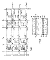
- the active matrix-addressed display device which is suitable for displaying TV pictures, comprises m rows (1 to m) with n horizontally arranged display elements 12 (1 to n) in each row. Only four rows, y to y+3 where m y 1, and a few of the display elements in each row are shown for clarity. In practice, the total number of display elements (mxn) in the matrix array may be 200,000 or more.
- the display elements are referenced LCy,x where y and x designate their row and column positions respectively.
- the display elements are addressed via sets of row and column conductors, here referenced R and C, which extend in spaces between the display elements. For redundancy purposes all rows of the display elements except the first are associated with two row conductors.
- all display elements apart from those in column n are associated with two column conductors.
- the application of data (video) signals to each of these display elements is controlled by switching elements in the form of transistors, designated TAy,x and TBy,x, connected to respective ones of the pairs of row and column conductors associated with the display element.
- the display elements of the first row and of the last column being associated only with a single row conductor and, a single column conductor respectively are, accordingly, associated with a single switching transistor.
- the switching transistors associated with the display elements of each individual row are connected to a respective common pair of row conductors.
- the switching transistors associated with all the display elements in the same column are connected to the same respective common pair of column conductors.
- the switching transistors in this embodiment comprise TFTs fabricated in conventional manner using amorphous silicon or polysilicon technology. The gate and source terminals of the TFTs are connected to their associated row and column conductors respectively.
- a typical display element 12 comprises a transparent drive electrode 14, (shown as a simple square in Figure 1), which is carried on a transparent substrate 10 of the display device together with the row and column conductors and the TFTs and which is connected to the drain terminals of its associated two switching transistors, and an opposing transparent electrode 15 carried on a second, spaced, transparent substrate 16 with liquid crystal material 17 disposed therebetween.
- the opposing electrodes of the display elements on the second substrate comprise individual portions of a common counter electrode coextensive with the area occupied by the drive electrodes in the usual way.
- the two substrates which may be of glass, are provided with polarising layers 18 and 19 and orientation layers 20 and 21 in conventional manner.
- the liquid crystal material serves to modulate light transmitted through the display elements according to a data voltage applied thereto with ear display element being operable to vary light transmission individually through the device in accordance with the voltage applied across its respective electrodes.
- each display element is registered with a colour filter 22 in known manner with groups of three adjacent display elements each providing a colour triplet.
- the triplets are arranged such that diagonally adjacent display elements in the array display the same primary colour, either red, green or blue.
- each display element is further associated with a storage capacitor which in effect is connected to its drive electrode.
- Each of the row conductors R is formed together with an extension constituting a supplementary conductor, generally referenced RS, during its fabrication on the substrate 10 by deposition and definition techniques.
- Each of these supplementary conductors extends as a strip electrode parallel to, and displaced a predetermined distance from, the row conductor and has a respective bridging portion 30 connecting the strip electrode to the row conductor at one end.
- the supplementary conductor RS is spaced from the row conductor R by a distance greater than the distance between two consecutive row conductors but less than the distance between three consecutive row conductors so that, in relation to the subsequently formed drive electrodes of the display elements, it extends beneath the drive electrodes of the next row of display elements in the series to be addressed following those rows of elements with which that row conductor R is associated.
- each supplementary conductor lies under the next but one row of drive electrodes from its interconnected row conductor.
- the supplementary conductors are positioned approximately mid-way across the overlying drive electrodes.
- bridging portions 30 and row conductors cross one another, groups of these portions and the row conductors are fabricated in successive stages with separating insulator material deposited at the appropriate regions, as will be apparent to persons skilled in the art.
- the supplementary conductors RS are separated from their respective rows of drive electrodes 14 by an intervening transparent insulating layer, shown at 23 in Figure 3, acting as dielectric. Overlying portions of the supplementary conductors and drive electrodes overlying one another thus constitute capacitors which are effectively connected at their one side to a drive electrode at their other side to the preceding but one row conductor.
- the display elements are driven on a row at a time basis by scanning the row conductors R sequentially with a switching signal starting from the uppermost row downwards so as to turn on the switching transistors in each row in turn and by applying data signals to the column conductors as appropriate and in synchronism with the switching signals so as to build up a complete display picture.
- the data signals comprise video information signals and each row of display elements is provided with video information signals corresponding to a TV line.
- each of the groups of switching transistors TAy,x and TBy,x associated with a single row of display elements is switched on for a time period Tl during which video information signals are transferred from the column conductors related to those transistors to the display elements and their storage capacitors.
- Tf being approximately equal to m.Tl
- the transistors are turned off and serve to isolate the display elements, and the storage capacitors, from the column conductors.
- each row of display elements is addressed by scanning two consecutive row conductors for redundancy purposes.
- a switching signal Von applied to the row conductor Ry serves to turn on the transistors TAy+1, 1 to TAy+1, n-1 allowing the video information signals then appearing on the column conductors C2 to Cn to be supplied to the display elements LCy+1, 1 to LCy+1, n-1 respectively and their associated storage capacitors.
- the row conductor Ry is connected also to the switching transistors (TBy,1 to TBy,n) for the preceding row of display elements (LCy,1 to LCy,n) these elements and their storage capacitors are similarly supplied with the corresponding video information voltages.
- the switching signal Von is removed from the row conductor Ry and a reference voltage signal V off applied which turns off the transistors TAy+1,1 to TAy+1,n-1 (and likewise the transistors TBy,1 to TBy,n) thereby isolating the storage capacitors for the display elements LCy+1,1 to LCy+1,n-1 (and LCy,1 to LCy,n respectively).
- the switching signal Von is applied to row conductor Ry+1 so as to turn on the transistors TBy+1,1 to TBy+1,n thereby allowing the video information signals now present on the column conductors C1 to Cn to be supplied to the storage capacitors for the display elements LCy+1,1 to LCy+1,n respectively.
- the previously loaded video information of the elements is thus overwritten with the values properly intended for these elements.
- the switching signal Von applied to row conductor Ry+1 also causes the transistors TAy+2,1 to TAy+2, n-1 of the succeeding display element row to be turned on so that the same video information signals on column conductors C2 to C n are supplied also to the storage capacitors of elements LCy+2,1 to LCy+2, n-1 respectively.
- the transistors TBy+1 to TBy+1,n are turned off to isolate the display elements LCy+1,1 to LCy+1,n and their associated storage capacitors so that the last applied video information signals are retained and, in conjunction with a reference voltage applied to the opposing electrodes of the elements, the desired display effect achieved from the elements.
- the display element affected will in these circumstances therefore produce a display effect which is the same as that provided by a diagonally adjacent display element of the preceding row.
- the affected display element will in operation produce the same display effect as its closest display element of the same colour. If a transistor fails closed circuit it can be disconnected by laser scribing or the like thus effectively producing an open circuit type failure.
- the row conductors R are scanned in turn so that the above-described driving scheme is repeated for each row of display elements in turn, the display effect produced by the elements being maintained until they are next addressed in a subsequent field period.
- the display elements of the first row and the last column are each controlled through only one transistor connected to a single row and a single column conductor. Should one of these transistors be defective, complete failure of the individual element of the entire row or column might occur. However, this possibility is not critical as the elements concerned are at the periphery of the display area and would normally be masked from view anyway.
- the first row of display elements are also each associated with two switching transistors. This is achieved by providing an additional row conductor so that the number of row conductors exceeds the number of rows of display elements by one.
- the drive signals applied to the row and column conductors are generated in conventional manner using any suitable known form of drive circuits.
- the supplementary conductors RS are each further connected to their respective row conductors at their other ends through additional bridge portions 31. This provides redundancy in the event of row conductor discontinuities. If a break is present in a row conductor along its length, switching signals can nevertheless be supplied to transistors beyond the discontinuity via the supplementary conductor and the bridge 31. Similarly, in the event of a discontinuity in the supplementary conductor, operation of the storage capacitors beyond the dis continuity is maintained by supply of the voltage Voff from the row conductor via the bridge 31.
- the row and column conductors, supplementary conductors, bridging portions switching transistors and display elements can be fabricated using any suitable conventional technology, as will be apparent to persons skilled in the art.
Landscapes
- Physics & Mathematics (AREA)
- Nonlinear Science (AREA)
- Engineering & Computer Science (AREA)
- Crystallography & Structural Chemistry (AREA)
- Mathematical Physics (AREA)
- Chemical & Material Sciences (AREA)
- Microelectronics & Electronic Packaging (AREA)
- Power Engineering (AREA)
- General Physics & Mathematics (AREA)
- Optics & Photonics (AREA)
- Liquid Crystal (AREA)
- Liquid Crystal Display Device Control (AREA)
- Control Of Indicators Other Than Cathode Ray Tubes (AREA)
- Devices For Indicating Variable Information By Combining Individual Elements (AREA)
Applications Claiming Priority (2)
| Application Number | Priority Date | Filing Date | Title |
|---|---|---|---|
| GB8901037 | 1989-01-18 | ||
| GB8901037A GB2227349A (en) | 1989-01-18 | 1989-01-18 | Display devices |
Publications (3)
| Publication Number | Publication Date |
|---|---|
| EP0379249A2 true EP0379249A2 (de) | 1990-07-25 |
| EP0379249A3 EP0379249A3 (de) | 1991-07-24 |
| EP0379249B1 EP0379249B1 (de) | 1994-12-21 |
Family
ID=10650196
Family Applications (1)
| Application Number | Title | Priority Date | Filing Date |
|---|---|---|---|
| EP90200087A Expired - Lifetime EP0379249B1 (de) | 1989-01-18 | 1990-01-12 | Anzeigevorrichtungen mit aktiver Matrix-Adressierung |
Country Status (5)
| Country | Link |
|---|---|
| US (1) | US5132677A (de) |
| EP (1) | EP0379249B1 (de) |
| JP (1) | JPH02244127A (de) |
| DE (1) | DE69015214T2 (de) |
| GB (1) | GB2227349A (de) |
Families Citing this family (19)
| Publication number | Priority date | Publication date | Assignee | Title |
|---|---|---|---|---|
| KR940008180B1 (ko) * | 1990-12-27 | 1994-09-07 | 가부시끼가이샤 한도다이 에네르기 겐꾸쇼 | 액정 전기 광학 장치 및 그 구동 방법 |
| JP3556679B2 (ja) | 1992-05-29 | 2004-08-18 | 株式会社半導体エネルギー研究所 | 電気光学装置 |
| KR960004150B1 (ko) * | 1991-02-16 | 1996-03-27 | 가부시끼가이샤 한도다이 에네르기 겐꾸쇼 | 표시장치 |
| US6028333A (en) * | 1991-02-16 | 2000-02-22 | Semiconductor Energy Laboratory Co., Ltd. | Electric device, matrix device, electro-optical display device, and semiconductor memory having thin-film transistors |
| EP0536964B1 (de) * | 1991-10-05 | 1998-03-18 | Fujitsu Limited | Aktive Flüssigkristall-Matrix-Anzeige mit verminderter Anzahl von Datenbusleitungen |
| NL194848C (nl) * | 1992-06-01 | 2003-04-03 | Samsung Electronics Co Ltd | Vloeibaar-kristalindicatorinrichting. |
| RU2042973C1 (ru) * | 1992-12-30 | 1995-08-27 | Малое научно-производственное предприятие "ЭЛО" | Жидкокристаллическая цветная дисплейная панель с активной матрицей |
| US5555001A (en) * | 1994-03-08 | 1996-09-10 | Prime View Hk Limited | Redundant scheme for LCD display with integrated data driving circuit |
| JP3402400B2 (ja) | 1994-04-22 | 2003-05-06 | 株式会社半導体エネルギー研究所 | 半導体集積回路の作製方法 |
| US6747627B1 (en) | 1994-04-22 | 2004-06-08 | Semiconductor Energy Laboratory Co., Ltd. | Redundancy shift register circuit for driver circuit in active matrix type liquid crystal display device |
| US5701166A (en) * | 1994-09-26 | 1997-12-23 | Lg Electronics Inc. | Active matrix liquid crystal display having first and second display electrodes capacitively couple to second and first data buses, respectively |
| JP3069280B2 (ja) * | 1995-12-12 | 2000-07-24 | 松下電器産業株式会社 | アクティブマトリックス型液晶表示素子及びその駆動方法 |
| US6518945B1 (en) | 1997-07-25 | 2003-02-11 | Aurora Systems, Inc. | Replacing defective circuit elements by column and row shifting in a flat-panel display |
| GB9807184D0 (en) * | 1998-04-04 | 1998-06-03 | Philips Electronics Nv | Active matrix liquid crystal display devices |
| US6344838B1 (en) * | 1998-04-06 | 2002-02-05 | Em Microelectronic-Marlin Sa | Control device for a liquid crystal display cell |
| JP3906090B2 (ja) * | 2002-02-05 | 2007-04-18 | シャープ株式会社 | 液晶表示装置 |
| KR100482160B1 (ko) * | 2002-09-04 | 2005-04-13 | 엘지.필립스 엘시디 주식회사 | 액정표시장치용 어레이기판 |
| TW200604998A (en) * | 2004-06-23 | 2006-02-01 | Samsung Electronics Co Ltd | Display device |
| US8947297B2 (en) * | 2006-01-30 | 2015-02-03 | The Invention Science Fund I, Llc | Positional display elements |
Family Cites Families (7)
| Publication number | Priority date | Publication date | Assignee | Title |
|---|---|---|---|---|
| US4368523A (en) * | 1979-12-20 | 1983-01-11 | Tokyo Shibaura Denki Kabushiki Kaisha | Liquid crystal display device having redundant pairs of address buses |
| JPS58144888A (ja) * | 1982-02-23 | 1983-08-29 | セイコーインスツルメンツ株式会社 | 行列形液晶表示装置 |
| JPH06100745B2 (ja) * | 1982-07-02 | 1994-12-12 | セイコーエプソン株式会社 | アクティブマトリクス型液晶表示装置 |
| FR2585167B1 (fr) * | 1985-07-19 | 1993-05-07 | Gen Electric | Structures conductrices redondantes pour affichages a cristaux liquides commandes par des transistors a effet de champ en couche mince |
| US4822142A (en) * | 1986-12-23 | 1989-04-18 | Hosiden Electronics Co. Ltd. | Planar display device |
| US4820222A (en) * | 1986-12-31 | 1989-04-11 | Alphasil, Inc. | Method of manufacturing flat panel backplanes including improved testing and yields thereof and displays made thereby |
| EP0283290B1 (de) * | 1987-03-18 | 1994-09-21 | Matsushita Electric Industrial Co., Ltd. | Videoprojektor |
-
1989
- 1989-01-18 GB GB8901037A patent/GB2227349A/en not_active Withdrawn
-
1990
- 1990-01-12 EP EP90200087A patent/EP0379249B1/de not_active Expired - Lifetime
- 1990-01-12 DE DE69015214T patent/DE69015214T2/de not_active Expired - Fee Related
- 1990-01-16 US US07/465,690 patent/US5132677A/en not_active Expired - Fee Related
- 1990-01-18 JP JP2007251A patent/JPH02244127A/ja active Pending
Also Published As
| Publication number | Publication date |
|---|---|
| DE69015214D1 (de) | 1995-02-02 |
| GB8901037D0 (en) | 1989-03-15 |
| DE69015214T2 (de) | 1995-07-20 |
| EP0379249B1 (de) | 1994-12-21 |
| EP0379249A3 (de) | 1991-07-24 |
| US5132677A (en) | 1992-07-21 |
| GB2227349A (en) | 1990-07-25 |
| JPH02244127A (ja) | 1990-09-28 |
Similar Documents
| Publication | Publication Date | Title |
|---|---|---|
| EP0379249B1 (de) | Anzeigevorrichtungen mit aktiver Matrix-Adressierung | |
| EP0297664B1 (de) | Matrix-Anzeigevorrichtungen | |
| US4931787A (en) | Active matrix addressed display system | |
| EP0464579B1 (de) | Dünnfilm-Feldeffekt-Transistormatrix zur Verwendung in Flüssigkristallanzeigen mit aktiver Matrix | |
| US4928095A (en) | Active matrix-addressed picture display device | |
| US5519520A (en) | AC plasma address liquid crystal display | |
| US6037923A (en) | Active matrix display device | |
| JP2578145B2 (ja) | マトリクス表示装置 | |
| JPH0514915B2 (de) | ||
| JPH02134618A (ja) | 表示装置 | |
| US5058995A (en) | Pixel electrode structure for liquid crystal display devices | |
| JP3476885B2 (ja) | 表示装置 | |
| EP0423887A2 (de) | Mit aktiver Matrix adressierte Anzeigevorrichtungen | |
| EP0315365B1 (de) | Anzeigegerät | |
| JPS61228491A (ja) | 表示装置 | |
| JP2517842B2 (ja) | 表示装置 | |
| EP0983530A1 (de) | Elektrooptische Anzeige mit überzähliger Speicherkondensatorstruktur | |
| KR100248199B1 (ko) | 액정표시소자 | |
| EP0406975A2 (de) | Mit aktiver Matrix adressierte Anzeigevorrichtung | |
| JPH0470820A (ja) | アクティブ・マトリックス型平板表示装置 | |
| JPH0854603A (ja) | アクティブマトリックス液晶表示装置 | |
| EP0430487B1 (de) | Matrixadressierbare Anzeigevorrichtungen | |
| US6052102A (en) | Plasma addressed electro-optical display | |
| CN121171187A (zh) | 显示面板的驱动电路、驱动方法和显示装置 | |
| JPH10240169A (ja) | アクティブマトリクス基板及びその駆動方法 |
Legal Events
| Date | Code | Title | Description |
|---|---|---|---|
| PUAI | Public reference made under article 153(3) epc to a published international application that has entered the european phase |
Free format text: ORIGINAL CODE: 0009012 |
|
| AK | Designated contracting states |
Kind code of ref document: A2 Designated state(s): DE FR GB NL |
|
| PUAL | Search report despatched |
Free format text: ORIGINAL CODE: 0009013 |
|
| AK | Designated contracting states |
Kind code of ref document: A3 Designated state(s): DE FR GB NL |
|
| 17P | Request for examination filed |
Effective date: 19920124 |
|
| RAP3 | Party data changed (applicant data changed or rights of an application transferred) |
Owner name: N.V. PHILIPS' GLOEILAMPENFABRIEKEN Owner name: PHILIPS ELECTRONICS UK LIMITED |
|
| 17Q | First examination report despatched |
Effective date: 19930602 |
|
| GRAA | (expected) grant |
Free format text: ORIGINAL CODE: 0009210 |
|
| AK | Designated contracting states |
Kind code of ref document: B1 Designated state(s): DE FR GB NL |
|
| PG25 | Lapsed in a contracting state [announced via postgrant information from national office to epo] |
Ref country code: NL Effective date: 19941221 |
|
| REF | Corresponds to: |
Ref document number: 69015214 Country of ref document: DE Date of ref document: 19950202 |
|
| ET | Fr: translation filed | ||
| NLV1 | Nl: lapsed or annulled due to failure to fulfill the requirements of art. 29p and 29m of the patents act | ||
| REG | Reference to a national code |
Ref country code: FR Ref legal event code: CD |
|
| PLBE | No opposition filed within time limit |
Free format text: ORIGINAL CODE: 0009261 |
|
| STAA | Information on the status of an ep patent application or granted ep patent |
Free format text: STATUS: NO OPPOSITION FILED WITHIN TIME LIMIT |
|
| 26N | No opposition filed | ||
| PGFP | Annual fee paid to national office [announced via postgrant information from national office to epo] |
Ref country code: GB Payment date: 19961224 Year of fee payment: 8 |
|
| PGFP | Annual fee paid to national office [announced via postgrant information from national office to epo] |
Ref country code: FR Payment date: 19970121 Year of fee payment: 8 |
|
| PGFP | Annual fee paid to national office [announced via postgrant information from national office to epo] |
Ref country code: DE Payment date: 19970319 Year of fee payment: 8 |
|
| PG25 | Lapsed in a contracting state [announced via postgrant information from national office to epo] |
Ref country code: GB Free format text: LAPSE BECAUSE OF NON-PAYMENT OF DUE FEES Effective date: 19980112 |
|
| PG25 | Lapsed in a contracting state [announced via postgrant information from national office to epo] |
Ref country code: FR Free format text: THE PATENT HAS BEEN ANNULLED BY A DECISION OF A NATIONAL AUTHORITY Effective date: 19980131 |
|
| GBPC | Gb: european patent ceased through non-payment of renewal fee |
Effective date: 19980112 |
|
| PG25 | Lapsed in a contracting state [announced via postgrant information from national office to epo] |
Ref country code: DE Free format text: LAPSE BECAUSE OF NON-PAYMENT OF DUE FEES Effective date: 19981001 |
|
| REG | Reference to a national code |
Ref country code: FR Ref legal event code: ST |