EP0379320A1 - Circuit de couplage optique - Google Patents
Circuit de couplage optique Download PDFInfo
- Publication number
- EP0379320A1 EP0379320A1 EP90300392A EP90300392A EP0379320A1 EP 0379320 A1 EP0379320 A1 EP 0379320A1 EP 90300392 A EP90300392 A EP 90300392A EP 90300392 A EP90300392 A EP 90300392A EP 0379320 A1 EP0379320 A1 EP 0379320A1
- Authority
- EP
- European Patent Office
- Prior art keywords
- photocoupler
- phototransistor
- current path
- switching transistor
- circuit
- Prior art date
- Legal status (The legal status is an assumption and is not a legal conclusion. Google has not performed a legal analysis and makes no representation as to the accuracy of the status listed.)
- Withdrawn
Links
Images


Classifications
-
- H—ELECTRICITY
- H03—ELECTRONIC CIRCUITRY
- H03K—PULSE TECHNIQUE
- H03K17/00—Electronic switching or gating, i.e. not by contact-making and –breaking
- H03K17/51—Electronic switching or gating, i.e. not by contact-making and –breaking characterised by the components used
- H03K17/78—Electronic switching or gating, i.e. not by contact-making and –breaking characterised by the components used using opto-electronic devices, i.e. light-emitting and photoelectric devices electrically- or optically-coupled
- H03K17/795—Electronic switching or gating, i.e. not by contact-making and –breaking characterised by the components used using opto-electronic devices, i.e. light-emitting and photoelectric devices electrically- or optically-coupled controlling bipolar transistors
- H03K17/7955—Electronic switching or gating, i.e. not by contact-making and –breaking characterised by the components used using opto-electronic devices, i.e. light-emitting and photoelectric devices electrically- or optically-coupled controlling bipolar transistors using phototransistors
Definitions
- the present invention relates to a photocoupler for transmitting, at a high speed, a signal insulated by a photocoupler and particularly to a photocoupler circuit for driving a power semiconductor element which can drive at a high speed said power semiconductor element.
- the ON-OFF signal to be applied to such semiconductor element is insulated and transmitted by photocoupler.
- the power conversion by means of pulse width modulation control is required to form a photocoupler circuit to satisfy the requirement that such ON-OFF signal must be transmitted at high speed.
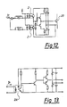
- Fig. 12 is a schematic circuit diagram showing a first prior art form of photocoupler circuit for transmitting a signal.
- a pair of general purpose photocouplers are used to insulate and transmit the ON-OFF signal to a power transistor 20 as a power semiconductor element because a general purpose photocoupler uses a phototransistor to receive the light and the long transition time from ON to OFF of this phototransistor must be shortened.
- the long transition time from ON to OFF of such a phototransistor occurs because of the long time required to eliminate excessive carriers accumulated in the phototransistor.
- Fig. 13 is a circuit diagram of a second prior art form of photocoupler circuit for transmitting a signal.
- a high speed photocoupler 2A is used for insulating and transmitting a signal and instead of a pair of photocouplers as shown in Fig. 12, only a single such photocoupler is provided.
- a photocoupler circuit having a light-emitting element arranged to be driven by means of an input signal and a phototransistor arranged to detect the resulting light signal from the light-emitting element and to produce a current in its main current path as a result of said detection, said photocoupler circuit being characterised in that one side of the main current path of the phototransistor is connected to one side of power supply means via a circuit portion connected in parallel with the current path between the control electrode and one side of the main current path of a switching transistor, the other side of the main current path of the phototransistor being connected to the other side of the power supply means, the voltage across the main current path of the switching transistor being arranged to provide an output signal of the photocoupler circuit.
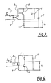
- an input resistance 1 is provided in the input side (having associated input terminals) of a general purpose or low speed photocoupler 2 (hereinafter only referred to as a photocoupler) and the value of the drive current IF of the photocoupler 2 is determined by means of a voltage applied to the input terminals and the value of the input resistance 1.
- a general purpose or low speed photocoupler 2 hereinafter only referred to as a photocoupler
- a phototransistor forming the output side of the photocoupler 2 switches ON.
- This phototransistor has its emitter connected to resistor 3 connected between the base and emitter of an NPN switching transistor 4 and is further connected with a first DC power supply 6.
- V1 the voltage across the base and emitter of the switching transistor 4
- V BE * the voltage across collector and emitter of the phototransistor
- V BE * is set to a value as low as about 0.6 to 0.7 volts
- V CE becomes almost equal to the voltage V1 of the first DC power supply 6 and the phototransistor is biassed in the active region. Accordingly, the switching speed of photocoupler 2 is improved remarkably.
- graph 2(a) represents changes with time in the current I F for driving the photocoupler 2;
- graph 2(b) represents changes with time of output voltage V CE of the photocoupler 2 and
- graph 2(c) changes with time of an output voltage V0 of the entire photocoupler circuit.
- the resistor 3 may be omitted if the carrier dissipation time of the switching transistor 4 is to be very short.
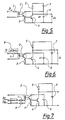
- switching transistor 4A is a PNP transistor and the functions of the input resistor 1, photocoupler 2 and resistors 3 and 5, first DC power supply 6 and second DC power supply 7 are the same as in the first embodiment but with the difference in connection and polarity corresponding to the use of a PNP transistor 4A.
- the photocoupler circuit shown is the same as the first embodiment shown in Fig. 1, except that the first DC power supply 6 is used both for power supply to the phototransistor of the photocoupler 2 and to the switching transistor 4.
- the second DC power supply 7 is thus eliminated.
- the fourth embodiment of photocoupler circuit shown is the same as the first embodiment shown in Fig. 1, except that the first DC power supply 6 is provided for the phototransistor of photocoupler 2, while a series connected arrangement of the first DC power supply 6 and the second DC power supply 7 is provided for the switching transistor 4.
- a photocoupler circuit in a first form of apparatus using a photocoupler circuit the output circuit following the photocoupler 2 is the same as for the first embodiment shown in Fig. 1 but the signal input circuit to the photocoupler 2 is different.
- the input resistor 1 provided in the input side of photocoupler 2 is connected with a differential circuit 8 formed by a resistor and a capacitor to amplify variation in photocoupler drive current I F . Therefore, the signal transmission period for turning ON the photocoupler 2 can be shortened.
- a second form of apparatus using a photocoupler circuit also shortens the signal transmission period for turning ON the photocoupler.
- the apparatus is similar to that shown in Fig. 6 but has a different input circuit arrangement in that drive current I F2 flowing into input resistor 9 is superposed on the drive current I F1 flowing into the input resistor 1 provided in the input side of the photocoupler 2.
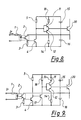
- an input operating signal is supplied to, and isolated by means of, the photocoupler 2 which transmits the signal at high speed in order to turn ON and OFF a semiconductor power element in the form of power transistor 20.
- the common connecting point of the gate and emitter of the switching transistor 4 is connected to the phototransistor of a photocoupler 2 and a reverse-bias power supply 16 of the power transistor 20 is connected in the resulting circuit so that the transistor 20 is normally reverse-biassed until the occurrence of an appropriate input signal.
- reverse-bias power supply 16 and forward-bias power supply 15 is connected between the collector and emitter of the switching transistor 4 and operation of this switching transistor 4 gives rise to a signal at the gates of forward-bias transistor 11 and reverse-bias transistor 12.
- the current transmission ratio of the photocoupler 2 becomes very large because the switching transistor 4 can be driven with only a little current while the photocoupler is operated in the active region. That is, the value of the drive current I F of the photocoupler 2 can be reduced in comparison with the corresponding value in prior art circuits.
- a sixth embodiment of photocoupler circuit is for driving a semiconductor power element and is the same as the fifth embodiment shown in Fig. 8, except that an amplifying transistor 17 is provided as a further stage to the switching transistor 4 to operate the forward-bias transistor 11 and the reverse-bias transistor 12.
- a seventh embodiment of photocoupler circuit for driving a semiconductor power element is the same as the fifth embodiment shown in Fig. 8, except that a PNP transistor is used for the forward-bias transistor 21 and an NPN transistor is used for the reverse-bias transistor 22.
- a series arrangement of resistor 24 and constant voltage (zener) diode 23 is connected to the forward-bias power supply 15 in order to enable the constant voltage diode 23 to provide the function of a reverse-bias power supply so that one DC power supply can be omitted.
- the signal input circuit to the photocoupler 2 is different from that in the fifth embodiment shown in Fig. 8.
- a differential circuit 8 comprising a resistor and a capacitor is connected in parallel with the input resistor 1 provided in the input side of the photocoupler 2 to amplify variation in the photocoupler drive current I F so that the signal transmission time for turning ON the photocoupler 2 can be shortened.
- the system of using two parallel-connected resistors 1 and 9 to increase photocoupler drive current as shown in Fig. 7, or the system of using a differential circuit 8 as shown in Figs. 6 and 11 and a system using a constant voltage diode 23 as shown in Fig. 11 as the DC power supply can be applied as appropriate in any of the other embodiments not employing such systems.
- the photocoupler circuit is so structured that the phototransistor of the photocoupler, the circuit across the base and emitter of the switching transistor and the first DC power supply are connected in series, the photocoupler is used as a current output switch operating in the active region.
- the photocoupler With an output signal being extracted from the collector of the switching transistor, even using a general purpose photocoupler having transmission delay when going to the OFF signal state, the signal can be transmitted at a high speed and it is no longer necessary to use a large and expensive high speed photocoupler.
- a general purpose photocoupler may be used in a power conversion unit which is particularly required to provide high speed operation, resulting in the effect that the entire unit may be reduced in size and can be built at low cost.
- the photocoupler may be used as a current output switch with reduced photocoupler drive because it provides a high current transmission ratio. In this aspect the embodiments described above provide a significant contribution to realisation of small size and low cost.
- the connecting point to the base-emitter junction of the switching transistor is connected in series with the collector and emitter terminals of the phototransistor of the photocoupler and a voltage is applied to this circuit.
Landscapes
- Electronic Switches (AREA)
- Photo Coupler, Interrupter, Optical-To-Optical Conversion Devices (AREA)
Applications Claiming Priority (2)
| Application Number | Priority Date | Filing Date | Title |
|---|---|---|---|
| JP1008312A JPH02188020A (ja) | 1989-01-17 | 1989-01-17 | ホトカプラ回路および電力用半導体素子の駆動用ホトカプラ回路 |
| JP8312/89 | 1989-01-17 |
Publications (1)
| Publication Number | Publication Date |
|---|---|
| EP0379320A1 true EP0379320A1 (fr) | 1990-07-25 |
Family
ID=11689636
Family Applications (1)
| Application Number | Title | Priority Date | Filing Date |
|---|---|---|---|
| EP90300392A Withdrawn EP0379320A1 (fr) | 1989-01-17 | 1990-01-15 | Circuit de couplage optique |
Country Status (3)
| Country | Link |
|---|---|
| US (1) | US5043587A (fr) |
| EP (1) | EP0379320A1 (fr) |
| JP (1) | JPH02188020A (fr) |
Cited By (3)
| Publication number | Priority date | Publication date | Assignee | Title |
|---|---|---|---|---|
| EP1269660B1 (fr) * | 2000-03-31 | 2012-04-18 | Micro Motion, Inc. | Optocoupleur pour circuit a securite non intrinseque |
| CN106464250A (zh) * | 2014-10-08 | 2017-02-22 | 株式会社Lg 化学 | 用于控制隔离开关的设备和方法 |
| CN108111156A (zh) * | 2017-12-29 | 2018-06-01 | 深圳市中航比特通讯技术有限公司 | 一种隔离开关电路 |
Families Citing this family (14)
| Publication number | Priority date | Publication date | Assignee | Title |
|---|---|---|---|---|
| JPH01270117A (ja) * | 1988-04-22 | 1989-10-27 | Fanuc Ltd | 出力回路 |
| US5182448A (en) * | 1990-10-05 | 1993-01-26 | Sharp Kabushiki Kaisha | Photocoupler with improved anti-noise characteristics |
| US5182456A (en) * | 1992-02-25 | 1993-01-26 | The United States Of America As Represented By The Secretary Of The Navy | Noise attenuating circuit for mechanical relay including optical isolation |
| US5189307A (en) * | 1992-03-13 | 1993-02-23 | Empi, Inc. | Isolated current mirror with optical insulator generating feedback signal |
| US5434694A (en) * | 1992-03-31 | 1995-07-18 | Yokogawa Electric Corporation | Signal isolating device |
| US5221847A (en) * | 1992-06-26 | 1993-06-22 | At&T Bell Laboratories | Break-before-make control for form C solid-state relays with current limiter bypass |
| US6531925B2 (en) * | 2001-07-17 | 2003-03-11 | David C. Scott | Heterojunction bipolar transistor optoelectronic transimpedance amplifier using the first transistor as an optical detector |
| CN2690894Y (zh) * | 2004-03-09 | 2005-04-06 | 鸿富锦精密工业(深圳)有限公司 | 风扇马达检测电路 |
| US7764479B2 (en) * | 2007-04-18 | 2010-07-27 | Lutron Electronics Co., Inc. | Communication circuit for a digital electronic dimming ballast |
| US7808759B2 (en) * | 2007-06-21 | 2010-10-05 | Avago Technologies Ecbu Ip (Singapore) Pte. Ltd. | Methods and apparatuses for performing common mode pulse compensation in an opto-isolator |
| US8116055B2 (en) * | 2007-06-21 | 2012-02-14 | Avago Technologies Ecbu Ip (Singapore) Pte. Ltd. | Methods and apparatuses for performing common mode pulse compensation in an opto-isolator |
| CN104038203B (zh) * | 2013-03-06 | 2017-04-05 | 欣旺达电子股份有限公司 | 光耦通信加速系统 |
| CN103743481B (zh) * | 2014-02-20 | 2017-03-15 | 三维通信股份有限公司 | 一种极低成本检测范围可调的光强检测电路 |
| WO2023275339A1 (fr) * | 2021-06-30 | 2023-01-05 | Grundfos Holding A/S | Circuit opto-coupleur haute vitesse |
Citations (8)
| Publication number | Priority date | Publication date | Assignee | Title |
|---|---|---|---|---|
| DE2163495A1 (de) * | 1971-12-21 | 1973-07-05 | Gehap Gmbh & Co Kg | Opto-gekoppeltes elektronisches relais mit galvanischer trennung von steuerkreis und schaltkreis |
| DE2344891A1 (de) * | 1973-09-06 | 1975-03-20 | Wolfgang Hoffmann | Elektronisches relais |
| DE2253423B2 (de) * | 1971-11-01 | 1976-03-18 | International Rectifier Corp., Los Angeles, Calif. (V.St.A.) | Festkoerper-relaisschaltung |
| US4021683A (en) * | 1975-01-03 | 1977-05-03 | National Research Development Corporation | Electronic switching circuits |
| US4137428A (en) * | 1977-10-27 | 1979-01-30 | Bell Telephone Laboratories, Incorporated | Optically actuated bidirectional semiconductor switch |
| DE2930176A1 (de) * | 1978-08-30 | 1980-03-13 | Texas Instruments Inc | Mikroelektronische halbleiterschalteranordnung und damit ausgestattete optoelektronische steueranordnung |
| US4355237A (en) * | 1980-08-04 | 1982-10-19 | Texas Instruments Incorporated | High speed AC/DC coupler |
| US4369371A (en) * | 1980-11-24 | 1983-01-18 | Canadian Patents & Dev. Limited | Broadband high speed optoelectronic semiconductor switch |
Family Cites Families (6)
| Publication number | Priority date | Publication date | Assignee | Title |
|---|---|---|---|---|
| US3767978A (en) * | 1972-03-17 | 1973-10-23 | A Wernli | Voltage-isolating, keying arrangement for a power-line carrier system |
| US3902060A (en) * | 1972-04-04 | 1975-08-26 | Westinghouse Electric Corp | Self-optimizing biasing feedback for photo-electric transmission systems |
| US4027228A (en) * | 1975-04-15 | 1977-05-31 | General Electric Company | Photocoupled isolated switching amplifier circuit |
| US4143187A (en) * | 1977-12-01 | 1979-03-06 | Du Pont Of Canada Limited | Process for coating sheet substrates with thermoplastic polymer |
| JPS57197932A (en) * | 1981-05-29 | 1982-12-04 | Hitachi Ltd | Signal transmitting circuit |
| JPS5894218A (ja) * | 1981-11-30 | 1983-06-04 | Semiconductor Res Found | フオトカツプラ |
-
1989
- 1989-01-17 JP JP1008312A patent/JPH02188020A/ja active Pending
-
1990
- 1990-01-15 EP EP90300392A patent/EP0379320A1/fr not_active Withdrawn
- 1990-01-17 US US07/466,492 patent/US5043587A/en not_active Expired - Fee Related
Patent Citations (8)
| Publication number | Priority date | Publication date | Assignee | Title |
|---|---|---|---|---|
| DE2253423B2 (de) * | 1971-11-01 | 1976-03-18 | International Rectifier Corp., Los Angeles, Calif. (V.St.A.) | Festkoerper-relaisschaltung |
| DE2163495A1 (de) * | 1971-12-21 | 1973-07-05 | Gehap Gmbh & Co Kg | Opto-gekoppeltes elektronisches relais mit galvanischer trennung von steuerkreis und schaltkreis |
| DE2344891A1 (de) * | 1973-09-06 | 1975-03-20 | Wolfgang Hoffmann | Elektronisches relais |
| US4021683A (en) * | 1975-01-03 | 1977-05-03 | National Research Development Corporation | Electronic switching circuits |
| US4137428A (en) * | 1977-10-27 | 1979-01-30 | Bell Telephone Laboratories, Incorporated | Optically actuated bidirectional semiconductor switch |
| DE2930176A1 (de) * | 1978-08-30 | 1980-03-13 | Texas Instruments Inc | Mikroelektronische halbleiterschalteranordnung und damit ausgestattete optoelektronische steueranordnung |
| US4355237A (en) * | 1980-08-04 | 1982-10-19 | Texas Instruments Incorporated | High speed AC/DC coupler |
| US4369371A (en) * | 1980-11-24 | 1983-01-18 | Canadian Patents & Dev. Limited | Broadband high speed optoelectronic semiconductor switch |
Cited By (6)
| Publication number | Priority date | Publication date | Assignee | Title |
|---|---|---|---|---|
| EP1269660B1 (fr) * | 2000-03-31 | 2012-04-18 | Micro Motion, Inc. | Optocoupleur pour circuit a securite non intrinseque |
| CN106464250A (zh) * | 2014-10-08 | 2017-02-22 | 株式会社Lg 化学 | 用于控制隔离开关的设备和方法 |
| EP3118997A4 (fr) * | 2014-10-08 | 2017-11-08 | LG Chem, Ltd. | Dispositif et procédé de commande d'un commutateur d'isolation |
| CN106464250B (zh) * | 2014-10-08 | 2019-06-18 | 株式会社Lg 化学 | 用于控制隔离开关的设备和方法 |
| CN108111156A (zh) * | 2017-12-29 | 2018-06-01 | 深圳市中航比特通讯技术有限公司 | 一种隔离开关电路 |
| CN108111156B (zh) * | 2017-12-29 | 2018-11-30 | 深圳市中航比特通讯技术有限公司 | 一种隔离开关电路 |
Also Published As
| Publication number | Publication date |
|---|---|
| JPH02188020A (ja) | 1990-07-24 |
| US5043587A (en) | 1991-08-27 |
Similar Documents
| Publication | Publication Date | Title |
|---|---|---|
| EP0379320A1 (fr) | Circuit de couplage optique | |
| KR930001442B1 (ko) | 반도체 릴레이 회로 | |
| US4721869A (en) | Protection circuit for an insulated gate bipolar transistor utilizing a two-step turn off | |
| KR900004074A (ko) | 절연된 게이트 트랜지스터, 절연된 게이트 트랜지스터를 갖는 스위칭회로, 절연된 게이트트랜지스터를 갖는 유도전동기 시스템, 과전류검출방법 그리고 절연게이트트랜지스터를 위한 회로를 위한 드라이브회로와 반도체장치 | |
| GB2112598A (en) | Control circuit for switching inductive loads | |
| US4695915A (en) | Short circuit and overload protection circuit for output stage transistors | |
| EP0921624B1 (fr) | Dispositif de commande d'un element de puissance de type a auto-extinction d'arc | |
| KR0164638B1 (ko) | 광 결합기 장치 | |
| EP0181201B1 (fr) | Circuit d'attaque pour un transistor Darlington de puissance bipolaire | |
| USRE34107E (en) | Power transistor drive circuit with improved short circuit protection | |
| US5965961A (en) | Electrical circuit arrangement | |
| US5075568A (en) | Switching bipolar driver circuit for inductive load | |
| US5027020A (en) | Zero voltage switching AC relay circuit | |
| US4114054A (en) | Coupling circuit using a photocoupler | |
| US4568838A (en) | Control circuit for a semiconductor element with a control electrode | |
| US4220873A (en) | Temperature compensated switching circuit | |
| KR900002597B1 (ko) | 트랜지스터 인버터의 베이스 드라이브 회로 | |
| US4221980A (en) | Electrical switching means | |
| US5170059A (en) | Optically coupled fast turn off load switch drive | |
| JPH06244694A (ja) | 半導体スイッチ装置 | |
| US3165640A (en) | D. c. controlled semiconductor switch for a. c. current | |
| CN222191841U (zh) | 一种负载驱动电路 | |
| KR100354726B1 (ko) | 집적형 전력 증폭단을 제어하기 위한 방법 및 장치 | |
| US3307082A (en) | Switching arrangement | |
| KR100246553B1 (ko) | 디지탈 회로용 출력단 |
Legal Events
| Date | Code | Title | Description |
|---|---|---|---|
| PUAI | Public reference made under article 153(3) epc to a published international application that has entered the european phase |
Free format text: ORIGINAL CODE: 0009012 |
|
| 17P | Request for examination filed |
Effective date: 19900202 |
|
| AK | Designated contracting states |
Kind code of ref document: A1 Designated state(s): DE FR GB |
|
| 17Q | First examination report despatched |
Effective date: 19920514 |
|
| STAA | Information on the status of an ep patent application or granted ep patent |
Free format text: STATUS: THE APPLICATION IS DEEMED TO BE WITHDRAWN |
|
| 18D | Application deemed to be withdrawn |
Effective date: 19930206 |