EP0379640A2 - Übertragungssystem für Funksende- und -empfangsgerät - Google Patents
Übertragungssystem für Funksende- und -empfangsgerät Download PDFInfo
- Publication number
- EP0379640A2 EP0379640A2 EP19890116524 EP89116524A EP0379640A2 EP 0379640 A2 EP0379640 A2 EP 0379640A2 EP 19890116524 EP19890116524 EP 19890116524 EP 89116524 A EP89116524 A EP 89116524A EP 0379640 A2 EP0379640 A2 EP 0379640A2
- Authority
- EP
- European Patent Office
- Prior art keywords
- data
- transmission system
- control block
- microcomputer control
- transmission
- Prior art date
- Legal status (The legal status is an assumption and is not a legal conclusion. Google has not performed a legal analysis and makes no representation as to the accuracy of the status listed.)
- Granted
Links
Images
Classifications
-
- H—ELECTRICITY
- H04—ELECTRIC COMMUNICATION TECHNIQUE
- H04L—TRANSMISSION OF DIGITAL INFORMATION, e.g. TELEGRAPHIC COMMUNICATION
- H04L25/00—Baseband systems
- H04L25/02—Details ; arrangements for supplying electrical power along data transmission lines
- H04L25/0264—Arrangements for coupling to transmission lines
- H04L25/028—Arrangements specific to the transmitter end
- H04L25/0286—Provision of wave shaping within the driver
-
- H—ELECTRICITY
- H04—ELECTRIC COMMUNICATION TECHNIQUE
- H04B—TRANSMISSION
- H04B1/00—Details of transmission systems, not covered by a single one of groups H04B3/00 - H04B13/00; Details of transmission systems not characterised by the medium used for transmission
- H04B1/38—Transceivers, i.e. devices in which transmitter and receiver form a structural unit and in which at least one part is used for functions of transmitting and receiving
-
- H—ELECTRICITY
- H04—ELECTRIC COMMUNICATION TECHNIQUE
- H04L—TRANSMISSION OF DIGITAL INFORMATION, e.g. TELEGRAPHIC COMMUNICATION
- H04L25/00—Baseband systems
- H04L25/02—Details ; arrangements for supplying electrical power along data transmission lines
- H04L25/0264—Arrangements for coupling to transmission lines
- H04L25/0292—Arrangements specific to the receiver end
-
- H—ELECTRICITY
- H04—ELECTRIC COMMUNICATION TECHNIQUE
- H04W—WIRELESS COMMUNICATION NETWORKS
- H04W88/00—Devices specially adapted for wireless communication networks, e.g. terminals, base stations or access point devices
- H04W88/02—Terminal devices
Definitions
- the invention is based on a transmission system according to the preamble of claim 1.
- Such a transmission system is known (BOSCH technical information, mobile radio systems KF mini-S (KF 83/163/453), imprint: EK-VKD 8 699 920 919 (08410) F), in which between a radio transmitter and receiver and an associated mobile control unit, a multi-core cable is provided, via which voice signals and possibly also control signals can be transmitted in both directions.
- this system does not allow the number of connecting wires to be reduced; in addition, it is not possible to connect additional control units to the radio transmitters and receivers.
- the invention has for its object to develop a transmission system according to the preamble of claim 1 such that a minimum number of lines is required for the bidirectional transmission of digital and analog signals that emit only a little interference radiation to the outside and by interference radiation from the outside can hardly be influenced. Furthermore, the transmission system should be expandable with regard to additional peripheral devices, without the number of line connections required thereby increasing significantly.
- a preferred field of application for the invention is a radio telephone system in which the line connection between the transceiver block of the radio transceiver and peripheral input and output components is provided and in which the voice is transmitted analog or digital and the data digital.
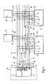
- the radio transceiver 10 comprises a radio transceiver 10, which is preferably a radio telephone, with a microcomputer control block 11 and an analog signal processing circuit 12. With the microcomputer control block and the signal processing circuit are a first via lines 13 Operating unit 14, a data terminal 15, a card reader 16 and a second operating unit 17 are connected.
- the signal conditioning circuit 12 has a microphone connection 20, a receiver connection 21 and a ground connection 22 and the microcomputer control block 11 an operating voltage connection 23, a further ground connection 24, a data connection 25, a control line connection 26 and a switching line connection 27.
- the microphone connection 20 and the receiver connection 21 are connected via a first shielded line 30 to a microphone connection 31 and a receiver connection 32 of the first and second operating parts 14, 17.
- the shielding of the first shielded line 30 is connected to the ground connection 22 of the signal processing circuit 12 and to a ground connection 33 of the first and second operating parts 14, 17.
- the data connection 25 and the control line connection 26 are connected via a second shielded line 35 to a data connection 36 and a control line connection 37 of the first and second operating parts 14, 17.
- the shielding of the second shielded line 35 is connected to the further ground connection 24 of the microcomputer control block 11 and to ground connections 38 of the first and second operating parts 14, 17.
- the operating voltage connection 23 of the microcomputer control block 11 is connected via an operating potential line 40 to operating voltage connections 41 and the switching line connection 27 via a switching line 42 to switching line connections 43 of the operating parts 14 and 17.
- the data connection 25 and the further ground connection 24 are also connected via the second shielded line 35 to a data connection 45, a ground connection 46 and the operating voltage connection 23 via line 40 to an operating voltage connection 47 of the data terminal 15 and the card reader 16.
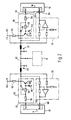
- an active pulse filter 55, 56 is in each case at the data outputs 50, 51 of the ports 52, 53 of the microcomputer control blocks 11, 18 (TxD) of the radio transmitter and receiver device 10 and of the control unit 14 and, if appropriate, further peripheral devices 19 connected.
- the active pulse filters each contain two resistors 59, 60 located in series between the data output 50 and 51 and the base of a transistor 58. From the connection point between the two resistors 59, 60, a connection leads via a first capacitor 61 to the emitter of the transistor 58. A second capacitor 62 connects the base of transistor 58 to ground potential.
- the emitters of the transistors 58 are each connected via a pull-up resistor 63, 64 to a terminal 65 of positive potential of 5 V, for example.
- a passive pulse filter 66, 67 connects to the emitters of the transistors 58 and to the outputs of the active pulse filters 55, 56, which is preferably an LC filter.
- the pulse filters 55, 56, 66, 67 have the purpose of smoothing the edges of the data signals to be fed into the data signal line 57 and thus reducing their edge steepness.
- the active pulse filters 55, 56 have, for example, a cutoff frequency of about 5 kHz and the passive pulse filters 66, 67 have a cutoff frequency of about 100 kHz.
- each data input 68, 69 RxD
- a threshold switch 70, 71 in front of each data input 68, 69 (RxD), which is preferably a Schmitt trigger with a structure familiar to the person skilled in the art.
- the ports 52, 53 of the radio transceiver 10 and the control unit 14 and the ports of further peripheral devices 19 each belong to a serial interface, the interface of which preferably corresponds to the RS 232 C or V24 standard.
- the signal transmission is preferably asynchronous in NRZ (no return to zero) format.
- a cyclic redundancy check method for example, is suitable as a data backup method for data transmission.
- the data are transferred in blocks in series and starting with the least significant bit.
- the mode of operation of the circuit arrangement according to FIG. 2 is as follows.
- the edges of the individual bits are ground off by means of the active pulse filter 55 and the passive pulse filter 66 and transmitted via the data line 57 to the data input 69 of the control unit 14.
- the threshold switch 71 In front of the data input 69 is the threshold switch 71, which forms square-wave pulses from the data signals having ground edges.
- the pull-up resistors 63 and 64 have the effect that any number of peripheral devices can be connected to the data line 57.
Landscapes
- Engineering & Computer Science (AREA)
- Computer Networks & Wireless Communication (AREA)
- Signal Processing (AREA)
- Power Engineering (AREA)
- Transceivers (AREA)
- Pharmaceuticals Containing Other Organic And Inorganic Compounds (AREA)
- Liquid Crystal Substances (AREA)
- Bidirectional Digital Transmission (AREA)
- Noise Elimination (AREA)
- Selective Calling Equipment (AREA)
- Vehicle Body Suspensions (AREA)
- Radio Transmission System (AREA)
- Reduction Or Emphasis Of Bandwidth Of Signals (AREA)
- Radar Systems Or Details Thereof (AREA)
- Burglar Alarm Systems (AREA)
Abstract
Description
- Die Erfindung geht von einem Übertragungssystem nach dem Oberbegriff des Anspruchs 1 aus.
- Es ist ein derartiges Übertragungssystem bekannt (BOSCH Technische Informationen, Mobile Sprechfunkanlagen KF mini-S (KF 83/163/453), Impressum: EK-VKD 8 699 920 919 (08410) F), bei dem zwischen einem Funksende- und -empfangsgerät und einem zugehörigen mobilen Bedienteil ein vieladriges Kabel vorgesehen ist, über das Sprachsignale und gegebenenfalls auch Steuersignale in beiden Richtungen übertragen werden können. Dieses System gestattet jedoch keine Reduzierung der Zahl der Verbindungsadern; außerdem ist keine Anschaltung weiterer Bedienteile an das Funksende- und -empfangsgeräte möglich.
- Der Erfindung liegt die Aufgabe zugrunde, ein Übertragungssystem nach dem Oberbegriff des Anspruchs 1 derart weiterzubilden, daß für die bidirektionale Übertragung von digitalen und analogen Signalen eine minimale Zahl von Leitungen erforderlich ist, die nur eine geringe Störstrahlung nach außen abgeben und durch eine Störstrahlung von außen kaum beeinflußt werden. Weiterhin soll das Übertragungssystem im Hinblick auf zusätzliche periphere Geräte erweiterbar sein, ohne daß sich dadurch die Zahl der erforderlichen Leitungsverbindungen wesentlich erhöht.
- Diese Aufgabe wird bei einem Übertragungssystem nach dem Oberbegriff des Anspruchs 1 durch die kennzeichnenden Merkmale dieses Anspruchs gelöst. Die mit der Erfindung erzielbaren Vorteile bestehen insbesondere darin, daß im günstigsten Fall nur eine zwei Leiter umfassende Leitung zwischen einem Funksende- und -empfangsgerät und einem peripheren Gerät erforderlich ist, die störstrahlungsarm und störeinstrahlungsunanfällig ist. An die eine Leitung können weitere periphere Geräte angeschlossen werden, ohne daß sich dadurch eine Verschlechterung hinsichtlich der Störstrahlungsaussendung bzw. Störeinstrahlung ergibt.
- Ein bevorzugtes Anwendungsgebiet für die Erfindung ist ein Funktelefonsystem, bei dem die Leitungsverbindung zwischen dem Sende-Empfangsblock des Funksende- und -empfangsgerätes und peripheren Ein- und Ausgabekomponenten vorgesehen ist und bei dem die Sprache analog oder digital und die Daten digital übertragen werden.
- Ausführungsbeispiele der Erfindung sind in der Zeichnung an Hand zweier Figuren dargestellt und werden im folgenden näher beschrieben. Es zeigen
- Fig. 1 ein Blockschaltbild eines Funksende- und -empfangsgerätes mit über Busleitungen angeschlossenen Bedienteilen, einem Kartenleser und einem Display und
- Fig. 2 ein ausführlicheres Blockschaltbild zu Fig. 1 mit einem Funksende- und -empfangsgerät und einem Bedienteil.
- Ein Übertragungssysstem gemäß dem Blockschaltbild nach Fig. 1 umfaßt ein Funksende- und -empfangsgerät 10, das ist vorzugsweise ein Funktelefon, mit einem Mikrocomputer-Steuerblock 11 und einer analogen Signalaufbereitungsschaltung 12. Mit dem Mikrocomputer-Steuerblock und der Signalaufbereitungsschaltung sind über Leitungen 13 ein erstes Bedienteil 14, ein Datenterminal 15, ein Kartenleser 16 und ein zweites Bedienteil 17 verbunden. Die Signalaufbereitungsschaltung 12 hat einen Mikrofonanschluß 20, einen Höreranschluß 21 und einen Masseanschluß 22 und der Mikrocomputer-Steuerblock 11 einen Betriebsspannungsanschluß 23, einen weiteren Masseanschluß 24, einen Datenanschluß 25, einen Steuerleitungsanschluß 26 und einen Schaltleitungsanschluß 27.
- Der Mikrofonanschluß 20 und der Höreranschluß 21 sind über eine erste abgeschirmte Leitung 30 mit einem Mikrofonanschluß 31 und einem Höreranschluß 32 des ersten und zweiten Bedienteils 14, 17 verbunden. Die Abschirmung der ersten abgeschirmten Leitung 30 ist mit dem Masseanschluß 22 der Signalaufbereitungsschaltung 12 und mit je einem Masseanschluß 33 des ersten und zweiten Bedienteils 14, 17 verbunden.
- Der Datenanschluß 25 und der Steuerleitungsanschluß 26 sind über eine zweite abgeschirmte Leitung 35 mit einem Datenanschluß 36 und einem Steuerleitungsanschluß 37 des ersten und zweiten Bedienteils 14, 17 verbunden. Die Abschirmung der zweiten abgeschirmten Leitung 35 ist mit dem weiteren Masseanschluß 24 des Mikrocomputer-Steuerblocks 11 sowie mit Masseanschlüssen 38 des ersten und zweiten Bedienteils 14, 17 verbunden.
- Der Betriebsspannungsanschluß 23 des Mikrocomputer-Steuerblocks 11 steht über eine Betriebspotentialleitung 40 mit Betriebsspannungsanschlüssen 41 und der Schaltleitungsanschluß 27 über eine Schaltleitung 42 mit Schaltleitungsanschlüssen 43 der Bedienteile 14 und 17 in Verbindung. Der Datenanschluß 25 und der weitere Masseanschluß 24 stehen außerdem über die zweite abgeschirmte Leitung 35 noch mit je einem Datenanschluß 45, je einem Masseanschluß 46 und der Betriebsspannungsanschluß 23 über die Leitung 40 mit je einem Betriebsspannungsanschluß 47 des Datenterminals 15 und des Kartenlesers 16 in Verbindung.
- Für die Sprachsignal-, Datensignal-, Steuersignal- und Schaltsignalübertragung zwischen dem Funksende- und -empfangsgerät 10 und den Bedienteilen 14, 17 werden somit nur insgesamt acht Leitungsadern benötigt, wobei die Abschirmungen der Leitungen 30, 40 auch als Leitungsadern gewertet werden. Die vergleichsweise geringe Zahl von Leitungadern ist deshalb möglich, weil der Datensignalanschluß 25 innerhalb des Mikrocomputer-Steuerblocks 11 eine Wired-AND-Struktur aufweist; vgl. auch Fig. 2.
- Gemäß Fig. 2 sind an die Datenausgänge 50, 51 der Ports 52, 53 der Mikrocomputer-Steuerblöcke 11, 18 (TxD) des Funksende- und -empfangsgerätes 10 und des Bedienteils 14 sowie gegebenenfalls weiterer peripherer Geräte 19 je ein aktives Pulsfilter 55, 56 angeschlossen. Die aktiven Pulsfilter enthalten je zwei zwischen dem Datenausgang 50 bzw. 51 und der Basis eines Transistors 58 in Reihe liegende Widerstände 59, 60. Von dem Verbindungspunkt zwischen den beiden Widerständen 59, 60 führt eine Verbindung über einen ersten Kondensator 61 zu dem Emitter des Transistors 58. Ein zweiter Kondensator 62 verbindet die Basis des Transistors 58 mit dem Massepotential. Die Emitter der Transistoren 58 stehen über je einen Pull-up-Widerstand 63, 64 mit einem Anschluß 65 positiven Potentials von zum Beispiel 5 V in Verbindung. An die Emitter der Transistoren 58 bzw. an die Ausgänge der aktiven Pulsfilter 55, 56 schließt sich je ein passives Pulsfilter 66, 67 an, das ist vorzugsweise ein LC-Filter. Die Pulsfilter 55, 56, 66, 67 haben den Zweck, die Flanken der in die Datensignalleitung 57 einzuspeisenden Datensignale zu verschleifen und damit deren Flankensteilheit zu reduzieren. Die aktiven Pulsfilter 55, 56 haben beispielsweise eine Grenzfrequenz von etwa 5 kHz und die passiven Pulsfilter 66, 67 eine Grenzfrequenz von etwa 100 kHz. Um die mit reduzierter Flankensteilheit übertragenen Datensignale in den Mikrocomputer-Steuerblöcken 11, 18 auswerten zu können, liegt vor jedem Dateneingang 68, 69 (RxD) je ein Schwellwertschalter 70, 71, das ist vorzugsweise ein Schmitt-Trigger mit einem dem Fachmann geläufigen Aufbau.
- Die Ports 52, 53 des Funksende- und -empfangsgerätes 10 und des Bedienteils 14 sowie die Ports weiterer peripherer Geräte 19 gehören zu je einem seriellen Interface, dessen Schnittstelle vorzugsweise der Norm RS 232 C oder V24 entspricht. Die Signalübertragung erfolgt vorzugsweise asynchron im NRZ-(no return to zero)-Format. Als Datensicherungsverfahren für die Datenübertragung eignet sich beispielsweise ein Cyclic-Redundancy-Check-Verfahren. Die Daten werden blockweise seriell und mit dem Bit der geringsten Wertigkeit beginnend übertragen.
- Die Wirkungsweise der Schaltungsanordnung nach Fig. 2 ist folgende.
- Werden beispielsweise von dem Funksende- und -empfangsgerät 10 an dem Datenausgang 50 serielle Datenblöcke abgegeben, so werden mittels des aktiven Pulsfilters 55 und des passiven Pulsfilters 66 die Flanken der einzelnen Bits abgeschliffen und über die Datenleitung 57 zu dem Dateneingang 69 des Bedienteils 14 übertragen. Vor dem Dateneingang 69 liegt der Schwellwertschalter 71, der aus den abgeschliffene Flanken aufweisenden Datensignalen Rechteckimpulse bildet. Die Pull-up-Widerstände 63 und 64 bewirken, daß beliebig viele periphere Geräte an die Datenleitung 57 angeschlossen werden können.
Claims (9)
Priority Applications (1)
| Application Number | Priority Date | Filing Date | Title |
|---|---|---|---|
| AT89116524T ATE102412T1 (de) | 1988-12-24 | 1989-09-07 | Uebertragungssystem fuer funksende- und empfangsger|t. |
Applications Claiming Priority (2)
| Application Number | Priority Date | Filing Date | Title |
|---|---|---|---|
| DE3843842 | 1988-12-24 | ||
| DE3843842A DE3843842A1 (de) | 1988-12-24 | 1988-12-24 | Uebertragungssystem |
Publications (3)
| Publication Number | Publication Date |
|---|---|
| EP0379640A2 true EP0379640A2 (de) | 1990-08-01 |
| EP0379640A3 EP0379640A3 (de) | 1991-12-11 |
| EP0379640B1 EP0379640B1 (de) | 1994-03-02 |
Family
ID=6370227
Family Applications (1)
| Application Number | Title | Priority Date | Filing Date |
|---|---|---|---|
| EP89116524A Expired - Lifetime EP0379640B1 (de) | 1988-12-24 | 1989-09-07 | Übertragungssystem für Funksende- und -empfangsgerät |
Country Status (5)
| Country | Link |
|---|---|
| EP (1) | EP0379640B1 (de) |
| AT (1) | ATE102412T1 (de) |
| DE (2) | DE3843842A1 (de) |
| DK (1) | DK664589A (de) |
| FI (1) | FI98588C (de) |
Cited By (3)
| Publication number | Priority date | Publication date | Assignee | Title |
|---|---|---|---|---|
| FR2673735A1 (fr) * | 1991-03-04 | 1992-09-11 | Motorola Inc | Appareil d'interface de bus. |
| EP0576554A4 (en) * | 1991-03-22 | 1994-08-17 | Motorola Inc | Communication device with isdn interface |
| EP0822662A3 (de) * | 1996-08-01 | 2001-03-21 | Siemens Aktiengesellschaft | Schnittstellenschaltung |
Families Citing this family (1)
| Publication number | Priority date | Publication date | Assignee | Title |
|---|---|---|---|---|
| DE19651593B4 (de) * | 1996-12-11 | 2008-11-20 | Rohde & Schwarz Gmbh & Co. Kg | Anordnung zum Optimieren der Datenübertragung über einen bidirektionalen Funkkanal |
Family Cites Families (3)
| Publication number | Priority date | Publication date | Assignee | Title |
|---|---|---|---|---|
| US4398265A (en) * | 1980-09-15 | 1983-08-09 | Motorola, Inc. | Keyboard and display interface adapter architecture |
| CH663874A5 (de) * | 1984-01-26 | 1988-01-15 | Bbc Brown Boveri & Cie | Schaltungsanordnung zur erhoehung der stoersicherheit und verfuegbarkeit von elektronischen anlagen. |
| US4684941A (en) * | 1984-12-21 | 1987-08-04 | Motorola, Inc. | Method of communications between register-modelled radio devices |
-
1988
- 1988-12-24 DE DE3843842A patent/DE3843842A1/de not_active Withdrawn
-
1989
- 1989-09-07 AT AT89116524T patent/ATE102412T1/de not_active IP Right Cessation
- 1989-09-07 DE DE89116524T patent/DE58907110D1/de not_active Expired - Fee Related
- 1989-09-07 EP EP89116524A patent/EP0379640B1/de not_active Expired - Lifetime
- 1989-10-16 FI FI894891A patent/FI98588C/fi not_active IP Right Cessation
- 1989-12-22 DK DK664589A patent/DK664589A/da not_active Application Discontinuation
Cited By (4)
| Publication number | Priority date | Publication date | Assignee | Title |
|---|---|---|---|---|
| FR2673735A1 (fr) * | 1991-03-04 | 1992-09-11 | Motorola Inc | Appareil d'interface de bus. |
| CN1075696C (zh) * | 1991-03-04 | 2001-11-28 | 摩托罗拉公司 | 数据总线接口装置 |
| EP0576554A4 (en) * | 1991-03-22 | 1994-08-17 | Motorola Inc | Communication device with isdn interface |
| EP0822662A3 (de) * | 1996-08-01 | 2001-03-21 | Siemens Aktiengesellschaft | Schnittstellenschaltung |
Also Published As
| Publication number | Publication date |
|---|---|
| EP0379640A3 (de) | 1991-12-11 |
| FI98588B (fi) | 1997-03-27 |
| EP0379640B1 (de) | 1994-03-02 |
| DE58907110D1 (de) | 1994-04-07 |
| DK664589D0 (da) | 1989-12-22 |
| FI894891A0 (fi) | 1989-10-16 |
| DE3843842A1 (de) | 1990-07-05 |
| FI98588C (fi) | 1997-07-10 |
| ATE102412T1 (de) | 1994-03-15 |
| DK664589A (da) | 1990-06-25 |
Similar Documents
| Publication | Publication Date | Title |
|---|---|---|
| DE4429433C1 (de) | Adreßzuordnungsverfahren | |
| DE3901636C2 (de) | ||
| EP0268972A2 (de) | Verfahren und Vorrichtung zur Informationsübertragung, insbesondere für mobile Informationsträgersystem | |
| EP1371045A1 (de) | Vorrichtung zur datenübertragung zwischen fahrzeugsensoren und einem prozessor eines steuergeräts | |
| DE2250553C3 (de) | Anordnung zum Sammeln und/oder Verteilen von Informationen über Übertragungsleitungen | |
| DE19722115C2 (de) | Adressierungsvorrichtung und -verfahren | |
| DE2246426C3 (de) | Verfahren und Schaltungsanordnung zum Überprüfen von empfangenen Fernsteuerbefehlen | |
| DE19622529A1 (de) | Ansteuereinrichtung | |
| EP0379640B1 (de) | Übertragungssystem für Funksende- und -empfangsgerät | |
| DE3402633A1 (de) | Schaltungsanordnung zum anschalten eines teilnehmers an eine busleitung | |
| DE69510673T2 (de) | Wandler mit elektrischer schaltung zum verhindern der entladung von gespeicherter energie | |
| EP0977126A2 (de) | Schnittstelle für I2C-Bus | |
| EP1227406B1 (de) | Transceiver mit Mitteln zum Fehlermanagement | |
| DE2927594C2 (de) | Übertragungssystem zur digitalen Steuerung von elektrischen Geräten | |
| DE3618087A1 (de) | Fehlertoleranter empfaenger | |
| DE19851438A1 (de) | Rechnersystem für ein Kraftfahrzeug | |
| DE10058793A1 (de) | Datenbus | |
| DE3019713C2 (de) | Bedieneinrichtung für Prozeßsteuerungen mit signaltechnisch sicheren Mehrrechnersystemen | |
| EP0103711B1 (de) | Vorrichtung zur Auswertung eines Datenwortes | |
| DE60313592T2 (de) | Teilen einer synchronen kommunikationsschnittstelle zum kommunizieren mit mehreren vorrichtungen | |
| EP0773148A1 (de) | Sicherungsvorrichtung für ein Kraftfahrzeug | |
| DE3828271A1 (de) | Verfahren zum seriellen uebertragen von telegrammen | |
| WO1995024787A1 (de) | Einrichtung zur bidirektionalen übertragung von daten | |
| WO2019158249A1 (de) | Radarsensor-system und verfahren zum betreiben eines radarsensor-systems | |
| DE69027800T2 (de) | Vorrichtung zur Erkennung der Konfiguration eines Kommunikationsports |
Legal Events
| Date | Code | Title | Description |
|---|---|---|---|
| PUAI | Public reference made under article 153(3) epc to a published international application that has entered the european phase |
Free format text: ORIGINAL CODE: 0009012 |
|
| AK | Designated contracting states |
Kind code of ref document: A2 Designated state(s): AT BE CH DE ES FR GB GR IT LI LU NL SE |
|
| PUAL | Search report despatched |
Free format text: ORIGINAL CODE: 0009013 |
|
| AK | Designated contracting states |
Kind code of ref document: A3 Designated state(s): AT BE CH DE ES FR GB GR IT LI LU NL SE |
|
| RAP3 | Party data changed (applicant data changed or rights of an application transferred) |
Owner name: ROBERT BOSCH GMBH |
|
| 17P | Request for examination filed |
Effective date: 19920611 |
|
| 17Q | First examination report despatched |
Effective date: 19930713 |
|
| GRAA | (expected) grant |
Free format text: ORIGINAL CODE: 0009210 |
|
| AK | Designated contracting states |
Kind code of ref document: B1 Designated state(s): AT BE CH DE ES FR GB GR IT LI LU NL SE |
|
| PG25 | Lapsed in a contracting state [announced via postgrant information from national office to epo] |
Ref country code: SE Free format text: THE PATENT HAS BEEN ANNULLED BY A DECISION OF A NATIONAL AUTHORITY Effective date: 19940302 Ref country code: GR Free format text: LAPSE BECAUSE OF FAILURE TO SUBMIT A TRANSLATION OF THE DESCRIPTION OR TO PAY THE FEE WITHIN THE PRESCRIBED TIME-LIMIT Effective date: 19940302 Ref country code: GB Effective date: 19940302 Ref country code: ES Free format text: THE PATENT HAS BEEN ANNULLED BY A DECISION OF A NATIONAL AUTHORITY Effective date: 19940302 Ref country code: BE Effective date: 19940302 |
|
| REF | Corresponds to: |
Ref document number: 102412 Country of ref document: AT Date of ref document: 19940315 Kind code of ref document: T |
|
| REF | Corresponds to: |
Ref document number: 58907110 Country of ref document: DE Date of ref document: 19940407 |
|
| ET | Fr: translation filed | ||
| ITF | It: translation for a ep patent filed | ||
| GBV | Gb: ep patent (uk) treated as always having been void in accordance with gb section 77(7)/1977 [no translation filed] |
Effective date: 19940302 |
|
| PG25 | Lapsed in a contracting state [announced via postgrant information from national office to epo] |
Ref country code: LU Free format text: LAPSE BECAUSE OF NON-PAYMENT OF DUE FEES Effective date: 19940930 |
|
| PLBE | No opposition filed within time limit |
Free format text: ORIGINAL CODE: 0009261 |
|
| STAA | Information on the status of an ep patent application or granted ep patent |
Free format text: STATUS: NO OPPOSITION FILED WITHIN TIME LIMIT |
|
| 26N | No opposition filed | ||
| PGFP | Annual fee paid to national office [announced via postgrant information from national office to epo] |
Ref country code: NL Payment date: 19980923 Year of fee payment: 10 |
|
| PGFP | Annual fee paid to national office [announced via postgrant information from national office to epo] |
Ref country code: FR Payment date: 19980925 Year of fee payment: 10 Ref country code: CH Payment date: 19980925 Year of fee payment: 10 Ref country code: AT Payment date: 19980925 Year of fee payment: 10 |
|
| PGFP | Annual fee paid to national office [announced via postgrant information from national office to epo] |
Ref country code: DE Payment date: 19981123 Year of fee payment: 10 |
|
| PG25 | Lapsed in a contracting state [announced via postgrant information from national office to epo] |
Ref country code: AT Free format text: LAPSE BECAUSE OF NON-PAYMENT OF DUE FEES Effective date: 19990907 |
|
| PG25 | Lapsed in a contracting state [announced via postgrant information from national office to epo] |
Ref country code: LI Free format text: LAPSE BECAUSE OF NON-PAYMENT OF DUE FEES Effective date: 19990930 Ref country code: CH Free format text: LAPSE BECAUSE OF NON-PAYMENT OF DUE FEES Effective date: 19990930 |
|
| PG25 | Lapsed in a contracting state [announced via postgrant information from national office to epo] |
Ref country code: NL Free format text: LAPSE BECAUSE OF NON-PAYMENT OF DUE FEES Effective date: 20000401 |
|
| REG | Reference to a national code |
Ref country code: CH Ref legal event code: PL |
|
| PG25 | Lapsed in a contracting state [announced via postgrant information from national office to epo] |
Ref country code: FR Free format text: LAPSE BECAUSE OF NON-PAYMENT OF DUE FEES Effective date: 20000531 |
|
| NLV4 | Nl: lapsed or anulled due to non-payment of the annual fee |
Effective date: 20000401 |
|
| PG25 | Lapsed in a contracting state [announced via postgrant information from national office to epo] |
Ref country code: DE Free format text: LAPSE BECAUSE OF NON-PAYMENT OF DUE FEES Effective date: 20000701 |
|
| REG | Reference to a national code |
Ref country code: FR Ref legal event code: ST |
|
| PG25 | Lapsed in a contracting state [announced via postgrant information from national office to epo] |
Ref country code: IT Free format text: LAPSE BECAUSE OF NON-PAYMENT OF DUE FEES;WARNING: LAPSES OF ITALIAN PATENTS WITH EFFECTIVE DATE BEFORE 2007 MAY HAVE OCCURRED AT ANY TIME BEFORE 2007. THE CORRECT EFFECTIVE DATE MAY BE DIFFERENT FROM THE ONE RECORDED. Effective date: 20050907 |