EP0379732A2 - Optischer Schalter - Google Patents
Optischer Schalter Download PDFInfo
- Publication number
- EP0379732A2 EP0379732A2 EP89124008A EP89124008A EP0379732A2 EP 0379732 A2 EP0379732 A2 EP 0379732A2 EP 89124008 A EP89124008 A EP 89124008A EP 89124008 A EP89124008 A EP 89124008A EP 0379732 A2 EP0379732 A2 EP 0379732A2
- Authority
- EP
- European Patent Office
- Prior art keywords
- light
- optical fiber
- transmission path
- conducting
- air gap
- Prior art date
- Legal status (The legal status is an assumption and is not a legal conclusion. Google has not performed a legal analysis and makes no representation as to the accuracy of the status listed.)
- Granted
Links
Images








Classifications
-
- G—PHYSICS
- G02—OPTICS
- G02B—OPTICAL ELEMENTS, SYSTEMS OR APPARATUS
- G02B6/00—Light guides; Structural details of arrangements comprising light guides and other optical elements, e.g. couplings
- G02B6/24—Coupling light guides
- G02B6/26—Optical coupling means
- G02B6/35—Optical coupling means having switching means
- G02B6/351—Optical coupling means having switching means involving stationary waveguides with moving interposed optical elements
- G02B6/353—Optical coupling means having switching means involving stationary waveguides with moving interposed optical elements the optical element being a shutter, baffle, beam dump or opaque element
-
- G—PHYSICS
- G02—OPTICS
- G02B—OPTICAL ELEMENTS, SYSTEMS OR APPARATUS
- G02B6/00—Light guides; Structural details of arrangements comprising light guides and other optical elements, e.g. couplings
- G02B6/24—Coupling light guides
- G02B6/26—Optical coupling means
- G02B6/35—Optical coupling means having switching means
- G02B6/351—Optical coupling means having switching means involving stationary waveguides with moving interposed optical elements
- G02B6/3512—Optical coupling means having switching means involving stationary waveguides with moving interposed optical elements the optical element being reflective, e.g. mirror
- G02B6/3514—Optical coupling means having switching means involving stationary waveguides with moving interposed optical elements the optical element being reflective, e.g. mirror the reflective optical element moving along a line so as to translate into and out of the beam path, i.e. across the beam path
-
- H—ELECTRICITY
- H03—ELECTRONIC CIRCUITRY
- H03K—PULSE TECHNIQUE
- H03K17/00—Electronic switching or gating, i.e. not by contact-making and –breaking
- H03K17/94—Electronic switching or gating, i.e. not by contact-making and –breaking characterised by the way in which the control signals are generated
- H03K17/941—Electronic switching or gating, i.e. not by contact-making and –breaking characterised by the way in which the control signals are generated using an optical detector
-
- G—PHYSICS
- G02—OPTICS
- G02B—OPTICAL ELEMENTS, SYSTEMS OR APPARATUS
- G02B6/00—Light guides; Structural details of arrangements comprising light guides and other optical elements, e.g. couplings
- G02B6/24—Coupling light guides
- G02B6/26—Optical coupling means
- G02B6/35—Optical coupling means having switching means
- G02B6/351—Optical coupling means having switching means involving stationary waveguides with moving interposed optical elements
- G02B6/3512—Optical coupling means having switching means involving stationary waveguides with moving interposed optical elements the optical element being reflective, e.g. mirror
- G02B6/352—Optical coupling means having switching means involving stationary waveguides with moving interposed optical elements the optical element being reflective, e.g. mirror the reflective optical element having a shaped reflective surface, e.g. a reflective element comprising several reflective surfaces or facets that function together
-
- G—PHYSICS
- G02—OPTICS
- G02B—OPTICAL ELEMENTS, SYSTEMS OR APPARATUS
- G02B6/00—Light guides; Structural details of arrangements comprising light guides and other optical elements, e.g. couplings
- G02B6/24—Coupling light guides
- G02B6/26—Optical coupling means
- G02B6/35—Optical coupling means having switching means
- G02B6/354—Switching arrangements, i.e. number of input/output ports and interconnection types
- G02B6/3544—2D constellations, i.e. with switching elements and switched beams located in a plane
- G02B6/3548—1xN switch, i.e. one input and a selectable single output of N possible outputs
- G02B6/355—1x2 switch, i.e. one input and a selectable single output of two possible outputs
-
- G—PHYSICS
- G02—OPTICS
- G02B—OPTICAL ELEMENTS, SYSTEMS OR APPARATUS
- G02B6/00—Light guides; Structural details of arrangements comprising light guides and other optical elements, e.g. couplings
- G02B6/24—Coupling light guides
- G02B6/26—Optical coupling means
- G02B6/35—Optical coupling means having switching means
- G02B6/354—Switching arrangements, i.e. number of input/output ports and interconnection types
- G02B6/3544—2D constellations, i.e. with switching elements and switched beams located in a plane
- G02B6/3548—1xN switch, i.e. one input and a selectable single output of N possible outputs
- G02B6/3552—1x1 switch, e.g. on/off switch
-
- G—PHYSICS
- G02—OPTICS
- G02B—OPTICAL ELEMENTS, SYSTEMS OR APPARATUS
- G02B6/00—Light guides; Structural details of arrangements comprising light guides and other optical elements, e.g. couplings
- G02B6/24—Coupling light guides
- G02B6/26—Optical coupling means
- G02B6/35—Optical coupling means having switching means
- G02B6/3564—Mechanical details of the actuation mechanism associated with the moving element or mounting mechanism details
- G02B6/3568—Mechanical details of the actuation mechanism associated with the moving element or mounting mechanism details characterised by the actuating force
- G02B6/3574—Mechanical force, e.g. pressure variations
Definitions
- the present invention relates to an optical switch connected between a light-emitting optical fiber and a light-receiving optical fiber so as to mechanically turn on and off, according to the operation of an actuator, a light-transmission path formed between the optical fibers.
- Optical switches of the type described above are already known.
- the Japanese Utility model Application Laying-open No. 60 - 42222 discloses an optical switch of this type.
- the optical switch described in the publication comprises a prism (a light-conducting member) and a shutter, which are assembled in a housing (a switch casing) of the optical switch.
- the prism forms a U-shaped light-transmission path between the light-emitting optical fiber and the light-receiving optical fiber.
- These optical fibers are connected to the optical switch in such a manner that their end faces are aligned.
- the shutter moves in an air gap midway of the light-transmission path in the prism so as to open and close the light-transmission path according to the operation of an actuator.
- the light-conducting prism in the optical switch is provided for guiding the beam entering into the prism from the light-emitting optical fiber toward the end face of the light-receiving optical fiber through the U-shaped light-transmitting path.
- the prism is provided with an incident area facing the end face of the emitting optical fiber, an emitting area facing the end face of the receiving optical fiber, and two corner-reflecting surfaces. In the middle of these corner reflecting surfaces, the air gap is provided in which the shutter moves up and down.
- the transmission path in the light-conducting prism is opened, and hence, the beam entered into the optical switch from the emitting optical fiber is transmitted to the receiving optical fiber via the light-conducting prism, thus turning the optical switch to the ON state.
- the transmission path in the prism is cut off, and the optical switch is turned to the OFF state.
- the light signal thus transmitted to the receiving optical fiber is transformed into an electric signal by means of a detector including a photodetector and is outputted as an on/off type electric signal.
- the optical switch described in the Japanese Utility Model Application Laying-open No. 60 - 42222 mentioned above has two spherical corner-reflecting surfaces at either the emitting side and the receiving side of the light-conducting prism incorporated in the optical switch.
- the beam entering into the prism from the emitting optical fiber is reflected on the spherical corner-reflecting surface, and is collimated by the surface to some extent.
- the collimated beam enters the air gap in which the shutter moves up and down, and is transmitted to the opposite corner-reflecting surface; or the beam may be cut off by means of the shutter.
- the collimated beam transmitted to the opposite corner-reflecting surface is reflected thereon and is transmitted to the receiving optical fiber.
- the optical switch described in the Japanese Utility Model Application Laying-open No. 60 - 42222 is provided with a slit inserted into the input side of the air gap of the prism in which the shutter moves up and down. This slit "converges" the beam to a narrow path along the optical axis. This makes it possible to shorten the stroke of the shutter required to completely cut off or transmit the beam.
- the slit cuts off the greater part of the beam emitted from the emitting optical fiber, the transmission efficiency between the emitting and the receiving optical fiber is greatly decreased. As a result, stable switching functions become difficult, particularly in an optical circuit using a long optical fiber. Furthermore, when the slit is inserted, the symmetrical construction of the optical switch with regard to emitting and receiving sides thereof cannot be maintained. Thus, polarization of the optical switch results from the mounting position of the slit, which makes the connecting operation of optical fibers to the switch inconvenient under working conditions.
- the surfaces separating the surface areas of the light-conducting prism and the air gap in which the shutter moves are a spherical surface whose center is located at the focusing point in the air gap. This makes it possible for the beam, which is transmitted from the surface area of the prism into the air gap so as to be focused at the focusing point, to be normally incident to the surface area of the prism. As a result, the entirety of the beam is focused at the focusing point without being adversely affected by the refraction of the prism.
- Fig. 1 shows a basic structure of an embodiment of the present invention.
- numeral 1 designates a housing or switch-case.
- a terminal base 2 to which an emitting optical fiber 3 and a receiving optical fiber 4 are connected in such a manner that respective end faces of emitting optical fiber 3 and receiving optical fiber 4 are in alignment.
- the following components that constitute the optical switch are provided: a light-conducting prism 5 that forms an optical transmission path for guiding a beam from the emitting optical fiber 3 to the receiving optical fiber 4; a push-button type actuator 6 whose one end protrudes outward from an upper lid of the housing 1; coil spring 7 for returning the actuator 6 to the normal position; and a shutter 8 directly attached to the actuator 6.
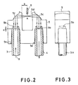
- Fig. 2 and Fig. 3 show the transmission path in the light-conducting prism 5.
- the light-conducting prism 5 has spherical corner-reflecting surfaces 5c.
- the beam 9 emitted from the end of emitting optical fiber 3 at a dispersion angle of about 60 degrees is converged through the focusing lens 5b formed at the entering area on the light-conducting prism 5 so as to compensate the dispersion. Then, the beam 9 is reflected at the central area of the left corner-reflecting surface 5c, and is focused at the point A at the center of the air gap 5d.
- the end faces of the optical fibers are separated from the surface of the prism made of resin, and hence, damage of the prism caused by friction between the prism and optical fibers can be avoided.
- the construction shown in Fig. 1 has no mechanical portion causing friction because the actuator 6 is supported by means of the coil spring 7 in the housing 1. As a result, the movement of the actuator 6 does not produce dust which causes the contamination of the optical components in the optical switch, thus maintaining a good operation.
- the beam 9, emitted from the end of emitting optical fiber 3 corresponding to the focal point F2 is reflected at the corner-reflecting surface 5c, and is focused at the focal point F1 in the air gap 5d.
- the beam 9 is reflected at the right corner-reflecting surface 5c, and is focused onto the focal point F2 which corresponds to the end of receiving optical fiber 4.
- the entire beam 9 emitted from the emitting optical fiber 3 is transmitted to the receiving optical fiber 4 without leakage to the outside.
- the beam 9 is focused at the focal point F1, which corresponds to the center of the air gap 5d in which the shutter 8 moves, a slight movement of the shutter 8 is sufficient to switch the beam 9 on and off.
- Fig. 6 shows a variation of the embodiment shown in Fig. 4.
- the light-conducting prism 5 has two focusing lenses 5b: one is formed opposite the light-emitting end of emitting optical fiber 3; and the other is formed opposite the light-accepting end of receiving optical fiber 4.
- Each focal point of the focusing lenses 5b is designed so as to agree with the second focal point F2 of elliptical corner-reflecting surfaces 5c, as shown in Fig. 6.
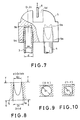
- the optical-fiber-insertion hole 5a provided in the light-conducting prism 5 is a cylindrical hole whose inner diameter D is specified to match the outer diameter d of the optical fibers 3 and 4.
- the outer diameter d of the optical fibers varies somewhat within a tolerance, and hence the inner diameter D of the optical-fiber-insertion hole 5a must be specified to the maximum diameter allowed by the tolerance so that the optical fiber can be inserted into the optical-fiber-insertion holes 5a.
- the diameter D2 above is specified to be greater than the core diameter d0 of the optical fiber, and hence, d > D2 > d0.
- the core diameter d0 is defined as the diameter of the core of the optical fiber which is covered with a sheath made of a flexible resin.
- the sheath at each tip of the optical fibers 3 and 4 is pushed into the optical-fiber-insertion hole 5a and is slightly depressed.
- the optical fibers are connected to the optical-fiber-insertion hole 5a with interference fit.
- Parts of the sheath protruded by the depression are contained in the four innermost corners of the tapered optical-fiber-insertion hole 5a whose cross section is a square.
- the diameter D1 at the entrance of the optical-fiber-insertion hole 5a is greater than the outer diameter d of the optical fiber. This facilitates the inserting operation of the optical fibers into the optical-fiber-insertion holes 5a, making it easier to carry out the connecting operation of the optical fibers to the light-conducting prism 5 under working conditions.
- the optical fibers 3 and 4 fit tightly into the optical-fiber-insertion holes 5a, and that the center line O2 of each end of the optical fibers 3 and 4 are aligned with the optical axis O1 of the focusing lens 5b formed on the light-conducting prism 5.
- the optical fibers 3 and 4 are positioned at the correct locations and are firmly held.
- the optical fibers 3 and 4 can always be positioned correctly as long as the outer diameters d of the optical fibers are within the tolerance. This not only increases the optical transmission rate, but also stabilizes the switching operation of the optical switch.
- Figs. 11 and 12 show a detailed construction of the terminal base 2 for connecting the optical fibers.
- the terminal base 2 has a base 2a, and a holder 2b to be fitted to the base 2a.
- the base 2a has three holes 2c opening upwards and two guide holes 2d for inserting optical fibers.
- the two guide holes 2d are provided through the base 2a so as to guide the optical fibers from the front to the back of the base 2a, with either side of the guide holes 2d opening to the holes 2c.
- the holder 2b has three legs 2e, each of which is fitted into the hole 2c. These legs 2e are unitarily formed with a frame that forms the upper surface and both sides of the base 2a.
- a plurality of rib-like projections 2f are provided in a vertical direction.
- Each rib-like projection 2f has a tip having a wedge-shaped cross section.
- each of the optical fibers 3 and 4 is inserted to one of the guide holes 2d of the base 2a from the front, and each is inserted until the tip of the optical fiber reaches the innermost end of the optical-fiber-insertion hole 5a of the light-conducting prism 5 shown in Fig. 7.
- the holder 2b is fitted to the base 2a from the top thereof: after the legs 2e are inserted into the holes 2c of the base 2a, the holder 2b is pushed into the base 2a.
- the optical fibers already inserted into the guide holes 2d are held between the legs 2e so that the rib-like projection 2f cut into the sheaths (covers made of flexible resins) of the optical fibers 3 and 4 in the perpendicular direction of the optical fibers.
- engaging projections 2g provided at the side ends of the frame of the holder 2b, are engaged to notch 2h of the base 2a so that they are fastened to each other.
- This inclination of the beam 9 may cause a reduction of the transmission efficiency of the beam 9 because a part of the beam 9 emitted from the emitting optical fiber 3 is deflected from the correct transmission path and cannot reach the receiving optical fiber 4.
- the beam 9 is dispersed in the air gap 5d in which the shutter 8 moves, and so the beam will not be focused onto one point. As a result, a slight movement of the shutter 8 will not be sufficient to completely cut off the beam 9 traveling across the air gap 5d. This will adversely affect the stable switching of the beam 9.
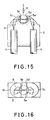
- the inner surfaces of the light-conducting prism 5 which form the boundaries separating the air gap 5d and light-conducting prism 5 have a spherical surface 5e whose center is located at the light-focusing point A at the center of the air gap 5d in which the shutter 8 passes.
- the inclination of the beam 9 from the correct path, which is caused by the refraction of the beam 9, can be eliminated.
- the slightest movement of the shutter 8 is sufficient to switch the beam 9 from the cutoff state to transmitting state, or vice versa, thereby achieving a stable switching of the beam 9.
- FIG. 15 and Fig. 16 A similar effect can be accomplished in the embodiment shown in Fig. 15 and Fig. 16, which has elliptical corner-reflecting surfaces 5c of light-conducting prism 5 for focusing the beam 9 at one point in the air gap 5d.
- the boundaries separating the air gap 5d and the surface areas of the light-conducting prism 5 are also formed spherically as are the surfaces 5e in the embodiment above.
- the light-conducting prism 5 is made by molding a transparent resin.
- a cutting die is required.
- each boundary mentioned above cannot be of a perfect spherical surface: a part of the boundary making contact with the removed section of the cutting die must be of a cylindrical surface. It has, however, been confirmed that this does not adversely affect the function of the optical switch.
- Fig. 17 shows another improved embodiment of the light-conducting prism 5, and this will now be described.
- Pon is the power of the beam 9 transmitted from the emitting optical fiber 3 to the receiving optical fiber 4 when the optical switch is in the ON state
- Poff is the power of the beam 9 transmitted from the emitting optical fiber 3 to the receiving optical fiber 4 when the optical switch is in the OFF state
- the ratio Pon/Poff may be decreased because of stray light produced by reflections of the beam 9 on the shutter 8 and the inner surfaces of the light-conducting prism 5: the beam 9, which is sent into the air gap 5d from the light-conducting prism 5, and is reflected repeatedly producing complicated multi-reflections on the surfaces of the shutter 8 and light-conducting prism 5, can reach the receiving optical fiber 4 passing under the tip of the shutter 8, even if the shutter 8 is plunged into the air gap 5d of the light-conducting prism 5, and hence, the optical switch is in the OFF state.
- the ratio Pon/Poff is decreased, resulting in the degradation of the switching function, particularly the reduction of the dynamic range of the switching.
- the shutter 8 when the shutter 8 is plunged into the air gap 5d of the light-conducting prism 5 as shown in Fig. 17 so as to cut the beam 9 off, the beam 9 reflected on the shutter 8 and deflected from the correct transmission path, will be attenuated by dispersion or absorption on the low-reflectance surfaces 5f before the beam reaches the receiving optical fiber 4.
- Fig. 18 to Fig. 32 show other embodiments of the optical switch having multiple functions: the optical switch described above is partially modified, and a secondary receiving optical fiber is added to the optical switch so that a switch-operation-indicating function or a transfer-switching function can be achieved.
- Fig. 18 shows a basic configuration of the optical switch according to an embodiment, and like numerals refer to like parts in Fig. 1.
- the optical switch in Fig. 18 has a few components heretofore not described in addition to the optical switch shown in Fig. 1: a reflecting body 11 attached to the tip of the shutter 8; and a secondary receiving optical fiber 12 positioned under the reflecting body 11 in such a manner that they are facing each other.
- the actuator 6 is pushed up by means of the coil spring 7, and the reflecting body 11 attached to the shutter 8 is placed in the air gap 5d of the light-conducting prism 5 so as to block the optical path of the beam 9. Accordingly, the beam 9 entering the optical switch through the emitting optical fiber 3 is reflected on the reflecting surface 11a of the reflecting body 11 in the air gap 5d of the light-conducting prism 5, is directed downward and enters the secondary receiving optical fiber 12.
- the beam 9 is not transmitted to the primary receiving optical fiber 4, and hence, the circuit including the primary receiving optical fiber 4 is in the OFF state, whereas the circuit including the secondary receiving optical fiber 12 is in the ON state.
- the beam 9 emitted from the emitting optical fiber 3 passes above the reflecting body 11 in the air gap 5d, travels straight ahead, is reflected on the corner-reflecting surface 5c on the opposite side, and is transmitted to the primary receiving optical fiber 4. Accordingly, in this state, the circuit including the primary receiving optical fiber 4 is in the ON state, whereas the circuit including the secondary receiving optical fiber 12 is in the OFF state.
- Fig. 21 and Fig. 22 show an embodiment which functions in a manner opposite to the embodiment above: the circuit including the primary receiving optical fiber 4 is in the normal ON state, whereas the circuit including the secondary receiving optical fiber 12 is in the normal OFF state.
- the reflecting body 11 of the shutter 8 is located at the top portion of the air gap 5d of the light-conducting prism 5 so that the beam 9 emitted from the emitting optical fiber 3 travels straight forward across the air gap 5d and is transmitted to the receiving optical fiber 4.
- the circuit including the primary receiving optical fiber 4 is in the ON state
- the circuit including the secondary receiving optical fiber 12 is in the OFF state.
- the actuator 6 is pushed down as shown in Fig.
- the beam 9 is reflected on the reflecting surface 11a of the reflecting body 11, and is transmitted to the secondary receiving optical fiber 12.
- the circuit including the primary receiving optical fiber 4 changes to the OFF state
- the circuit including the secondary receiving optical fiber 12 changes to the ON state.
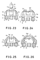
- Fig. 25 shows a light-conducting member having light-conducting prism 5 in which corner-reflecting surfaces 5c are formed in an elliptical surface
- Fig. 26 shows a light-conducting member of a concave reflector 10 as explained in the embodiments in Fig. 4 and Fig. 5.
- the focal points F1 of the elliptical corner-reflecting surfaces 5c and 10c are adjusted to the point A in the air gap 5d in which the reflecting body of shutter 8 (not shown) moves, and the focal points F2 thereof are adjusted to the end faces of the optical fibers 3 and 4.
- the beam 9 emitted from the emitting optical fiber 3 is reflected on the corner-reflecting surface 5c or 10c, and is focused at the point A in the air gap 5d, which corresponds to the focal point F1.
- the beam 9 is collimated by means of the spherical corner-reflecting surface 5c of the light-conducting prism 5, and is sent to the air gap 5d.
- the reflecting surface 11a of the reflecting body 11, which reflects the beam 9 and inclines it towards the secondary receiving optical fiber 12, can be a planar surface.
- the beam 9 is focused at the point A in the air gap 5d of the light-conducting member.
- the beam 9 reflected on the reflecting surface 11a will not be collimated but will be dispersed. This will decrease the transmission efficiency of the beam 9 to the secondary receiving optical fiber 12.
- the reflecting surface 11a of the reflecting body 11 should be made parabolic as shown in Fig. 27 (the light-conducting prism 5 in Fig. 27 has elliptical corner-reflecting surfaces 5c) and in Fig. 28 (the concave reflector 10 in Fig.
- focusing lens 5g or 10g is provided at the incident area of the inclined beam 9 on the light-conducting member so as to face the end face of the secondary receiving optical fiber 12.
- the beam 9 reflected and inclined at the reflecting body 11 is focused onto the end face of the secondary receiving optical fiber 12 through the lens 5g or 10g.
- the light-conducting prism 5 shown in Fig. 23 which collimates the beam 9 to be converged in the air gap 5d, and has a reflecting body 11 with planar reflecting surfaces 11a
- the following problem is presented: the amount of the beam 9 incident to the secondary receiving optical fiber 12 will be greatly changed by a slightest displacement of the reflecting body 11. The reason of this will be described with reference to Fig. 36 to Fig. 38.
- Figs. 37 and 38 show the stroke positions when the reflecting body 11 is positioned lower than the correct position in Fig. 36. In contrast, when the stroke position is located higher than the correct position, a part of the beam 9 passes under the tip of the reflecting body 11, and is transmitted to the primary receiving optical fiber 4, resulting in unstable switching.
- the reflecting surface 11a of the reflecting body 11 is formed in a terraced configuration having steps each of which is composed of a vertical plane and an oblique plane meeting at 45 degrees with the vertical plane. Comparing the reflecting body 11 in Fig. 29 with that in Fig. 36, it is seen that the reflecting surface area M of the reflecting body 11 in Fig. 29 is greater than the reflecting surface area m in Fig. 36 (M > m) when the widths of the reflecting bodies 11 in Figs. 29 and 36 are the same. Accordingly, a slight displacement of the stroke position of the reflecting body 11 as shown in Fig. 30 to Fig.
Landscapes
- Physics & Mathematics (AREA)
- General Physics & Mathematics (AREA)
- Optics & Photonics (AREA)
- Mechanical Light Control Or Optical Switches (AREA)
- Switches Operated By Changes In Physical Conditions (AREA)
- Push-Button Switches (AREA)
- Electronic Switches (AREA)
- Optical Couplings Of Light Guides (AREA)
Priority Applications (1)
| Application Number | Priority Date | Filing Date | Title |
|---|---|---|---|
| EP96103679A EP0718657B1 (de) | 1988-12-29 | 1989-12-27 | Optischer Schalter |
Applications Claiming Priority (10)
| Application Number | Priority Date | Filing Date | Title |
|---|---|---|---|
| JP332811/88 | 1988-12-29 | ||
| JP33281188 | 1988-12-29 | ||
| JP149806/89 | 1989-06-13 | ||
| JP14980689 | 1989-06-13 | ||
| JP226818/89 | 1989-09-01 | ||
| JP22681889 | 1989-09-01 | ||
| JP250304/89 | 1989-09-26 | ||
| JP25030489 | 1989-09-26 | ||
| JP314654/89 | 1989-12-04 | ||
| JP1314654A JPH088027B2 (ja) | 1988-12-29 | 1989-12-04 | 光スイッチ |
Related Child Applications (2)
| Application Number | Title | Priority Date | Filing Date |
|---|---|---|---|
| EP96103679A Division EP0718657B1 (de) | 1988-12-29 | 1989-12-27 | Optischer Schalter |
| EP96103679.5 Division-Into | 1989-12-27 |
Publications (3)
| Publication Number | Publication Date |
|---|---|
| EP0379732A2 true EP0379732A2 (de) | 1990-08-01 |
| EP0379732A3 EP0379732A3 (de) | 1991-05-08 |
| EP0379732B1 EP0379732B1 (de) | 1996-09-18 |
Family
ID=27527886
Family Applications (2)
| Application Number | Title | Priority Date | Filing Date |
|---|---|---|---|
| EP89124008A Expired - Lifetime EP0379732B1 (de) | 1988-12-29 | 1989-12-27 | Optischer Schalter |
| EP96103679A Expired - Lifetime EP0718657B1 (de) | 1988-12-29 | 1989-12-27 | Optischer Schalter |
Family Applications After (1)
| Application Number | Title | Priority Date | Filing Date |
|---|---|---|---|
| EP96103679A Expired - Lifetime EP0718657B1 (de) | 1988-12-29 | 1989-12-27 | Optischer Schalter |
Country Status (3)
| Country | Link |
|---|---|
| EP (2) | EP0379732B1 (de) |
| JP (1) | JPH088027B2 (de) |
| DE (2) | DE68927227T2 (de) |
Cited By (9)
| Publication number | Priority date | Publication date | Assignee | Title |
|---|---|---|---|---|
| WO1992020154A1 (de) * | 1991-04-26 | 1992-11-12 | Daimler-Benz Aktiengesellschaft | Gabellichtschranke |
| EP0550017A3 (en) * | 1991-12-31 | 1994-08-10 | Texas Instruments Inc | Fiber optic switch with spatial light modulator device |
| DE4332748A1 (de) * | 1993-09-25 | 1995-03-30 | Marquardt Gmbh | Schalter, vorzugsweise für Kraftfahrzeug |
| DE4336729A1 (de) * | 1993-10-28 | 1995-05-04 | Marquardt Gmbh | Optischer Schalter |
| WO1998015094A1 (en) * | 1996-09-30 | 1998-04-09 | Ericsson Inc. | Foldable cellular telephone with flip on/off detector |
| DE19748131A1 (de) * | 1997-10-31 | 1999-06-24 | Kostal Leopold Gmbh & Co Kg | Vorrichtung zum Erfassen von Schaltstellungen eines mechanisch betätigbaren Schaltmittels sowie Verfahren zum Erfassen von Schaltstellungen eines mechanisch betätigbaren Schaltmittels |
| WO2001038922A3 (en) * | 1999-11-23 | 2002-09-12 | Nanovation Tech Inc | Analog optical switch using an integrated mach-zehnder interferometer having a movable phase shifter |
| CN102426947A (zh) * | 2011-08-31 | 2012-04-25 | 瑞电士(常熟)传感器有限公司 | 红外线光电开关壳体 |
| CN111735481A (zh) * | 2020-07-15 | 2020-10-02 | 合肥知常光电科技有限公司 | 一种多路光开关同步快速切换控制系统及其控制方法 |
Families Citing this family (14)
| Publication number | Priority date | Publication date | Assignee | Title |
|---|---|---|---|---|
| US6580849B2 (en) * | 2001-01-05 | 2003-06-17 | Agilent Technologies, Inc. | Optical switch incorporating stepped faceted mirrors |
| GB0201969D0 (en) | 2002-01-29 | 2002-03-13 | Qinetiq Ltd | Integrated optics devices |
| ATE344468T1 (de) * | 2002-02-15 | 2006-11-15 | Omron Tateisi Electronics Co | Optisches kopplungselement und transceiver, der es benutzt |
| JP2003307603A (ja) | 2002-02-15 | 2003-10-31 | Omron Corp | 光学素子及び当該素子を用いた光学部品 |
| GB0208048D0 (en) * | 2002-04-08 | 2002-05-22 | Digicliff Ltd | Optical controls |
| GB0306008D0 (en) | 2003-03-15 | 2003-04-23 | Qinetiq Ltd | Optical device |
| GB0306638D0 (en) | 2003-03-22 | 2003-04-30 | Qinetiq Ltd | Optical routing device |
| GB0306634D0 (en) | 2003-03-22 | 2003-04-30 | Qinetiq Ltd | Optical wavelength division multiplexer/demultiplexer device |
| JP3985269B2 (ja) * | 2004-09-29 | 2007-10-03 | 松下電工株式会社 | 光スイッチ |
| FR2878339B1 (fr) * | 2004-11-22 | 2007-02-09 | Commissariat Energie Atomique | Dispositif d'egalisation de chemins optiques suivis par une pluralite de faisceaux optiques |
| JP2008119249A (ja) * | 2006-11-13 | 2008-05-29 | Ge Medical Systems Global Technology Co Llc | 操作スイッチ装置および磁気共鳴イメージング装置 |
| DE102012206417A1 (de) * | 2012-04-19 | 2013-10-24 | Zf Friedrichshafen Ag | Schalthebelvorrichtung zur Betätigung eines Fahrzeuggetriebes |
| CN113066684B (zh) * | 2021-03-30 | 2023-01-17 | 新疆心连心能源化工有限公司 | 远程光控按钮、远程光控箱及远程控制装置 |
| EP4490559A4 (de) * | 2022-03-09 | 2026-03-04 | Banner Eng | Optoelektronische notstoppvorrichtung |
Family Cites Families (10)
| Publication number | Priority date | Publication date | Assignee | Title |
|---|---|---|---|---|
| US4315147A (en) * | 1980-02-15 | 1982-02-09 | Battelle Memorial Institute | Photoelectric switch with visible signal |
| JPS6235237Y2 (de) * | 1980-09-20 | 1987-09-08 | ||
| JPS5889727A (ja) * | 1981-11-24 | 1983-05-28 | オムロン株式会社 | 無接点マイクロスイツチ |
| FR2527793A1 (fr) * | 1982-05-27 | 1983-12-02 | Souriau & Cie | Commutateur optique |
| US4607160A (en) * | 1982-09-21 | 1986-08-19 | Omron Tateisi Electronics Co. | Non-contact switching device |
| JPS6012217U (ja) * | 1983-07-01 | 1985-01-28 | オムロン株式会社 | 光マイクロスイツチ |
| JPS6042222U (ja) * | 1983-08-31 | 1985-03-25 | オムロン株式会社 | 光マイクロスイッチ |
| JPS6042223U (ja) * | 1983-08-31 | 1985-03-25 | オムロン株式会社 | 光マイクロスイッチ |
| JPS61721U (ja) * | 1984-06-08 | 1986-01-07 | 株式会社山武 | 光開閉装置 |
| JPS6235237U (de) * | 1985-08-22 | 1987-03-02 |
-
1989
- 1989-12-04 JP JP1314654A patent/JPH088027B2/ja not_active Expired - Lifetime
- 1989-12-27 EP EP89124008A patent/EP0379732B1/de not_active Expired - Lifetime
- 1989-12-27 EP EP96103679A patent/EP0718657B1/de not_active Expired - Lifetime
- 1989-12-27 DE DE68927227T patent/DE68927227T2/de not_active Expired - Fee Related
- 1989-12-27 DE DE68929386T patent/DE68929386T2/de not_active Expired - Fee Related
Cited By (13)
| Publication number | Priority date | Publication date | Assignee | Title |
|---|---|---|---|---|
| WO1992020154A1 (de) * | 1991-04-26 | 1992-11-12 | Daimler-Benz Aktiengesellschaft | Gabellichtschranke |
| EP0550017A3 (en) * | 1991-12-31 | 1994-08-10 | Texas Instruments Inc | Fiber optic switch with spatial light modulator device |
| DE4332748A1 (de) * | 1993-09-25 | 1995-03-30 | Marquardt Gmbh | Schalter, vorzugsweise für Kraftfahrzeug |
| DE4332748B4 (de) * | 1993-09-25 | 2009-01-15 | Marquardt Gmbh | Schalter, vorzugsweise für Kraftfahrzeug |
| DE4336729C2 (de) * | 1993-10-28 | 2003-04-24 | Marquardt Gmbh | Optischer Schalter |
| DE4336729A1 (de) * | 1993-10-28 | 1995-05-04 | Marquardt Gmbh | Optischer Schalter |
| US5918188A (en) * | 1996-09-30 | 1999-06-29 | Ericsson Inc. | Flip on/off detector |
| WO1998015094A1 (en) * | 1996-09-30 | 1998-04-09 | Ericsson Inc. | Foldable cellular telephone with flip on/off detector |
| DE19748131A1 (de) * | 1997-10-31 | 1999-06-24 | Kostal Leopold Gmbh & Co Kg | Vorrichtung zum Erfassen von Schaltstellungen eines mechanisch betätigbaren Schaltmittels sowie Verfahren zum Erfassen von Schaltstellungen eines mechanisch betätigbaren Schaltmittels |
| DE19748131C2 (de) * | 1997-10-31 | 1999-10-14 | Kostal Leopold Gmbh & Co Kg | Vorrichtung zum Erfassen von Schaltstellungen eines mechanisch betätigbaren Schaltmittels sowie Verfahren zum Erfassen von Schaltstellungen eines mechanisch betätigbaren Schaltmittels |
| WO2001038922A3 (en) * | 1999-11-23 | 2002-09-12 | Nanovation Tech Inc | Analog optical switch using an integrated mach-zehnder interferometer having a movable phase shifter |
| CN102426947A (zh) * | 2011-08-31 | 2012-04-25 | 瑞电士(常熟)传感器有限公司 | 红外线光电开关壳体 |
| CN111735481A (zh) * | 2020-07-15 | 2020-10-02 | 合肥知常光电科技有限公司 | 一种多路光开关同步快速切换控制系统及其控制方法 |
Also Published As
| Publication number | Publication date |
|---|---|
| EP0718657A3 (de) | 1996-09-04 |
| EP0718657B1 (de) | 2002-04-03 |
| DE68929386T2 (de) | 2002-11-21 |
| EP0379732A3 (de) | 1991-05-08 |
| DE68927227D1 (de) | 1996-10-24 |
| DE68929386D1 (de) | 2002-05-08 |
| JPH088027B2 (ja) | 1996-01-29 |
| JPH03190019A (ja) | 1991-08-20 |
| EP0379732B1 (de) | 1996-09-18 |
| DE68927227T2 (de) | 1997-04-24 |
| EP0718657A2 (de) | 1996-06-26 |
Similar Documents
| Publication | Publication Date | Title |
|---|---|---|
| US5175780A (en) | Optical fiber switch | |
| EP0718657B1 (de) | Optischer Schalter | |
| JP2855744B2 (ja) | 反射形光電スイッチ | |
| US5028110A (en) | Fiber optical component | |
| US4812003A (en) | Optic sensing assembly | |
| US7254296B2 (en) | Apparatus for improved fiber optic coupling efficiency | |
| US6832031B2 (en) | Optical modifier and method for the manufacture thereof | |
| US5361315A (en) | Refractive element optical transmission switch | |
| US4346292A (en) | Coaxial optical scanner | |
| US6870988B2 (en) | Tap outlet collimator | |
| US6910810B2 (en) | Optical part for two-way optical communication | |
| US7212721B2 (en) | Variable optical attenuator | |
| CN108490556B (zh) | 光模块 | |
| JP2550509B2 (ja) | 光スイッチ | |
| US6707960B2 (en) | Reflection type compact optical switch | |
| KR20000067535A (ko) | 광소자모듈 | |
| US4439029A (en) | Camera with information transmitting elements | |
| US12613384B2 (en) | Optical transceiver having tilted optical fibers | |
| KR100771765B1 (ko) | 광 스위치 | |
| JP3890128B2 (ja) | 反射型プリズム | |
| EP0289185B1 (de) | Optische Sensoranordnung | |
| US7324575B2 (en) | Lens with reflective surface | |
| CN114303251B (zh) | 半导体受光模块 | |
| CN108873192B (zh) | 光模块 | |
| KR200271879Y1 (ko) | 이중기능을 가진 초점 구조체 |
Legal Events
| Date | Code | Title | Description |
|---|---|---|---|
| PUAI | Public reference made under article 153(3) epc to a published international application that has entered the european phase |
Free format text: ORIGINAL CODE: 0009012 |
|
| 17P | Request for examination filed |
Effective date: 19900129 |
|
| AK | Designated contracting states |
Kind code of ref document: A2 Designated state(s): CH DE GB LI |
|
| PUAL | Search report despatched |
Free format text: ORIGINAL CODE: 0009013 |
|
| AK | Designated contracting states |
Kind code of ref document: A3 Designated state(s): CH DE GB LI |
|
| 17Q | First examination report despatched |
Effective date: 19930507 |
|
| GRAH | Despatch of communication of intention to grant a patent |
Free format text: ORIGINAL CODE: EPIDOS IGRA |
|
| GRAH | Despatch of communication of intention to grant a patent |
Free format text: ORIGINAL CODE: EPIDOS IGRA |
|
| GRAA | (expected) grant |
Free format text: ORIGINAL CODE: 0009210 |
|
| AK | Designated contracting states |
Kind code of ref document: B1 Designated state(s): CH DE GB LI |
|
| XX | Miscellaneous (additional remarks) |
Free format text: TEILANMELDUNG 96103679.5 EINGEREICHT AM 08/03/96. |
|
| REF | Corresponds to: |
Ref document number: 68927227 Country of ref document: DE Date of ref document: 19961024 |
|
| REG | Reference to a national code |
Ref country code: CH Ref legal event code: NV Representative=s name: BOVARD AG PATENTANWAELTE |
|
| PLBE | No opposition filed within time limit |
Free format text: ORIGINAL CODE: 0009261 |
|
| STAA | Information on the status of an ep patent application or granted ep patent |
Free format text: STATUS: NO OPPOSITION FILED WITHIN TIME LIMIT |
|
| 26N | No opposition filed | ||
| PGFP | Annual fee paid to national office [announced via postgrant information from national office to epo] |
Ref country code: GB Payment date: 19981231 Year of fee payment: 10 |
|
| PGFP | Annual fee paid to national office [announced via postgrant information from national office to epo] |
Ref country code: DE Payment date: 19990107 Year of fee payment: 10 |
|
| PGFP | Annual fee paid to national office [announced via postgrant information from national office to epo] |
Ref country code: CH Payment date: 19990115 Year of fee payment: 10 |
|
| PG25 | Lapsed in a contracting state [announced via postgrant information from national office to epo] |
Ref country code: GB Free format text: LAPSE BECAUSE OF NON-PAYMENT OF DUE FEES Effective date: 19991227 |
|
| PG25 | Lapsed in a contracting state [announced via postgrant information from national office to epo] |
Ref country code: LI Free format text: LAPSE BECAUSE OF NON-PAYMENT OF DUE FEES Effective date: 19991231 Ref country code: CH Free format text: LAPSE BECAUSE OF NON-PAYMENT OF DUE FEES Effective date: 19991231 |
|
| GBPC | Gb: european patent ceased through non-payment of renewal fee |
Effective date: 19991227 |
|
| PG25 | Lapsed in a contracting state [announced via postgrant information from national office to epo] |
Ref country code: DE Free format text: LAPSE BECAUSE OF NON-PAYMENT OF DUE FEES Effective date: 20001003 |