EP0379955A1 - Circuit ECL et son utilisation en connexion avec un oscillateur contrôlé par voltage - Google Patents
Circuit ECL et son utilisation en connexion avec un oscillateur contrôlé par voltage Download PDFInfo
- Publication number
- EP0379955A1 EP0379955A1 EP90100908A EP90100908A EP0379955A1 EP 0379955 A1 EP0379955 A1 EP 0379955A1 EP 90100908 A EP90100908 A EP 90100908A EP 90100908 A EP90100908 A EP 90100908A EP 0379955 A1 EP0379955 A1 EP 0379955A1
- Authority
- EP
- European Patent Office
- Prior art keywords
- transistor
- collector
- input
- current source
- supply voltage
- Prior art date
- Legal status (The legal status is an assumption and is not a legal conclusion. Google has not performed a legal analysis and makes no representation as to the accuracy of the status listed.)
- Withdrawn
Links
- 238000012358 sourcing Methods 0.000 claims description 4
- 230000003750 conditioning effect Effects 0.000 claims 1
- 238000010586 diagram Methods 0.000 description 7
- 238000005516 engineering process Methods 0.000 description 4
- 230000007850 degeneration Effects 0.000 description 2
- 238000009738 saturating Methods 0.000 description 2
- 239000003990 capacitor Substances 0.000 description 1
- 150000001875 compounds Chemical class 0.000 description 1
- 230000001934 delay Effects 0.000 description 1
- 238000000034 method Methods 0.000 description 1
- 230000003278 mimic effect Effects 0.000 description 1
- 230000000737 periodic effect Effects 0.000 description 1
- 230000007704 transition Effects 0.000 description 1
Images

Classifications
-
- H—ELECTRICITY
- H03—ELECTRONIC CIRCUITRY
- H03K—PULSE TECHNIQUE
- H03K3/00—Circuits for generating electric pulses; Monostable, bistable or multistable circuits
- H03K3/02—Generators characterised by the type of circuit or by the means used for producing pulses
- H03K3/027—Generators characterised by the type of circuit or by the means used for producing pulses by the use of logic circuits, with internal or external positive feedback
- H03K3/03—Astable circuits
- H03K3/0315—Ring oscillators
-
- H—ELECTRICITY
- H03—ELECTRONIC CIRCUITRY
- H03K—PULSE TECHNIQUE
- H03K5/00—Manipulating of pulses not covered by one of the other main groups of this subclass
- H03K5/13—Arrangements having a single output and transforming input signals into pulses delivered at desired time intervals
- H03K5/133—Arrangements having a single output and transforming input signals into pulses delivered at desired time intervals using a chain of active delay devices
-
- H—ELECTRICITY
- H03—ELECTRONIC CIRCUITRY
- H03L—AUTOMATIC CONTROL, STARTING, SYNCHRONISATION OR STABILISATION OF GENERATORS OF ELECTRONIC OSCILLATIONS OR PULSES
- H03L7/00—Automatic control of frequency or phase; Synchronisation
- H03L7/06—Automatic control of frequency or phase; Synchronisation using a reference signal applied to a frequency- or phase-locked loop
- H03L7/08—Details of the phase-locked loop
- H03L7/099—Details of the phase-locked loop concerning mainly the controlled oscillator of the loop
- H03L7/0995—Details of the phase-locked loop concerning mainly the controlled oscillator of the loop the oscillator comprising a ring oscillator
-
- H—ELECTRICITY
- H03—ELECTRONIC CIRCUITRY
- H03K—PULSE TECHNIQUE
- H03K5/00—Manipulating of pulses not covered by one of the other main groups of this subclass
- H03K2005/00013—Delay, i.e. output pulse is delayed after input pulse and pulse length of output pulse is dependent on pulse length of input pulse
- H03K2005/0015—Layout of the delay element
- H03K2005/00195—Layout of the delay element using FET's
- H03K2005/00208—Layout of the delay element using FET's using differential stages
Definitions
- the present invention relates to clock generators and, in particular, to an emitter-coupled logic (ECL) gate configuration that allows variations in the bias current for controlling propagation delay.
- ECL emitter-coupled logic
- the disclosed ECL gate configuration has particular application in a voltage controlled ring oscillator.
- a voltage controlled oscillator (VCO) generates periodic signals which are converted into a square wave output which can be used to provide timing pulses in various logic circuits.
- the output frequency of a VCO is a function of its input control voltage.
- VCOs are commonly used in phase-locked loop (PLL) circuits.
- a general purpose PLL 10 typically includes a phase comparator 12, a low-pass filter 14 with some gain, and a VCO 16.
- the phase comparator 12 compares the frequency and the phase of the input signal and of the VCO 16 and generates either a positive or a negative error voltage V e which is filtered and applied, as V d , to the VCO 16. If the input signal is within the capture range of the PLL 10, then the VCO 16 will lock onto the input frequency f s and generate an output signal of the same frequency as f s with a small fixed phase difference. Once the VCO 16 is locked onto the input signal, its output frequency f o will vary over the locking range as the input frequency f s varies.
- TTL logic gate circuitry utilized for this purpose is shown in Fig. 2. It includes three series-connected, TTL gates comprising Schottky-clamped NPN transistors T1, T2 and T3, respectively, together with corresponding load resistors R1, R2 and R3. As shown in Fig. 2, the output of this TTL gate configuration can be controlled by adjusting the supply voltage V CC applied to the load resistors R1, R2 and R3.
- TTL technology represents a compromise between speed and power.
- the speed-power product of this technology is approximately linear. That is, increased speed results in increased power dissipation, and vice versa, up to a point at which the maximum speed limitation of the gate is reached.
- TTL circuits use transistors in the saturating mode. Therefore, as stated above, while they experience relatively low power dissipation, TTL circuits do not possess the speed characteristics required in some applications.
- Emitter-coupled logic (ECL) technology does not allow transistors to saturate. Therefore, ECL gate speeds can be maximized.
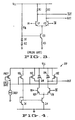
- Fig. 3 shows a conventional, non-saturating ECL gate configuration. It includes two differential NPN input transistors E1 and E2 with corresponding load resistors R1 and R2 connected between the collectors of the respective devices E1 and E2 and the supply voltage V CC . Two diodes D1 and D2, together with resistor R B , bias the base of NPN current source transistor E3 to a two diode level, thus providing a one diode voltage drop across current source resistor R3. This ensures that the voltage swing of resistors R1 and R2 is also one diode since the emitter current and collector current of devices E1 and E2 will be equal, input devices E1 and E2 being configured as an emitter-coupled pair.
- the logic swing of the ECL gate shown in Fig. 3 is controlled by the fact that the two load resistors R1 and R2 and the current source resistor R3 are matched.
- the propagation delay of the gate is determined by the power level set by the load resistors R1 and R2.
- the ECL gate shown in Fig. 3 is basically a differential amplifier with load resistors R1 and R2 that are kept small enough in value to allow corresponding input transistors E1 and E2 to remain out of saturation, even when the differential amplifier is fully switched so that only one of the input transistors E1 or E2 is "on.”
- Claims 1, 3, 6, and 9 define respectively such circuitry in accordance with the present invention.
- Claims 10 and 12 define VDCO's in connection with such circuits.
- the present invention provides an emitter-coupled logic (ECL) gate configuration that allows variations in the bias current for controlling propagation delay.
- the ECL circuitry includes a plurality of input transistors having commonly-coupled emitters in the conventional manner, the collector of each input transistor being connected to receive a control voltage.
- a current source is connected between the commonly-coupled emitters and ground.
- Circuitry preferably a variable resistance, is connected between the collectors of the input transistors and a supply voltage.
- a bias voltage controls the charging current provided to the collectors of the ECL input transistors.
- the emitter-coupled logic gate includes first and second NPN input transistors having commonly-coupled emitters.
- the base of the first input transistor is connected to receive a first input signal.
- the base of the second input transistor is connected to receive a second input signal.
- a first PMOS transistor and a first Schottky diode are connected in parallel between a supply voltage VCC and the collector of the first input transistor.
- a second PMOS transistor and a second Schottky diode are connected in parallel between VCC and the collector of the second input transistor.
- a first NPN current source transistor has its emitter coupled to ground.
- a third PMOS transistor is connected between the common base/collector terminal of the first current source transistor and VCC.
- a second NPN current source transistor is connected between the commonly-coupled emitters of the first and second input transistors and ground.
- the base of the second current source transistor is connected to the common base/collector terminal of the first current source transistor.
- the second current source transistor has twice the current sourcing capability of the first current source transistor.
- a gate bias voltage is applied to the gate of each of the three PMOS transistors to control the propagation delay of the gate.
- the present invention provides an ECL gate configuration 100 that allows the bias current applied to the gate 100 to be varied. This permits the propagation delay of the gate 100 to be changed by way of an input control voltage. Controlling the propagation delay in this manner allows the ECL gate 100 to be used in voltage controlled oscillator applications, as will be described in greater detail below.
- the structure of the ECL gate 100 is similar to a standard ECL logic gate except that each of the conventional ECL gate collector load resistors is replaced by a PMOS device 102 in parallel with a Schottky diode 104.
- This configuration makes it possible to vary the gate's effective logic switching currents and propagation delays because the gate bias of the PMOS devices 102 can be varied to mimic an adjustable load resistor.
- a Schottky diode 102 is present to limit the low level logic swing.
- the pull-down current source comprising NPN devices 1X and 2X, for the gate 100 is controlled by an identically biased PMOS control transistor 106.
- Device 2X has twice the current sourcing capability of device 1X.
- the current of device 106 is scaled up to be twice that of the upper PMOS source, i.e. elements 102 and 104, so that, during transitions, the charging currents at the collectors of the input transistors 108, 110 are matched.
- the collector of the common-emitter, differential pair NPN transistor, i.e. either device 108 or device 110, which is “off” is held at a logic “high” level by one of the PMOS devices 102 at a 1X current sourcing magnitude.
- the collector of the differential pair NPN transistor (108, 110) which is “on” is held “low” at one Schottky diode voltage drop below VCC by the pulldown current source device 2X.
- the 2X current for the "low” level collector comprises 1X sourced by the appropriate PMOS device 102 and 1X sourced by the corresponding Schottky diode 104.
- the net positive charging current is 1X.
- the net negative charging current is also 1X as a result of the 1X DC currents demanded of the PMOS device 102, which is always "on" independent of its logic state.
- ECL gate 100 is a current-to-voltage converter, comprising current source IREF and PMOS device PREF, which provides a linear current and, thus, eliminates the non-linear V gs voltage attributes of PMOS devices 102 and 106.
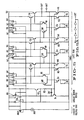
- Fig. 5 shows a three-stage voltage controlled ring oscillator that utilizes three ECL gates 100 of the type described above. Like numerals in Figs. 4 and 5 identify corresponding circuit elements.
- the simple current mirror shown in Fig. 4 as including current source devices 1X and 2X has been modified to provide a more conventional compound current mirror structure.
- NPN devices 112 and 114 have been added as current sources for the emitter followers 120.
- Degeneration resistors 116 have been added.
- two half-value emitter degeneration resistors 118 have been added between ground and each of devices 2X.
Landscapes
- Physics & Mathematics (AREA)
- Nonlinear Science (AREA)
- Logic Circuits (AREA)
- Stabilization Of Oscillater, Synchronisation, Frequency Synthesizers (AREA)
Applications Claiming Priority (2)
| Application Number | Priority Date | Filing Date | Title |
|---|---|---|---|
| US07/299,768 US4876519A (en) | 1989-01-23 | 1989-01-23 | High frequency ECL voltage controlled ring oscillator |
| US299768 | 1989-01-23 |
Publications (1)
| Publication Number | Publication Date |
|---|---|
| EP0379955A1 true EP0379955A1 (fr) | 1990-08-01 |
Family
ID=23156216
Family Applications (1)
| Application Number | Title | Priority Date | Filing Date |
|---|---|---|---|
| EP90100908A Withdrawn EP0379955A1 (fr) | 1989-01-23 | 1990-01-17 | Circuit ECL et son utilisation en connexion avec un oscillateur contrôlé par voltage |
Country Status (4)
| Country | Link |
|---|---|
| US (1) | US4876519A (fr) |
| EP (1) | EP0379955A1 (fr) |
| JP (1) | JPH02233012A (fr) |
| CA (1) | CA1303690C (fr) |
Cited By (1)
| Publication number | Priority date | Publication date | Assignee | Title |
|---|---|---|---|---|
| EP0820146A3 (fr) * | 1996-07-16 | 1999-07-28 | Seiko Epson Corporation | Elément différentiel à retard servant à éviter l'oscillation en mode commun et l'hysterésis d'entrée |
Families Citing this family (23)
| Publication number | Priority date | Publication date | Assignee | Title |
|---|---|---|---|---|
| US5061907A (en) * | 1991-01-17 | 1991-10-29 | National Semiconductor Corporation | High frequency CMOS VCO with gain constant and duty cycle compensation |
| US5283479A (en) * | 1991-04-30 | 1994-02-01 | Microunity Systems Engineering, Inc. | BiCMOS logic gate having plural linearly operated load FETs |
| US5231314A (en) * | 1992-03-02 | 1993-07-27 | National Semiconductor Corporation | Programmable timing circuit for integrated circuit device with test access port |
| US5179358A (en) * | 1992-03-04 | 1993-01-12 | Motorola, Inc. | Circuit, counter and frequency synthesizer with adjustable bias current |
| US5191301A (en) * | 1992-05-12 | 1993-03-02 | International Business Machines Corporation | Integrated differential voltage controlled ring oscillator |
| US5206609A (en) * | 1992-05-15 | 1993-04-27 | Motorola, Inc. | Current controlled oscillator with linear output frequency |
| US5239274A (en) * | 1992-05-26 | 1993-08-24 | Digital Equipment Corporation | Voltage-controlled ring oscillator using complementary differential buffers for generating multiple phase signals |
| US5285173A (en) * | 1992-07-13 | 1994-02-08 | Analog Devices, Inc. | Signal-controlled ring oscillator with delay cells having constant gain with change in frequency |
| US5317287A (en) | 1992-07-16 | 1994-05-31 | National Semiconductor Corporation | Low-gain, range programmable, temperature compensated voltage controlled ring oscillator |
| US5300898A (en) * | 1992-07-29 | 1994-04-05 | Ncr Corporation | High speed current/voltage controlled ring oscillator circuit |
| US5389833A (en) * | 1992-08-27 | 1995-02-14 | Texas Instruments Incorporated | Analog multiplexer |
| DE69411217T2 (de) * | 1993-04-05 | 1999-02-04 | Philips Electronics N.V., Eindhoven | Verzögerungsschaltung zum Verzögern von differentiellen Signalen |
| EP0619650B1 (fr) * | 1993-04-05 | 1998-06-24 | Koninklijke Philips Electronics N.V. | Circuit de rétard pour retarder des signaux différentiels |
| US5428626A (en) * | 1993-10-18 | 1995-06-27 | Tektronix, Inc. | Timing analyzer for embedded testing |
| US5619161A (en) * | 1994-08-31 | 1997-04-08 | International Business Machines Corporation | Diffrential charge pump with integrated common mode control |
| US5495207A (en) * | 1994-08-31 | 1996-02-27 | International Business Machines Corporation | Differential current controlled oscillator with variable load |
| US5491439A (en) * | 1994-08-31 | 1996-02-13 | International Business Machines Corporation | Method and apparatus for reducing jitter in a phase locked loop circuit |
| US5513225A (en) * | 1994-08-31 | 1996-04-30 | International Business Machines Corporation | Resistorless phase locked loop circuit employing direct current injection |
| US5525932A (en) * | 1994-08-31 | 1996-06-11 | International Business Machines Corporation | Lock indicator for phase locked loop circuit |
| JP2923910B2 (ja) * | 1996-08-14 | 1999-07-26 | 日本電気株式会社 | 超低利得電圧制御発振器 |
| JP3697847B2 (ja) * | 1997-08-21 | 2005-09-21 | ソニー株式会社 | 電圧制御発振回路 |
| JP2002057558A (ja) * | 2000-08-09 | 2002-02-22 | Fujitsu Ltd | 遅延回路 |
| JP2008054134A (ja) * | 2006-08-25 | 2008-03-06 | Matsushita Electric Ind Co Ltd | リング発振器及びそれを備えた半導体集積回路及び電子機器 |
Citations (8)
| Publication number | Priority date | Publication date | Assignee | Title |
|---|---|---|---|---|
| DE2518861B2 (de) * | 1974-05-02 | 1980-12-04 | Motorola Inc., Schaumburg, Ill. (V.St.A.) | Nichtsättigende Logikschaltung |
| DE3135952A1 (de) * | 1981-09-10 | 1983-04-21 | Siemens AG, 1000 Berlin und 8000 München | Gegentakt-ausgangsschaltung fuer ein verknuepfungsglied in stromschaltertechnik. |
| DE3528550A1 (de) * | 1984-08-09 | 1986-02-20 | Nec Corp., Tokio/Tokyo | Logischer stromumschaltkreis |
| EP0186260A2 (fr) * | 1984-06-29 | 1986-07-02 | Advanced Micro Devices, Inc. | Circuit de porte logique à émetteurs couplés |
| US4695749A (en) * | 1986-02-25 | 1987-09-22 | Fairchild Semiconductor Corporation | Emitter-coupled logic multiplexer |
| GB2201311A (en) * | 1987-01-23 | 1988-08-24 | Grass Valley Group | Low power differential ecl line driver |
| EP0294163A2 (fr) * | 1987-06-02 | 1988-12-07 | Fujitsu Limited | Circuit intégré à semi-conducteurs comportant un circuit émetteur-suiveur |
| US4792706A (en) * | 1986-12-16 | 1988-12-20 | Texas Instruments Incorporated | ECL gates using diode-clamped loads and Schottky clamped reference bias |
Family Cites Families (1)
| Publication number | Priority date | Publication date | Assignee | Title |
|---|---|---|---|---|
| US4565976A (en) * | 1983-08-05 | 1986-01-21 | Advanced Micro Devices, Inc. | Interruptable voltage-controlled oscillator and phase-locked loop using same |
-
1989
- 1989-01-23 US US07/299,768 patent/US4876519A/en not_active Expired - Lifetime
- 1989-09-29 CA CA000614696A patent/CA1303690C/fr not_active Expired - Fee Related
-
1990
- 1990-01-17 EP EP90100908A patent/EP0379955A1/fr not_active Withdrawn
- 1990-01-23 JP JP2011970A patent/JPH02233012A/ja active Pending
Patent Citations (8)
| Publication number | Priority date | Publication date | Assignee | Title |
|---|---|---|---|---|
| DE2518861B2 (de) * | 1974-05-02 | 1980-12-04 | Motorola Inc., Schaumburg, Ill. (V.St.A.) | Nichtsättigende Logikschaltung |
| DE3135952A1 (de) * | 1981-09-10 | 1983-04-21 | Siemens AG, 1000 Berlin und 8000 München | Gegentakt-ausgangsschaltung fuer ein verknuepfungsglied in stromschaltertechnik. |
| EP0186260A2 (fr) * | 1984-06-29 | 1986-07-02 | Advanced Micro Devices, Inc. | Circuit de porte logique à émetteurs couplés |
| DE3528550A1 (de) * | 1984-08-09 | 1986-02-20 | Nec Corp., Tokio/Tokyo | Logischer stromumschaltkreis |
| US4695749A (en) * | 1986-02-25 | 1987-09-22 | Fairchild Semiconductor Corporation | Emitter-coupled logic multiplexer |
| US4792706A (en) * | 1986-12-16 | 1988-12-20 | Texas Instruments Incorporated | ECL gates using diode-clamped loads and Schottky clamped reference bias |
| GB2201311A (en) * | 1987-01-23 | 1988-08-24 | Grass Valley Group | Low power differential ecl line driver |
| EP0294163A2 (fr) * | 1987-06-02 | 1988-12-07 | Fujitsu Limited | Circuit intégré à semi-conducteurs comportant un circuit émetteur-suiveur |
Cited By (1)
| Publication number | Priority date | Publication date | Assignee | Title |
|---|---|---|---|---|
| EP0820146A3 (fr) * | 1996-07-16 | 1999-07-28 | Seiko Epson Corporation | Elément différentiel à retard servant à éviter l'oscillation en mode commun et l'hysterésis d'entrée |
Also Published As
| Publication number | Publication date |
|---|---|
| CA1303690C (fr) | 1992-06-16 |
| US4876519A (en) | 1989-10-24 |
| JPH02233012A (ja) | 1990-09-14 |
Similar Documents
| Publication | Publication Date | Title |
|---|---|---|
| US4876519A (en) | High frequency ECL voltage controlled ring oscillator | |
| US5734272A (en) | Differential stage logic circuit | |
| JP2837215B2 (ja) | 温度補償電圧増倍装置 | |
| US5563534A (en) | Hysteresis comparator circuit for operation with a low voltage power supply | |
| WO1996010865A1 (fr) | Procede et dispositif de decalage de niveau de basse tension | |
| US3612912A (en) | Schmitt trigger circuit with self-regulated arm voltage | |
| US5357220A (en) | Emitter-coupled oscillator with differential switching control | |
| US5084632A (en) | Asymmetrical signal generator circuit | |
| US4598217A (en) | High speed phase/frequency detector | |
| CA1204179A (fr) | Circuit attenuateur | |
| US4945263A (en) | TTL to ECL/CML translator circuit with differential output | |
| US20020075081A1 (en) | Phase lock loop destress circuit | |
| US4219744A (en) | DC-Coupled Schmitt trigger circuit with input impedance peaking for increasing switching speed | |
| US6677784B2 (en) | Low voltage bipolar logic and gate device | |
| US5157347A (en) | Switching bridge amplifier | |
| JP2911494B2 (ja) | 加速切換入力回路 | |
| US4792706A (en) | ECL gates using diode-clamped loads and Schottky clamped reference bias | |
| CA1270911A (fr) | Circuit a retard numerique rapide programmable | |
| US6384638B1 (en) | Differential charge pump for providing a low charge pump current | |
| US10644699B2 (en) | Lower voltage switching of current mode logic circuits | |
| US5262688A (en) | Operational amplifier circuit | |
| JPH0575408A (ja) | 電圧遷移回路 | |
| US3946253A (en) | Pulse train generator | |
| US4531097A (en) | High frequency amplifier | |
| US5914642A (en) | Temperature independent current controlled multivibrator |
Legal Events
| Date | Code | Title | Description |
|---|---|---|---|
| PUAI | Public reference made under article 153(3) epc to a published international application that has entered the european phase |
Free format text: ORIGINAL CODE: 0009012 |
|
| AK | Designated contracting states |
Kind code of ref document: A1 Designated state(s): DE FR GB IT NL |
|
| 17P | Request for examination filed |
Effective date: 19901207 |
|
| 17Q | First examination report despatched |
Effective date: 19920527 |
|
| STAA | Information on the status of an ep patent application or granted ep patent |
Free format text: STATUS: THE APPLICATION IS DEEMED TO BE WITHDRAWN |
|
| 18D | Application deemed to be withdrawn |
Effective date: 19921008 |