EP0380351A2 - Filtres antirecouvrement ajustables - Google Patents
Filtres antirecouvrement ajustables Download PDFInfo
- Publication number
- EP0380351A2 EP0380351A2 EP90300818A EP90300818A EP0380351A2 EP 0380351 A2 EP0380351 A2 EP 0380351A2 EP 90300818 A EP90300818 A EP 90300818A EP 90300818 A EP90300818 A EP 90300818A EP 0380351 A2 EP0380351 A2 EP 0380351A2
- Authority
- EP
- European Patent Office
- Prior art keywords
- signal
- samples
- input
- coupled
- providing
- Prior art date
- Legal status (The legal status is an assumption and is not a legal conclusion. Google has not performed a legal analysis and makes no representation as to the accuracy of the status listed.)
- Granted
Links
Images


Classifications
-
- H—ELECTRICITY
- H03—ELECTRONIC CIRCUITRY
- H03H—IMPEDANCE NETWORKS, e.g. RESONANT CIRCUITS; RESONATORS
- H03H17/00—Networks using digital techniques
-
- H—ELECTRICITY
- H04—ELECTRIC COMMUNICATION TECHNIQUE
- H04N—PICTORIAL COMMUNICATION, e.g. TELEVISION
- H04N21/00—Selective content distribution, e.g. interactive television or video on demand [VOD]
- H04N21/20—Servers specifically adapted for the distribution of content, e.g. VOD servers; Operations thereof
- H04N21/23—Processing of content or additional data; Elementary server operations; Server middleware
- H04N21/236—Assembling of a multiplex stream, e.g. transport stream, by combining a video stream with other content or additional data, e.g. inserting a URL [Uniform Resource Locator] into a video stream, multiplexing software data into a video stream; Remultiplexing of multiplex streams; Insertion of stuffing bits into the multiplex stream, e.g. to obtain a constant bit-rate; Assembling of a packetised elementary stream
- H04N21/2365—Multiplexing of several video streams
-
- H—ELECTRICITY
- H04—ELECTRIC COMMUNICATION TECHNIQUE
- H04N—PICTORIAL COMMUNICATION, e.g. TELEVISION
- H04N19/00—Methods or arrangements for coding, decoding, compressing or decompressing digital video signals
- H04N19/50—Methods or arrangements for coding, decoding, compressing or decompressing digital video signals using predictive coding
- H04N19/587—Methods or arrangements for coding, decoding, compressing or decompressing digital video signals using predictive coding involving temporal sub-sampling or interpolation, e.g. decimation or subsequent interpolation of pictures in a video sequence
-
- H—ELECTRICITY
- H04—ELECTRIC COMMUNICATION TECHNIQUE
- H04N—PICTORIAL COMMUNICATION, e.g. TELEVISION
- H04N21/00—Selective content distribution, e.g. interactive television or video on demand [VOD]
- H04N21/40—Client devices specifically adapted for the reception of or interaction with content, e.g. set-top-box [STB]; Operations thereof
- H04N21/43—Processing of content or additional data, e.g. demultiplexing additional data from a digital video stream; Elementary client operations, e.g. monitoring of home network or synchronising decoder's clock; Client middleware
- H04N21/434—Disassembling of a multiplex stream, e.g. demultiplexing audio and video streams, extraction of additional data from a video stream; Remultiplexing of multiplex streams; Extraction or processing of SI; Disassembling of packetised elementary stream
- H04N21/4347—Demultiplexing of several video streams
-
- H—ELECTRICITY
- H04—ELECTRIC COMMUNICATION TECHNIQUE
- H04N—PICTORIAL COMMUNICATION, e.g. TELEVISION
- H04N5/00—Details of television systems
- H04N5/14—Picture signal circuitry for video frequency region
-
- H—ELECTRICITY
- H04—ELECTRIC COMMUNICATION TECHNIQUE
- H04N—PICTORIAL COMMUNICATION, e.g. TELEVISION
- H04N5/00—Details of television systems
- H04N5/44—Receiver circuitry for the reception of television signals according to analogue transmission standards
- H04N5/445—Receiver circuitry for the reception of television signals according to analogue transmission standards for displaying additional information
- H04N5/45—Picture in picture, e.g. displaying simultaneously another television channel in a region of the screen
Definitions
- This invention relates to antialias filters having transfer functions which are easily adjusted to conform to a plurality of desired sampling ratio, as for example in video signal feature processors.
- a multimode audio processor may be arranged in a first mode to process a single audio signal occurring at a sample rate F, in a second mode to process two audio signals in time division multiplex fashion where each signal is processed at a rate F/2, and in a third mode to process N audio signals in time divisions multiplex fashion where each signal is processed at a rate F/N.
- the N audio signals must be filtered to reduce the information spectrum to less than F/2N to prevent aliasing, and then subsampled to a rate F/N before time division multiplexing for application to the processor.
- the bandwidth of the respective antialias filters must be adjustable in accordance with the number N of signals to be time division multiplexed.
- a television TV receiver having a picture-in-picture processor which can simultaneously display a selectable number of reduced sized images.
- the processor may display four images each of which is compressed to occupy 1/4 of the display screen, nine images each of which is compressed to occupy 1/9 of the display screen, 16 images each of which is compressed to occupy 1/16 of the display screen, etc.
- the video signals representing each of the images is sampled to include the full video bandwidth of a non-compressed image.
- the picture-in-picture processor will include a selectably adjustable antialias filter or filters to limit the information bandwidth of each of the images in accordance with the selected compression factor.
- Programmable digital low pass filters for adjusting the information passband of signals in digital format are known.
- these filters take the form of output weighted finite impulse response filters with provision for changing the weighting factors.
- such filters tend to become relatively complicated if the filter is to accommodate even a relatively narrow range of different bandwidths.
- programmable low pass filters as infinite impulse response or recursive filters. These filters also include weighting elements which are selectably programmable to define the signal passband.
- the present invention includes the series connection of a scaling/combining element and a delay element.
- Circuitry including a sequencer applies reciprocating sets of weighting coefficients to the scaling/combining means to combine input signal and delayed signal from the scaling/combining means in complementary proportions.
- a sampler is coupled to the delay element and is responsive to the sequencer for outputting every N th combined sample.
- the sequencer includes an input terminal for applying a value related to the subsampling ratio for programming the frequency passband of the output signal processed by the scaling/combining element.
- the invention may be practiced in either the digital (binary) or analog sampled data domain with appropriate selection of circuit elements.
- the invention may be practiced in either bit-serial or parallel bit format.
- the following description will however be in terms of parallel bit processing.
- the interconnections are assumed to be parallel conductor busses.
- compensating delay elements may be required in certain signal paths to effect temporal alignment of corresponding signals, due to inherent processing delays that may be present in particular circuit elements implemented.
- compensating delays may be required.
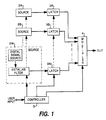
- FIGURE 1 a system for selectably multiplexing a plurality of signals is shown.
- the signal bandwidth of each of the respective signals comports with the maximum bandwidth that the channel OUT can accommodate.
- the multiplexer 4 provides a digital signal from only one of the available sources, the output signal will have the maximum available bandwidth.
- the multiplexer 4 is conditioned to time division multiplex a plurality N of the available digital signals in sample interleaved fashion, the bandwidth of the respective multiplexed signals will be reduced by the factor N, by the sampling action of the multiplexer in accordance with the Nyquest sampling criterion.
- the respective input signals applied to the multiplexer 4 must be band limited to at least one half the reciprocal of the multiplexing rate.
- a plurality of digital signal sources 2A-2N are provided.
- the respective signals may represent for example the components of a quadraphonic sound system including a monaural component, a stereo (L-R) component and the requisite additional components.
- the channel OUT may be a transmission channel.
- the multiplexer 4 will be conditioned to time division multiples 1, 2 or N of the signals.
- Each of the signal sources 2A-2N are configured similar to the element 2N, including a source of wideband digital signals coupled in cascade with an antialiasing filter.
- the antialiasing filters are responsive to a control signal provided by the controller 5.
- the control signal represents the degree of multiplexing and conditions the filters to appropriately bandlimit the information provided by the respective digital sources.
- the respective filtered signals from sources 2A-2N are coupled to respective latches 3A-3N which store the respective filtered samples for a multiplexing cycle and provide the filtered signals to respective input connections of the multiplexer 4.
- the latches 3A-3N and the multiplexer 4 are operated under the control of the controller 5. Details of the antialiasing filters will be provided hereinafter with reference to FIGURE 3.
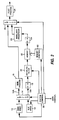
- a PIP video processor utilizing an antialiasing filter embodying the invention is illustrated.
- a PIP video processor of this type may be included in for example a television receiver (TV) or a video cassette recorder (VCR).
- main video signals and auxiliary video signals are provided by video signal sources 10 and 12 respectively.
- Sources 10 and 12 may be conventional tuners and intermediate frequency circuits which provide baseband video signals.
- the main and auxiliary video signals are coupled to respective input terminals of a switching arrangement 14, which is conditioned by the system user, via system controller 30, to apply the desired video signals to its output terminals 14A and 14B.
- the video signal applied to output terminal 14A is coupled to a main video processor 16 which may include video signal processing circuits of the type utilized ir a conventional TV receiver.
- the processed video signals from processor 16 are coupled to one input port of a further switching arrangement 26.
- Output signals from the switching arrangement 26 are coupled to a post processing circuit 28.
- the post processing circuit 28 may include driver circuits for conditioning the video signal for application to a kinescope display device.
- the post processing circuit 28 may include an r.f. modulator for providing a VHF signal.
- the video signal applied to output terminal 14B, of the switching arrangement 14, is coupled to an analog-to-digital converter (A/D) 18 which converts the analog video signal to a binary sampled data signal representing the analog signal.
- A/D analog-to-digital converter
- the binary signal provided by A/D 18 is coupled to an antialias filter 20 of the type embodied by the invention.
- Antialias filter 20 is responsive to control signals from the controller 30 to appropriately adjust the passband of the information content of the binary video signal according to the function performed by the system.
- Samples from the antialias filter 20 are coupled to a memory element 22 which may have sufficient storage capacity to store one or more frames of video signal.
- the format in which the binary signal is stored in memory element 22 is controlled by the memory controller 32 under direction from the system controller 30.
- Memory controller 32 will include memory write and read address generating circuitry.
- D/A digital-to-analog converter
- auxiliary signal processor 25 which may include circuitry for brightness and contrast control, matrixing, etc. Processed signal from the auxiliary processor 25 is coupled to a second input terminal of the switch arrangement 26.
- the switch arrangement 26 is controlled by the system controller 30 to provide various combinations of output signals to the post processor 28.
- a first mode switch arrangement 26 is conditioned to provide signal from only the main processor 16. In this mode the output signal is similar to a video signal as provided by a conventional TV receiver.
- the switch arrangement 26 may be conditioned to time division multiplex the signals from both the main and auxiliary processors in a known sequence to provide a signal conforming to a picture-in-picture video signal.
- the switch arrangement 26 may be conditioned to provide output signal from the auxiliary processor 25 only.
- image formats may be generated, according to the operation of the memory controller. For example, full resolution still images, multipicture images, zoomed images, etc., may be provided. Circuitry for generating such features, that is the configuration and/or operation of the memory controller, is known in the video signal processing arts, and therefore details will not be provided herein.
- an antialias filter or filters located before the A/D converter may include provision for bypassing the filter when full band signals are output.
- the antialias filters have a fixed passband and generally provide compromised performance of at least some of the features.
- the current arrangement, including a programmable antialias filter overcomes this shortcoming.
- the main and auxiliary video sources 10 and 12 provide composite video signals.
- the main video processor 16 and the auxiliary video processor 25 may be arranged to provide separated luminance and chrominance signal components to the switch arrangement 26.
- circuitry may be included either immediately before or after the A/D 18 to separate the luminance and chrominance components of the composite signal processed thereby.
- the luminance and chrominance components will be coupled to separate antialias filters arranged to accommodate the different bandwidths of the component signals.
- the filtered output signals from the separate antialias filters may be combined in known fashion for application to a single memory element, or applied to separate memory elements.
- the chrominance component may be demodulated into its baseband color difference components.
- the baseband color difference components due to the significantly low bandwidth of the baseband color difference components relative to the luminance signal, it may only be necessary to antialias filter the luminance component.
- composite video signal may not be directly antialias filtered in the exemplary apparatus of FIGURE 2.
- the antialias filter 20 may include provision for both vertical and horizontal filtering. Alternatively one or the other of these functions may be performed by a fixed bandwidth antialias filter positioned ahead of the A/D 18.
- FIGURE 3 illustrates one embodiment of a programmable sampled data antialias filter which is conducive to band limiting horizontal video information.
- the system of FIGURE 3 operates synchronously with the applied input samples, under the control of a clock signal F s having a frequency, f s , equal to the sample rate.
- input samples Yin (which may be luminance signal samples) are coupled to the data input terminal 300 of a D-type latch 302.
- Successive input samples are stored into latch 302 under the control of the clock signal F s .
- Successive input samples from latch 302 are applied to the minuend input terminal of a subtractive combing circuit 304.
- Output differences from combining circuit 304 are coupled to a variable scaling circuit 306.
- circuit elements 304-310 form a recursive filter. It can be shown however, that with a judicious choice of sequences of "K" factors the system will generate average values over each sequence and that the bandwidth of the averaged values is directly related to the number of samples in the sequence. For example, consider one sample per sequence and a K factor of 1. Each output sample is equal to the input sample and the signal retains its full bandwidth. Next consider two samples per sequence with reciprocating K factors of 1 and 1/2. Every second output sample will be formed of half values of the two previous samples. The information bandwidth will be approximately reduced to 1/2 of the original maximum signal bandwidth due to the averaging process, that is frequencies about f s /4 are substantially attenuated.
- each successive K factor K n K n-1 /(1+K n-1 ) (2) the sum over n samples scaled by factors K n and (1-K n ) will be equal to the sum of 1/n th each input sample, or the average of n successive samples. Note however that the intermediate output samples are not usable and only the n th output value for a sequence of n is useable.
- Table I shows possible k values for sequences of 1 to 8 corresponding to bandwidth reduction factors of 1 to 8, i.e., substantial attenuation of signal frequencies above f s/2 to f s/16 .
- the first row of K values K(A) produce exact results for the sequence terminated at any value.
- Table II illustrates several examples of K value sequencing with respect to input and output samples and therefore several subsample rates.
- the particular K values used in Table II were selected from row (K(c) of Table I.
- the number in parenthesis adjacent the letter K indicates the number of K values in a sequence.
- the rows designated O(i) indicate output samples subsampled by the factor i.
- the output values O(i) are aligned with the input sample for which the output sample is valid.
- the K factors are provided to scaling circuit 306 via the ROM 318.
- the ROM 318 is programmed at consecutive address locations with K factors representing the longest sequence (i.e., greatest subsample factor) to be implemented by the system.
- An up counter 314, is arranged to count the clock signal F s modulo n, and the counted values are coupled as address codes to the ROM 318.
- the counter 314 is conditioned to count modulo n by virtue of the comparator 316.
- Comparator 316 is arranged to compare the count values from counter 314 with a value n-1 where n is the desired modulus. Note, the reference value n-1 is used rather than n because it is assumed that the counter provides an initial count value of zero. Other known modulo n counters may be utilized.
- Output samples are derived from the FIGURE 3 apparatus from the D-type latch 312 and not from combining circuit 308.
- the signal available to latch 312 is the signal from combining circuit 308 delayed by one sample period. Every n th sample provided by combining circuit 308 is latched into the D-type latch 312 under the control of a comparator 320 which generates clock pulse each time the counter 314 initiates a new counting sequence.
- Both the subsample rate and the information bandwidth are simultaneously established by applying the single reference value which controls the counter modulus.
- the circuitry illustrated in FIGURE 4 is an antialias filter subsample system which is arranged to perform subsampling of a video signal, e.g., luminance signal, in the vertical direction.
- a video signal e.g., luminance signal
- circuit elements having the same designating numerals as elements in FIGURE 3 are similar and perform like functions.
- the apparatus of FIGURE 4 produces a horizontal line of video samples (at the input sample rate) for every n horizontal line of applied signal.
- a delay element, 410 for delaying samples by one horizontal line period is substituted for the latch 310.
- Delay element 410 receives and produces samples at the input sample rate (f s ).
- Output samples Y′ out are derived directly from the combining means 308 via the cascade connection of D-type latches 416 and 418.
- Latch 416 is clocked by the input sample rate clock F s to provide all computed sample values to the latch 418.
- Latch 418 is clocked by the input sample rate clock every n th line to provide the antialias filtered vertically subsampled output signal Y′ out .
- the counter 314 is arranged to count horizontal synchronizing pulses H s which occur at the beginning of each horizontal line interval.
- comparator 316 produces a logic one valued output signal which is coupled to the reset input terminal of counter 314 and the data input of D-type latch 412.
- the logic one valued signal applied to the counter reset terminal causes the counter to reset to zero, thereby initiating another counting sequence.
- the logic one valued output signal from comparator 316 is loaded into latch 412 by the signal H ′ s during the line interval it is generated, i.e., every n th line interval.
- Signal H ′ s may be a delayed version of the horizontal synchronizing signal generated by, for example, delaying the horizontal synchronizing signal by one sample period, or a time long enough to insure that the comparator 316 output signal has changed state following the occurrence of the horizontal synchronizing pulse.
- the latch 412 provides a logic one valued output signal every n th horizontal line period and a logic zero valued output signal during all intervening line periods.
- the input sample rate clock signal F s and the output signal from latch 412 are coupled to respective input terminals of a gate circuit 414.
- the gate circuit 414 is conditioned by the signal from latch 412 to provide the clock signal F s during every n th horizontal line period.
- the gated clock signal F s is applied to latch 418, to condition latch 418 to provide the vertically subsampled signal.
- the desired output signal is to reflect an interlaced video signal
- the clock frequency is an even or odd multiple of the chrominance subcarrier frequency
- the circuit of FIGURES 3 and 4 may be connected in cascade to provide both horizontal and vertical subsampling of a video signal.
- the frequency of the clock signal applied to circuit elements of FIGURE 4 will be equal to the frequency of the clock signal F s applied to the circuit elements of FIGURE 3 divided by n. Coupling the filters in this order reduces the number of delay stages required in delay element 410.
- delay element 410 must include sufficient stages to hold an entire line of samples. Also the frequency of the clock signal F s must be the same for both circuits.
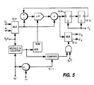
- the apparatus of FIGURE 5 is a simple variation on the circuitry of FIGURES 3 and 4 and operates in similar fashion and on the same principles.
- the sequence of scale factors K′ applied to the scaling circuit correspond to the factors (1-K) applied to the scaling circuits of FIGURES 3 and 4.
- the FIGURE 5 circuitry is arranged to filter two signals each having a sample rate of F s /2.
- the two signals U and V are time interleaved in the two-to-one multiplexer 510 and sequentially applied to the filter circuit. Respective sums for the two signals remain distinct by virtue of the two latches 516 and 518 in the feedback loop.
- the two latches are clocked at twice the input sample rate, i.e., at two times F s /2.
- Respective subsampled signals U s and V s are separated by the multiplexer 512 which is gated to select the processed samples during application of the n th K′ factor.
Landscapes
- Engineering & Computer Science (AREA)
- Multimedia (AREA)
- Signal Processing (AREA)
- Studio Circuits (AREA)
- Television Systems (AREA)
- Compression Or Coding Systems Of Tv Signals (AREA)
- Complex Calculations (AREA)
- Filters That Use Time-Delay Elements (AREA)
- Dc Digital Transmission (AREA)
- Peptides Or Proteins (AREA)
- Emergency Protection Circuit Devices (AREA)
Applications Claiming Priority (2)
| Application Number | Priority Date | Filing Date | Title |
|---|---|---|---|
| US07/301,923 US4890162A (en) | 1989-01-26 | 1989-01-26 | Adjustable antialias filters |
| US301923 | 1989-01-26 |
Publications (3)
| Publication Number | Publication Date |
|---|---|
| EP0380351A2 true EP0380351A2 (fr) | 1990-08-01 |
| EP0380351A3 EP0380351A3 (fr) | 1991-02-27 |
| EP0380351B1 EP0380351B1 (fr) | 1996-04-17 |
Family
ID=23165470
Family Applications (1)
| Application Number | Title | Priority Date | Filing Date |
|---|---|---|---|
| EP90300818A Expired - Lifetime EP0380351B1 (fr) | 1989-01-26 | 1990-01-25 | Filtres antirecouvrement ajustables |
Country Status (11)
| Country | Link |
|---|---|
| US (1) | US4890162A (fr) |
| EP (1) | EP0380351B1 (fr) |
| JP (1) | JP2715172B2 (fr) |
| KR (1) | KR0151859B1 (fr) |
| CN (1) | CN1022282C (fr) |
| DE (1) | DE69026521T2 (fr) |
| ES (1) | ES2085887T3 (fr) |
| FI (1) | FI97433C (fr) |
| MY (1) | MY104216A (fr) |
| SG (1) | SG99828A1 (fr) |
| TR (1) | TR25826A (fr) |
Cited By (39)
| Publication number | Priority date | Publication date | Assignee | Title |
|---|---|---|---|---|
| WO1997033369A3 (fr) * | 1996-02-23 | 1997-10-30 | Philips Electronics Nv | Convertisseur de signaux a complexite reduite |
| US6353735B1 (en) | 1998-10-21 | 2002-03-05 | Parkervision, Inc. | MDG method for output signal generation |
| US6370371B1 (en) | 1998-10-21 | 2002-04-09 | Parkervision, Inc. | Applications of universal frequency translation |
| US6421534B1 (en) | 1998-10-21 | 2002-07-16 | Parkervision, Inc. | Integrated frequency translation and selectivity |
| US6542722B1 (en) | 1998-10-21 | 2003-04-01 | Parkervision, Inc. | Method and system for frequency up-conversion with variety of transmitter configurations |
| US6560301B1 (en) | 1998-10-21 | 2003-05-06 | Parkervision, Inc. | Integrated frequency translation and selectivity with a variety of filter embodiments |
| US6580902B1 (en) | 1998-10-21 | 2003-06-17 | Parkervision, Inc. | Frequency translation using optimized switch structures |
| US6647250B1 (en) | 1998-10-21 | 2003-11-11 | Parkervision, Inc. | Method and system for ensuring reception of a communications signal |
| US6694128B1 (en) | 1998-08-18 | 2004-02-17 | Parkervision, Inc. | Frequency synthesizer using universal frequency translation technology |
| US6704558B1 (en) | 1999-01-22 | 2004-03-09 | Parkervision, Inc. | Image-reject down-converter and embodiments thereof, such as the family radio service |
| US6704549B1 (en) | 1999-03-03 | 2004-03-09 | Parkvision, Inc. | Multi-mode, multi-band communication system |
| US6813485B2 (en) | 1998-10-21 | 2004-11-02 | Parkervision, Inc. | Method and system for down-converting and up-converting an electromagnetic signal, and transforms for same |
| US6873836B1 (en) | 1999-03-03 | 2005-03-29 | Parkervision, Inc. | Universal platform module and methods and apparatuses relating thereto enabled by universal frequency translation technology |
| US6879817B1 (en) | 1999-04-16 | 2005-04-12 | Parkervision, Inc. | DC offset, re-radiation, and I/Q solutions using universal frequency translation technology |
| US6963734B2 (en) | 1999-12-22 | 2005-11-08 | Parkervision, Inc. | Differential frequency down-conversion using techniques of universal frequency translation technology |
| US6975848B2 (en) | 2002-06-04 | 2005-12-13 | Parkervision, Inc. | Method and apparatus for DC offset removal in a radio frequency communication channel |
| US7006805B1 (en) | 1999-01-22 | 2006-02-28 | Parker Vision, Inc. | Aliasing communication system with multi-mode and multi-band functionality and embodiments thereof, such as the family radio service |
| US7010559B2 (en) | 2000-11-14 | 2006-03-07 | Parkervision, Inc. | Method and apparatus for a parallel correlator and applications thereof |
| US7010286B2 (en) | 2000-04-14 | 2006-03-07 | Parkervision, Inc. | Apparatus, system, and method for down-converting and up-converting electromagnetic signals |
| US7027786B1 (en) | 1998-10-21 | 2006-04-11 | Parkervision, Inc. | Carrier and clock recovery using universal frequency translation |
| US7039372B1 (en) | 1998-10-21 | 2006-05-02 | Parkervision, Inc. | Method and system for frequency up-conversion with modulation embodiments |
| US7072427B2 (en) | 2001-11-09 | 2006-07-04 | Parkervision, Inc. | Method and apparatus for reducing DC offsets in a communication system |
| US7082171B1 (en) | 1999-11-24 | 2006-07-25 | Parkervision, Inc. | Phase shifting applications of universal frequency translation |
| US7085335B2 (en) | 2001-11-09 | 2006-08-01 | Parkervision, Inc. | Method and apparatus for reducing DC offsets in a communication system |
| US7110444B1 (en) | 1999-08-04 | 2006-09-19 | Parkervision, Inc. | Wireless local area network (WLAN) using universal frequency translation technology including multi-phase embodiments and circuit implementations |
| US7236754B2 (en) | 1999-08-23 | 2007-06-26 | Parkervision, Inc. | Method and system for frequency up-conversion |
| US7292835B2 (en) | 2000-01-28 | 2007-11-06 | Parkervision, Inc. | Wireless and wired cable modem applications of universal frequency translation technology |
| US7295826B1 (en) | 1998-10-21 | 2007-11-13 | Parkervision, Inc. | Integrated frequency translation and selectivity with gain control functionality, and applications thereof |
| US7321640B2 (en) | 2002-06-07 | 2008-01-22 | Parkervision, Inc. | Active polyphase inverter filter for quadrature signal generation |
| US7379883B2 (en) | 2002-07-18 | 2008-05-27 | Parkervision, Inc. | Networking methods and systems |
| US7454453B2 (en) | 2000-11-14 | 2008-11-18 | Parkervision, Inc. | Methods, systems, and computer program products for parallel correlation and applications thereof |
| US7460584B2 (en) | 2002-07-18 | 2008-12-02 | Parkervision, Inc. | Networking methods and systems |
| US7515896B1 (en) | 1998-10-21 | 2009-04-07 | Parkervision, Inc. | Method and system for down-converting an electromagnetic signal, and transforms for same, and aperture relationships |
| US7554508B2 (en) | 2000-06-09 | 2009-06-30 | Parker Vision, Inc. | Phased array antenna applications on universal frequency translation |
| US7599421B2 (en) | 1999-03-15 | 2009-10-06 | Parkervision, Inc. | Spread spectrum applications of universal frequency translation |
| US7693230B2 (en) | 1999-04-16 | 2010-04-06 | Parkervision, Inc. | Apparatus and method of differential IQ frequency up-conversion |
| US7724845B2 (en) | 1999-04-16 | 2010-05-25 | Parkervision, Inc. | Method and system for down-converting and electromagnetic signal, and transforms for same |
| US7773688B2 (en) | 1999-04-16 | 2010-08-10 | Parkervision, Inc. | Method, system, and apparatus for balanced frequency up-conversion, including circuitry to directly couple the outputs of multiple transistors |
| US8295406B1 (en) | 1999-08-04 | 2012-10-23 | Parkervision, Inc. | Universal platform module for a plurality of communication protocols |
Families Citing this family (23)
| Publication number | Priority date | Publication date | Assignee | Title |
|---|---|---|---|---|
| US5065231A (en) * | 1988-09-26 | 1991-11-12 | Apple Computer, Inc. | Apparatus and method for merging input RGB and composite video signals to provide both RGB and composite merged video outputs |
| JP3071229B2 (ja) * | 1990-04-09 | 2000-07-31 | 株式会社リコー | 図形処理装置 |
| US5107341A (en) * | 1990-04-30 | 1992-04-21 | Thompson Consumer Electronics, Inc. | Color television apparatus with picture-in-picture processing and with variable chrominance signal filtering |
| JP3122112B2 (ja) * | 1990-06-04 | 2001-01-09 | ソニー株式会社 | ビデオ信号切換装置 |
| KR960009528B1 (en) * | 1991-01-08 | 1996-07-20 | Samsung Electronics Co Ltd | 2 signal simultaneous display circuit & method through screen division |
| DE69206833T2 (de) * | 1991-02-08 | 1996-08-29 | Grass Valley Group | Gerät mit progressiver Abtastung zur Erzeugung von Fernseh-Spezialeffekten und zugehörendes Verfahren |
| US5202765A (en) * | 1991-05-06 | 1993-04-13 | Thomson Consumer Electronics, Inc. | Television receiver with picture in picture and non-linear processing |
| EP0523299A1 (fr) * | 1991-07-18 | 1993-01-20 | International Business Machines Corporation | Système et méthode pour combiner des signaux vidéo composite multiples |
| JP3158578B2 (ja) * | 1991-12-19 | 2001-04-23 | キヤノン株式会社 | 映像信号処理装置 |
| JPH05236345A (ja) * | 1992-02-21 | 1993-09-10 | Nec Ic Microcomput Syst Ltd | 画像用垂直フィルタ回路 |
| DE4231308C1 (de) * | 1992-09-18 | 1994-01-27 | Siemens Ag | Verfahren zur Bildkorrektor bei einer Bild-in-Bild-Darstellung von zeilenverkämmten Fernseh- oder Videosignalen und Schaltungsanordnung zur Durchführung desselben |
| US5361098A (en) * | 1992-11-30 | 1994-11-01 | Scientific Atlanta, Inc. | Methods and apparatus for generating a picture-in-picture digital television frame by inserting a mean-only frame into a full-size frame |
| US5933450A (en) * | 1994-04-20 | 1999-08-03 | Thomson Consumer Electronics, Inc. | Complexity determining apparatus |
| US5864583A (en) * | 1994-04-22 | 1999-01-26 | Thomson Consumer Electronics, Inc. | Parameter sampling apparatus |
| US5548341A (en) | 1994-08-05 | 1996-08-20 | Thomson Consumer Electronics, Inc. | Television receiver with non-linear processing selectively disabled during display of multi-image video signal |
| US5982453A (en) * | 1996-09-25 | 1999-11-09 | Thomson Consumer Electronics, Inc. | Reduction of visibility of spurious signals in video |
| US7072390B1 (en) | 1999-08-04 | 2006-07-04 | Parkervision, Inc. | Wireless local area network (WLAN) using universal frequency translation technology including multi-phase embodiments |
| US7054296B1 (en) | 1999-08-04 | 2006-05-30 | Parkervision, Inc. | Wireless local area network (WLAN) technology and applications including techniques of universal frequency translation |
| US6757449B1 (en) * | 1999-11-17 | 2004-06-29 | Xerox Corporation | Methods and systems for processing anti-aliased images |
| KR100471089B1 (ko) * | 2003-04-15 | 2005-03-10 | 삼성전자주식회사 | 디스플레이장치 및 그 화상처리방법 |
| TWI234398B (en) * | 2003-11-20 | 2005-06-11 | Sunplus Technology Co Ltd | Automatic contrast limiting circuit by spatial domain infinite impulse response filter and method thereof |
| JP4277071B2 (ja) * | 2006-10-20 | 2009-06-10 | Okiセミコンダクタ株式会社 | フィルタ回路 |
| US7979044B2 (en) * | 2007-09-28 | 2011-07-12 | Broadcom Corporation | Method and system for utilizing undersampling and/or a digital delay line to remove out-of-band blocker signals |
Family Cites Families (6)
| Publication number | Priority date | Publication date | Assignee | Title |
|---|---|---|---|---|
| US4064530A (en) * | 1976-11-10 | 1977-12-20 | Cbs Inc. | Noise reduction system for color television |
| US4472733A (en) * | 1982-09-01 | 1984-09-18 | Rca Corporation | Color channel signal-to-noise improvement in digital television |
| US4646138A (en) * | 1985-03-25 | 1987-02-24 | Rca Corporation | Video signal recursive filter with luma/chroma separation |
| US4656516A (en) * | 1985-03-25 | 1987-04-07 | Rca Corporation | Vertical subsampling and memory synchronization system for a picture within a picture television receiver |
| US4717951A (en) * | 1985-10-31 | 1988-01-05 | Rca Corporation | Adaptive digital filter |
| US4827343A (en) * | 1987-10-02 | 1989-05-02 | North American Philips Consumer Elec. Corp. | Method and apparatus for reducing analog/digital converter requirements in picture-in-picture television circuits |
-
1989
- 1989-01-26 US US07/301,923 patent/US4890162A/en not_active Expired - Lifetime
- 1989-09-20 MY MYPI89001289A patent/MY104216A/en unknown
-
1990
- 1990-01-19 FI FI900317A patent/FI97433C/fi not_active IP Right Cessation
- 1990-01-22 TR TR90/0108A patent/TR25826A/xx unknown
- 1990-01-23 KR KR1019900000749A patent/KR0151859B1/ko not_active Expired - Fee Related
- 1990-01-23 CN CN90100423A patent/CN1022282C/zh not_active Expired - Lifetime
- 1990-01-25 EP EP90300818A patent/EP0380351B1/fr not_active Expired - Lifetime
- 1990-01-25 JP JP2013796A patent/JP2715172B2/ja not_active Expired - Lifetime
- 1990-01-25 SG SG9602257A patent/SG99828A1/en unknown
- 1990-01-25 DE DE69026521T patent/DE69026521T2/de not_active Expired - Lifetime
- 1990-01-25 ES ES90300818T patent/ES2085887T3/es not_active Expired - Lifetime
Cited By (95)
| Publication number | Priority date | Publication date | Assignee | Title |
|---|---|---|---|---|
| WO1997033369A3 (fr) * | 1996-02-23 | 1997-10-30 | Philips Electronics Nv | Convertisseur de signaux a complexite reduite |
| US6694128B1 (en) | 1998-08-18 | 2004-02-17 | Parkervision, Inc. | Frequency synthesizer using universal frequency translation technology |
| US7376410B2 (en) | 1998-10-21 | 2008-05-20 | Parkervision, Inc. | Methods and systems for down-converting a signal using a complementary transistor structure |
| US8190116B2 (en) | 1998-10-21 | 2012-05-29 | Parker Vision, Inc. | Methods and systems for down-converting a signal using a complementary transistor structure |
| US6421534B1 (en) | 1998-10-21 | 2002-07-16 | Parkervision, Inc. | Integrated frequency translation and selectivity |
| US6542722B1 (en) | 1998-10-21 | 2003-04-01 | Parkervision, Inc. | Method and system for frequency up-conversion with variety of transmitter configurations |
| US6560301B1 (en) | 1998-10-21 | 2003-05-06 | Parkervision, Inc. | Integrated frequency translation and selectivity with a variety of filter embodiments |
| US6580902B1 (en) | 1998-10-21 | 2003-06-17 | Parkervision, Inc. | Frequency translation using optimized switch structures |
| US6647250B1 (en) | 1998-10-21 | 2003-11-11 | Parkervision, Inc. | Method and system for ensuring reception of a communications signal |
| US6687493B1 (en) | 1998-10-21 | 2004-02-03 | Parkervision, Inc. | Method and circuit for down-converting a signal using a complementary FET structure for improved dynamic range |
| US6798351B1 (en) | 1998-10-21 | 2004-09-28 | Parkervision, Inc. | Automated meter reader applications of universal frequency translation |
| US6813485B2 (en) | 1998-10-21 | 2004-11-02 | Parkervision, Inc. | Method and system for down-converting and up-converting an electromagnetic signal, and transforms for same |
| US6836650B2 (en) | 1998-10-21 | 2004-12-28 | Parkervision, Inc. | Methods and systems for down-converting electromagnetic signals, and applications thereof |
| US7697916B2 (en) | 1998-10-21 | 2010-04-13 | Parkervision, Inc. | Applications of universal frequency translation |
| US7693502B2 (en) | 1998-10-21 | 2010-04-06 | Parkervision, Inc. | Method and system for down-converting an electromagnetic signal, transforms for same, and aperture relationships |
| US7389100B2 (en) | 1998-10-21 | 2008-06-17 | Parkervision, Inc. | Method and circuit for down-converting a signal |
| US7620378B2 (en) | 1998-10-21 | 2009-11-17 | Parkervision, Inc. | Method and system for frequency up-conversion with modulation embodiments |
| US7529522B2 (en) | 1998-10-21 | 2009-05-05 | Parkervision, Inc. | Apparatus and method for communicating an input signal in polar representation |
| US7515896B1 (en) | 1998-10-21 | 2009-04-07 | Parkervision, Inc. | Method and system for down-converting an electromagnetic signal, and transforms for same, and aperture relationships |
| US8340618B2 (en) | 1998-10-21 | 2012-12-25 | Parkervision, Inc. | Method and system for down-converting an electromagnetic signal, and transforms for same, and aperture relationships |
| US7016663B2 (en) | 1998-10-21 | 2006-03-21 | Parkervision, Inc. | Applications of universal frequency translation |
| US7027786B1 (en) | 1998-10-21 | 2006-04-11 | Parkervision, Inc. | Carrier and clock recovery using universal frequency translation |
| US7039372B1 (en) | 1998-10-21 | 2006-05-02 | Parkervision, Inc. | Method and system for frequency up-conversion with modulation embodiments |
| US7050508B2 (en) | 1998-10-21 | 2006-05-23 | Parkervision, Inc. | Method and system for frequency up-conversion with a variety of transmitter configurations |
| US7826817B2 (en) | 1998-10-21 | 2010-11-02 | Parker Vision, Inc. | Applications of universal frequency translation |
| US8233855B2 (en) | 1998-10-21 | 2012-07-31 | Parkervision, Inc. | Up-conversion based on gated information signal |
| US7076011B2 (en) | 1998-10-21 | 2006-07-11 | Parkervision, Inc. | Integrated frequency translation and selectivity |
| US7865177B2 (en) | 1998-10-21 | 2011-01-04 | Parkervision, Inc. | Method and system for down-converting an electromagnetic signal, and transforms for same, and aperture relationships |
| US7936022B2 (en) | 1998-10-21 | 2011-05-03 | Parkervision, Inc. | Method and circuit for down-converting a signal |
| US7937059B2 (en) | 1998-10-21 | 2011-05-03 | Parkervision, Inc. | Converting an electromagnetic signal via sub-sampling |
| US6370371B1 (en) | 1998-10-21 | 2002-04-09 | Parkervision, Inc. | Applications of universal frequency translation |
| US8019291B2 (en) | 1998-10-21 | 2011-09-13 | Parkervision, Inc. | Method and system for frequency down-conversion and frequency up-conversion |
| US7194246B2 (en) | 1998-10-21 | 2007-03-20 | Parkervision, Inc. | Methods and systems for down-converting a signal using a complementary transistor structure |
| US7218907B2 (en) | 1998-10-21 | 2007-05-15 | Parkervision, Inc. | Method and circuit for down-converting a signal |
| US8190108B2 (en) | 1998-10-21 | 2012-05-29 | Parkervision, Inc. | Method and system for frequency up-conversion |
| US6353735B1 (en) | 1998-10-21 | 2002-03-05 | Parkervision, Inc. | MDG method for output signal generation |
| US7321735B1 (en) | 1998-10-21 | 2008-01-22 | Parkervision, Inc. | Optical down-converter using universal frequency translation technology |
| US7308242B2 (en) | 1998-10-21 | 2007-12-11 | Parkervision, Inc. | Method and system for down-converting and up-converting an electromagnetic signal, and transforms for same |
| US7245886B2 (en) | 1998-10-21 | 2007-07-17 | Parkervision, Inc. | Method and system for frequency up-conversion with modulation embodiments |
| US7295826B1 (en) | 1998-10-21 | 2007-11-13 | Parkervision, Inc. | Integrated frequency translation and selectivity with gain control functionality, and applications thereof |
| US8160534B2 (en) | 1998-10-21 | 2012-04-17 | Parkervision, Inc. | Applications of universal frequency translation |
| US6704558B1 (en) | 1999-01-22 | 2004-03-09 | Parkervision, Inc. | Image-reject down-converter and embodiments thereof, such as the family radio service |
| US7006805B1 (en) | 1999-01-22 | 2006-02-28 | Parker Vision, Inc. | Aliasing communication system with multi-mode and multi-band functionality and embodiments thereof, such as the family radio service |
| US7483686B2 (en) | 1999-03-03 | 2009-01-27 | Parkervision, Inc. | Universal platform module and methods and apparatuses relating thereto enabled by universal frequency translation technology |
| US6704549B1 (en) | 1999-03-03 | 2004-03-09 | Parkvision, Inc. | Multi-mode, multi-band communication system |
| US6873836B1 (en) | 1999-03-03 | 2005-03-29 | Parkervision, Inc. | Universal platform module and methods and apparatuses relating thereto enabled by universal frequency translation technology |
| US7599421B2 (en) | 1999-03-15 | 2009-10-06 | Parkervision, Inc. | Spread spectrum applications of universal frequency translation |
| US8229023B2 (en) | 1999-04-16 | 2012-07-24 | Parkervision, Inc. | Wireless local area network (WLAN) using universal frequency translation technology including multi-phase embodiments |
| US7539474B2 (en) | 1999-04-16 | 2009-05-26 | Parkervision, Inc. | DC offset, re-radiation, and I/Q solutions using universal frequency translation technology |
| US8223898B2 (en) | 1999-04-16 | 2012-07-17 | Parkervision, Inc. | Method and system for down-converting an electromagnetic signal, and transforms for same |
| US8224281B2 (en) | 1999-04-16 | 2012-07-17 | Parkervision, Inc. | Down-conversion of an electromagnetic signal with feedback control |
| US7929638B2 (en) | 1999-04-16 | 2011-04-19 | Parkervision, Inc. | Wireless local area network (WLAN) using universal frequency translation technology including multi-phase embodiments |
| US7894789B2 (en) | 1999-04-16 | 2011-02-22 | Parkervision, Inc. | Down-conversion of an electromagnetic signal with feedback control |
| US7272164B2 (en) | 1999-04-16 | 2007-09-18 | Parkervision, Inc. | Reducing DC offsets using spectral spreading |
| US7190941B2 (en) | 1999-04-16 | 2007-03-13 | Parkervision, Inc. | Method and apparatus for reducing DC offsets in communication systems using universal frequency translation technology |
| US7693230B2 (en) | 1999-04-16 | 2010-04-06 | Parkervision, Inc. | Apparatus and method of differential IQ frequency up-conversion |
| US8594228B2 (en) | 1999-04-16 | 2013-11-26 | Parkervision, Inc. | Apparatus and method of differential IQ frequency up-conversion |
| US6879817B1 (en) | 1999-04-16 | 2005-04-12 | Parkervision, Inc. | DC offset, re-radiation, and I/Q solutions using universal frequency translation technology |
| US8077797B2 (en) | 1999-04-16 | 2011-12-13 | Parkervision, Inc. | Method, system, and apparatus for balanced frequency up-conversion of a baseband signal |
| US8036304B2 (en) | 1999-04-16 | 2011-10-11 | Parkervision, Inc. | Apparatus and method of differential IQ frequency up-conversion |
| US7773688B2 (en) | 1999-04-16 | 2010-08-10 | Parkervision, Inc. | Method, system, and apparatus for balanced frequency up-conversion, including circuitry to directly couple the outputs of multiple transistors |
| US7224749B2 (en) | 1999-04-16 | 2007-05-29 | Parkervision, Inc. | Method and apparatus for reducing re-radiation using techniques of universal frequency translation technology |
| US7724845B2 (en) | 1999-04-16 | 2010-05-25 | Parkervision, Inc. | Method and system for down-converting and electromagnetic signal, and transforms for same |
| US7653145B2 (en) | 1999-08-04 | 2010-01-26 | Parkervision, Inc. | Wireless local area network (WLAN) using universal frequency translation technology including multi-phase embodiments and circuit implementations |
| US7110444B1 (en) | 1999-08-04 | 2006-09-19 | Parkervision, Inc. | Wireless local area network (WLAN) using universal frequency translation technology including multi-phase embodiments and circuit implementations |
| US8295406B1 (en) | 1999-08-04 | 2012-10-23 | Parkervision, Inc. | Universal platform module for a plurality of communication protocols |
| US7546096B2 (en) | 1999-08-23 | 2009-06-09 | Parkervision, Inc. | Frequency up-conversion using a harmonic generation and extraction module |
| US7236754B2 (en) | 1999-08-23 | 2007-06-26 | Parkervision, Inc. | Method and system for frequency up-conversion |
| US7082171B1 (en) | 1999-11-24 | 2006-07-25 | Parkervision, Inc. | Phase shifting applications of universal frequency translation |
| US7379515B2 (en) | 1999-11-24 | 2008-05-27 | Parkervision, Inc. | Phased array antenna applications of universal frequency translation |
| US6963734B2 (en) | 1999-12-22 | 2005-11-08 | Parkervision, Inc. | Differential frequency down-conversion using techniques of universal frequency translation technology |
| US7292835B2 (en) | 2000-01-28 | 2007-11-06 | Parkervision, Inc. | Wireless and wired cable modem applications of universal frequency translation technology |
| US7496342B2 (en) | 2000-04-14 | 2009-02-24 | Parkervision, Inc. | Down-converting electromagnetic signals, including controlled discharge of capacitors |
| US7822401B2 (en) | 2000-04-14 | 2010-10-26 | Parkervision, Inc. | Apparatus and method for down-converting electromagnetic signals by controlled charging and discharging of a capacitor |
| US7010286B2 (en) | 2000-04-14 | 2006-03-07 | Parkervision, Inc. | Apparatus, system, and method for down-converting and up-converting electromagnetic signals |
| US8295800B2 (en) | 2000-04-14 | 2012-10-23 | Parkervision, Inc. | Apparatus and method for down-converting electromagnetic signals by controlled charging and discharging of a capacitor |
| US7386292B2 (en) | 2000-04-14 | 2008-06-10 | Parkervision, Inc. | Apparatus, system, and method for down-converting and up-converting electromagnetic signals |
| US7107028B2 (en) | 2000-04-14 | 2006-09-12 | Parkervision, Inc. | Apparatus, system, and method for up converting electromagnetic signals |
| US7218899B2 (en) | 2000-04-14 | 2007-05-15 | Parkervision, Inc. | Apparatus, system, and method for up-converting electromagnetic signals |
| US7554508B2 (en) | 2000-06-09 | 2009-06-30 | Parker Vision, Inc. | Phased array antenna applications on universal frequency translation |
| US7233969B2 (en) | 2000-11-14 | 2007-06-19 | Parkervision, Inc. | Method and apparatus for a parallel correlator and applications thereof |
| US7991815B2 (en) | 2000-11-14 | 2011-08-02 | Parkervision, Inc. | Methods, systems, and computer program products for parallel correlation and applications thereof |
| US7454453B2 (en) | 2000-11-14 | 2008-11-18 | Parkervision, Inc. | Methods, systems, and computer program products for parallel correlation and applications thereof |
| US7433910B2 (en) | 2000-11-14 | 2008-10-07 | Parkervision, Inc. | Method and apparatus for the parallel correlator and applications thereof |
| US7010559B2 (en) | 2000-11-14 | 2006-03-07 | Parkervision, Inc. | Method and apparatus for a parallel correlator and applications thereof |
| US7653158B2 (en) | 2001-11-09 | 2010-01-26 | Parkervision, Inc. | Gain control in a communication channel |
| US8446994B2 (en) | 2001-11-09 | 2013-05-21 | Parkervision, Inc. | Gain control in a communication channel |
| US7085335B2 (en) | 2001-11-09 | 2006-08-01 | Parkervision, Inc. | Method and apparatus for reducing DC offsets in a communication system |
| US7072427B2 (en) | 2001-11-09 | 2006-07-04 | Parkervision, Inc. | Method and apparatus for reducing DC offsets in a communication system |
| US6975848B2 (en) | 2002-06-04 | 2005-12-13 | Parkervision, Inc. | Method and apparatus for DC offset removal in a radio frequency communication channel |
| US7321640B2 (en) | 2002-06-07 | 2008-01-22 | Parkervision, Inc. | Active polyphase inverter filter for quadrature signal generation |
| US8160196B2 (en) | 2002-07-18 | 2012-04-17 | Parkervision, Inc. | Networking methods and systems |
| US8407061B2 (en) | 2002-07-18 | 2013-03-26 | Parkervision, Inc. | Networking methods and systems |
| US7379883B2 (en) | 2002-07-18 | 2008-05-27 | Parkervision, Inc. | Networking methods and systems |
| US7460584B2 (en) | 2002-07-18 | 2008-12-02 | Parkervision, Inc. | Networking methods and systems |
Also Published As
| Publication number | Publication date |
|---|---|
| CN1044744A (zh) | 1990-08-15 |
| FI97433B (fi) | 1996-08-30 |
| CN1022282C (zh) | 1993-09-29 |
| TR25826A (tr) | 1993-09-01 |
| EP0380351A3 (fr) | 1991-02-27 |
| KR900012423A (ko) | 1990-08-04 |
| JPH02237305A (ja) | 1990-09-19 |
| US4890162A (en) | 1989-12-26 |
| KR0151859B1 (ko) | 1998-12-15 |
| SG99828A1 (en) | 2003-11-27 |
| EP0380351B1 (fr) | 1996-04-17 |
| FI97433C (fi) | 1996-12-10 |
| ES2085887T3 (es) | 1996-06-16 |
| JP2715172B2 (ja) | 1998-02-18 |
| DE69026521D1 (de) | 1996-05-23 |
| MY104216A (en) | 1994-02-28 |
| DE69026521T2 (de) | 1996-11-21 |
| FI900317A0 (fi) | 1990-01-19 |
Similar Documents
| Publication | Publication Date | Title |
|---|---|---|
| EP0380351B1 (fr) | Filtres antirecouvrement ajustables | |
| EP0821858B1 (fr) | Filtre luminance-chrominance a element de temporisation commun | |
| EP0391094B1 (fr) | Dispositif de doublage de lignes de balayage de télévision avec un filtre de valeur moyenne temporelle | |
| EP0196826B1 (fr) | Système de filtrage pour traitement d'une image vidéo de définition réduite | |
| TW214030B (fr) | ||
| EP0322955A1 (fr) | Traitement de signaux sous-échantillonnés | |
| KR960006532B1 (ko) | 텔레비젼 신호 처리 회로 | |
| CA1250657A (fr) | Systeme filtrant adaptatif | |
| JPS6242692A (ja) | テレビジヨン信号の原色アナログ信号を発生する回路 | |
| KR940011030B1 (ko) | 필터링 시스템을 갖는 합성 신호 처리 장치 | |
| US5136379A (en) | Video signal processing device capable of vertical blocking | |
| EP0065881B1 (fr) | Système pour le filtrage de signaux de télévision | |
| EP0276985B1 (fr) | Traitement vidéo | |
| GB2111340A (en) | Digital chrominance filter for digital component television system | |
| EP0690632A1 (fr) | Décodeur numérique pour signaux vidéo et méthode de décodage numérique de signal vidéo | |
| US4682227A (en) | Digital video signal processing apparatus for providing zoom and compressive images with soft focus | |
| US5159437A (en) | Television signal converting apparatus | |
| EP0150098B1 (fr) | Systèmes de traitement numérique de la luminance | |
| EP0309976B1 (fr) | Agencement de circuit pour le traitement de composantes vidéo | |
| GB2181321A (en) | Video signal processing and display system | |
| KR0140246B1 (ko) | Muse/ntsc 방식 신호변환방법 및 그 장치 | |
| KR0147559B1 (ko) | 16:9의 맥 화면을 4:3 수상기로 보기위한 샘플보간회로 | |
| CN1140375A (zh) | 用于盒式磁带录像机的双画面产生装置 | |
| JP2768730B2 (ja) | ハイビジョン受信装置 | |
| CZ316991A3 (en) | wide-screen television display |
Legal Events
| Date | Code | Title | Description |
|---|---|---|---|
| PUAI | Public reference made under article 153(3) epc to a published international application that has entered the european phase |
Free format text: ORIGINAL CODE: 0009012 |
|
| AK | Designated contracting states |
Kind code of ref document: A2 Designated state(s): AT DE ES FR GB IT |
|
| PUAL | Search report despatched |
Free format text: ORIGINAL CODE: 0009013 |
|
| AK | Designated contracting states |
Kind code of ref document: A3 Designated state(s): AT DE ES FR GB IT |
|
| 17P | Request for examination filed |
Effective date: 19910806 |
|
| RAP1 | Party data changed (applicant data changed or rights of an application transferred) |
Owner name: RCA THOMSON LICENSING CORPORATION |
|
| 17Q | First examination report despatched |
Effective date: 19931203 |
|
| RBV | Designated contracting states (corrected) |
Designated state(s): DE ES FR GB IT |
|
| GRAH | Despatch of communication of intention to grant a patent |
Free format text: ORIGINAL CODE: EPIDOS IGRA |
|
| GRAA | (expected) grant |
Free format text: ORIGINAL CODE: 0009210 |
|
| AK | Designated contracting states |
Kind code of ref document: B1 Designated state(s): DE ES FR GB IT |
|
| REF | Corresponds to: |
Ref document number: 69026521 Country of ref document: DE Date of ref document: 19960523 |
|
| ET | Fr: translation filed | ||
| REG | Reference to a national code |
Ref country code: ES Ref legal event code: FG2A Ref document number: 2085887 Country of ref document: ES Kind code of ref document: T3 |
|
| ITF | It: translation for a ep patent filed | ||
| PLBE | No opposition filed within time limit |
Free format text: ORIGINAL CODE: 0009261 |
|
| STAA | Information on the status of an ep patent application or granted ep patent |
Free format text: STATUS: NO OPPOSITION FILED WITHIN TIME LIMIT |
|
| 26N | No opposition filed | ||
| REG | Reference to a national code |
Ref country code: GB Ref legal event code: 732E |
|
| REG | Reference to a national code |
Ref country code: GB Ref legal event code: IF02 |
|
| REG | Reference to a national code |
Ref country code: FR Ref legal event code: D6 |
|
| REG | Reference to a national code |
Ref country code: GB Ref legal event code: 746 Effective date: 20030228 |
|
| PGFP | Annual fee paid to national office [announced via postgrant information from national office to epo] |
Ref country code: IT Payment date: 20060131 Year of fee payment: 17 |
|
| PGFP | Annual fee paid to national office [announced via postgrant information from national office to epo] |
Ref country code: ES Payment date: 20070131 Year of fee payment: 18 |
|
| REG | Reference to a national code |
Ref country code: ES Ref legal event code: FD2A Effective date: 20080126 |
|
| PGFP | Annual fee paid to national office [announced via postgrant information from national office to epo] |
Ref country code: DE Payment date: 20090120 Year of fee payment: 20 |
|
| PGFP | Annual fee paid to national office [announced via postgrant information from national office to epo] |
Ref country code: GB Payment date: 20081230 Year of fee payment: 20 |
|
| PG25 | Lapsed in a contracting state [announced via postgrant information from national office to epo] |
Ref country code: ES Free format text: LAPSE BECAUSE OF NON-PAYMENT OF DUE FEES Effective date: 20080126 |
|
| PG25 | Lapsed in a contracting state [announced via postgrant information from national office to epo] |
Ref country code: IT Free format text: LAPSE BECAUSE OF NON-PAYMENT OF DUE FEES Effective date: 20070125 |
|
| PGFP | Annual fee paid to national office [announced via postgrant information from national office to epo] |
Ref country code: FR Payment date: 20090123 Year of fee payment: 20 |
|
| REG | Reference to a national code |
Ref country code: GB Ref legal event code: PE20 Expiry date: 20100124 |
|
| PG25 | Lapsed in a contracting state [announced via postgrant information from national office to epo] |
Ref country code: GB Free format text: LAPSE BECAUSE OF EXPIRATION OF PROTECTION Effective date: 20100124 |
|
| PG25 | Lapsed in a contracting state [announced via postgrant information from national office to epo] |
Ref country code: DE Free format text: LAPSE BECAUSE OF EXPIRATION OF PROTECTION Effective date: 20100125 |