EP0381064A2 - Mécanisme d'adressage pour accéder en parallèle à plusieurs positions voisines à partir d'une mémoire plein champ - Google Patents
Mécanisme d'adressage pour accéder en parallèle à plusieurs positions voisines à partir d'une mémoire plein champ Download PDFInfo
- Publication number
- EP0381064A2 EP0381064A2 EP90101551A EP90101551A EP0381064A2 EP 0381064 A2 EP0381064 A2 EP 0381064A2 EP 90101551 A EP90101551 A EP 90101551A EP 90101551 A EP90101551 A EP 90101551A EP 0381064 A2 EP0381064 A2 EP 0381064A2
- Authority
- EP
- European Patent Office
- Prior art keywords
- data
- full field
- field memory
- address
- pixels
- Prior art date
- Legal status (The legal status is an assumption and is not a legal conclusion. Google has not performed a legal analysis and makes no representation as to the accuracy of the status listed.)
- Withdrawn
Links
Images

Classifications
-
- G—PHYSICS
- G06—COMPUTING OR CALCULATING; COUNTING
- G06T—IMAGE DATA PROCESSING OR GENERATION, IN GENERAL
- G06T1/00—General purpose image data processing
- G06T1/60—Memory management
Definitions
- This invention relates generally to data processing for graphic display systems and, more particularly, to an addressing mechanism for accessing multiple neighboring locations from full field memory in parallel in order to simplify bi-linear interpolation data accessing during rotation and scaling of raster images in a digital map, radar or other digitized video system.
- avionics displays have been designed to display aeronautical charts and other information to an aircraft pilot.
- the information displayed is generated from a digital data base and is referred to as a "digital map".
- the invention as characterized in the independent claims reduces the required memory space and the processing time.
- the full field memory is divided into four quarters. Each quarter has its own address and data bus.
- the controlling logic modifies the incoming X,Y addresses to access the corner which is contained in its addressing space.
- the four data buses then must be rearranged such that the four pixels are output on the appropriate corner positions for the bi-linear interpolator. In this application, the four corners are ordered from left to right and top to bottom.
- the invention also detects address overflow to blank pixels which are outside of the addressing space.
- the invention allows serial data input modes while generating the addressing for such modes.
- the input and output modes can also be reversed such that four corners can be written in parallel while the readout modes would be strictly serial. This feature is useful for anti-aliasing or automatic line doubling. Further improvements and modifications of the invention are described in the dependent claims.
- An apparatus for accessing a plurality of neighboring pixel locations from a full field memory in parallel comprises means for dividing the full field memory into sections wherein each section has an address and data bus; means for modifying incoming X,Y addresses to access the screen location which is contained in its addressing space and means for arranging the data buses so as to cause the plurality of pixels to be output on the appropriate screen location positions wherein the dividing means, modifying means and arranging means cooperate to process the data so that the plurality of neighboring pixel locations are output in parallel and in a predetermined arrangement.
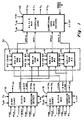
- FIG. 1 one example of an embodiment of the invention is shown schematically in block diagram form.
- This particular embodiment processes radar video data but can easily handle digital map or other types of digitized video data.
- the embodiment shown in Figure 1 includes address control chips 10 and 12, full field memory 30 and data control chip 22.
- the full field memory 30 is organized into sections wherein each section comprises a random access memory (RAM) having an equal share of the total memory locations.
- RAM random access memory
- the full field memory 30 may be organized into four 256x256x4 memory areas, each of which may be represented by a single 64kx4 RAM.
- each area is interleaved by the least significant bits (LSBs) of X and Y.
- LSBs least significant bits
- the 64kx4 RAM chosen for a particular address is determined by the LSB of X and Y as shown in Table I below.
- the address to each 64kx4 RAM is taken from X bits 1-8 and Y bits 1-8, with the LSB (bit 0) of X,Y being used to do the chip selection.
- MSB most significant bit
- bit 9 is not used during writing; however, in the readout modes it detects the off-screen accesses (X,Y OVF).
- address control chip 10 includes inputs PING, RCLK, X RESET, X INC, X DEC, WS, YLSB and XS.
- address control chip 12 has inputs PING, RCLK, Y, Y RESET, Y INC, Y DEC, WS, Y OVF.
- Both address control chips include a 10-bit counter, a 2x2x8 multiplexer and overflow detection capabilities.
- the address control chips for X and Y, 10 and 12, respectively, are functionally equivalent and could be implemented, for example, in a pair of gate arrays or with discrete logic elements. The minor differences between the two address chips could be advantageously controlled by the XS (X select) line.
- the X address control chip 10 does read/strobe and chip select for RAM0 and RAM1 and the Y address control chip 12 performs write/strobe and chip selects for RAM2 and RAM3.
- Outputs for address control chip 10 include XLSB, X OVF, X EVEN, R/S, X ODD, CS0 and CS1.
- Address control chip 12 includes outputs Y EVEN, Y ODD, CS2, CS3, YLSB, W/S and Y OVF.
- PING is a logical signal which activates the address control chips 10 and 12. Since PING is equal to the inverse of PONG, one part of the scene memory can be updated while the other is being scanned by the readout function. Thus, while one FFM is in a readout mode (PONG), the other is in the data reception mode (PING).
- RCLK is the read clock control for the data processing circuitry shown in Figure 1. This may be, for example, the same clock which is synchronized to the radar video input circuitry (not shown).
- X is a 10 bit bus which carries the address data for the X coordinate.
- Y in address control chip 12 carries the 10 bit address data for the Y coordinate.
- X RESET is a reset line which is activated by an external signal, supplied, for example, by a printed circuit board which interfaces with a radar system. Similarly, Y RESET resets the Y address data chip 12.
- X INC is an externally generated signal which commands the X address chip 10 to increment X. Similarly, Y INC causes the Y address data chip 12 to increment Y.
- X DEC and Y DEC operate upon activation to decrement the X and Y addresses, respectively.
- W/S for both chips 10 and 12 is the control signal for a read/strobe (R/S) in the case of chip 10 and a write/strobe (W/S) in the case of chip 12.
- R/S read/strobe
- W/S write/strobe
- the X select or XS signals choose which set of data causes the chip selects, CS0, CS1, CS2, and CS3 to be designated from the X or Y address control chips.
- the RAMs which comprise the FFM 30 are controlled by chip selects CS0-CS3 and have read/strobe and write/strobe inputs as well as bidirectional buses connecting the RAMs to the data control chip 22.
- Address control chip 10 is connected to RAM0 14 and RAM2 18 by means of the X EVEN bus.
- the X EVEN bus is an 8 bit bus in this example.
- Address control chip 10 is connected to RAM1 16 and RAM3 20 by means of the X ODD bus which is also an 8 bit bus.
- X EVEN and X ODD carry X bits 1-8.
- Address control chip 12 is connected to RAM0 14 and RAM1 16 through the Y EVEN bus. Connections to RAM2 18 and RAM3 20 are made through the Y ODD bus.
- Both Y EVEN and Y ODD advantageously comprise 8 bit buses carrying Y bits 1-8.
- the data control chip 22 includes the bidirectional, 4 bit buses DATA 0-DATA 3 connected to RAM0-RAM3 in parallel. Other inputs include X,Y OVF and RADAR VIDEO IN. Data control chip 22 further may comprise a 4x4x4 multiplexer with a zero overflow capability as well as bidirectional data bus drivers. Outputs include 4 bit buses I0, I1, I2 and I3. I0-I3 are preferably 4 bit parallel readout buses wherein the I0 output must always be in the upper left corner of the display, I1 the upper right corner, I2 the lower left corner and I3 the lower right corner.
- data is received at the RADAR VIDEO IN line from electronics associated with a radar system in, for example, an aircraft (not shown), at the pixel rate of digitization which may typically be 512 pixels per raster line.
- Control signals needed to operate the 10 bit counters within the address control chips 10 and 12 are also generated externally.
- the 10 bit counters inherent in the address control chips 10 and 12 will generate the X and Y addresses which are subsequently sent to the FFM. Y will be reset at the start of a vertical scan and incremented once for odd frames, then X will be reset at the start of each line.
- X is then incremented once per digitization or decremented for alternate lines depending on the scan mode being implemented by the video readout system. At the end of each line, Y is incremented twice to account for interlacing.
- the write/strobe signal (W/S) is clocked once for each pixel after allowing for setup times.
- the data control chip 22 is set to route the radar video signal directly to all four 64kx4 RAM data buses.
- the address control chips 10 and 12 then control the chip selects CS0-CS3 to insure only the proper RAM is written into.
- the X address control chip 10 does read/strobe and chip selects CS0 and CS1 and the Y address control chip 12 performs write/strobe and chip selects CS2 and CS3.
- One important aspect of the invention is the ability to output in parallel the four pixels which surround the desired fractional readout point for bi-linear interpolation which may be carried out downstream of the scene memory block shown in Figure 1.
- the full field memory is set up to accommodate this requirement by outputting the four adjacent pixels when given the X,Y coordinate of the upper left corner (for example, X,Y integer position).
- the read clock (RCLK) goes active, all four RAMs are enabled to output their data, but the address to each chip is potentially different according to Table II.
- the four overflow bits (MSB of X,X+1,Y,Y+1) must be considered such that 0 is output if an address is out of the valid FFM bounds.
- the valid FFM bounds are application specific and are predetermined in a manner well known in the art.
- the blanking function is controlled as shown in Table IV hereinbelow. TABLE IV NON-ZERO BIT OUTPUTS BLANKED X MSB I0,I2 X+1 MSB I1,I3 Y MSB I0,I1 Y+1 MSB I2,I3
- Figure 2 is a pictorial representation of Table III.
- UL designates the upper left pixel
- UR designates the upper right pixel
- LL designates the lower left pixel
- LR designates the lower right pixel.
- Figure 3 shows in block diagram form a schematic representation of the X data multiplexing scheme of the invention.
- Registers 40, 42, 44 and 46 would be contained internal to X address control chip 10 in a preferred embodiment of the invention.
- the least significant bit or "0" bit of X would be routed to the XLSB ENABLE line shown.
- the X data would be routed to the X EVEN bus or the X ODD bus.
- Registers 40 and 46 would contain data corresponding to the address for X while registers 42 and 44 would contain the address X+1.
- the Y address control chip 12 operates in a similar manner routing the Y and Y+1 addresses according to the value of YLSB. Thus, the multiplexing as shown in Table III and Figure 2 is accomplished.
- the RAM memories may be any memories which operate in the range of about 80 to 90 nanoseconds. Utilizing the teachings of the invention, this would allow reading of four neighboring pixels in about 109 nanoseconds which, if done in series form, would require super fast, very expensive RAMs.
- the data control chip and address control chips may advantageously be implemented in semiconductor form. Circuitry embodying both the PING and PONG sides of scene memory would most advantageously be a two-sided, multi-layered printed circuit board having one side for PING FFM, the other side for PONG FFM.
- the address scheme of the invention for other applications that require the interlacing of less than four pixels or more than four pixels and wherein the positions are ordered according to a predetermined scheme based upon screen location of the pixels other than four corners.
- the addressing scheme of the invention may be used in applications where the data is not representative of pixels for a graphic display, but may represent other types of data.
- Alternative embodiments of the invention could write data into memory by assigning X and Y addresses so as to correspond to the screen location which is contained in the memory's addressing space according to a multiplexing scheme based upon the values of the least significant bits of X and Y.
- the flow of the multiplexing scheme shown in Figure 2 would be reversed.
- the configuration shown in Figures 1 and 2 could be layered advantageously to be adapted to access or write a matrix of neighboring pixels, such as a four-by-four matrix. In such a layered configuration, the number of elements would obviously be doubled with both X and Y having four data paths each.
- the full field memory would consist of sixteen memory sets instead of four. Expansion of the principles of the invention to larger matrixes would merely require the addition of more layers of the circuitry shown in Figures 1, 2 and 3.
Landscapes
- Physics & Mathematics (AREA)
- General Physics & Mathematics (AREA)
- Engineering & Computer Science (AREA)
- Theoretical Computer Science (AREA)
- Image Input (AREA)
- Controls And Circuits For Display Device (AREA)
- Digital Computer Display Output (AREA)
Applications Claiming Priority (2)
| Application Number | Priority Date | Filing Date | Title |
|---|---|---|---|
| US30314889A | 1989-01-30 | 1989-01-30 | |
| US303148 | 1989-01-30 |
Publications (2)
| Publication Number | Publication Date |
|---|---|
| EP0381064A2 true EP0381064A2 (fr) | 1990-08-08 |
| EP0381064A3 EP0381064A3 (fr) | 1992-03-25 |
Family
ID=23170737
Family Applications (1)
| Application Number | Title | Priority Date | Filing Date |
|---|---|---|---|
| EP19900101551 Withdrawn EP0381064A3 (fr) | 1989-01-30 | 1990-01-26 | Mécanisme d'adressage pour accéder en parallèle à plusieurs positions voisines à partir d'une mémoire plein champ |
Country Status (2)
| Country | Link |
|---|---|
| EP (1) | EP0381064A3 (fr) |
| JP (1) | JPH03196376A (fr) |
Cited By (1)
| Publication number | Priority date | Publication date | Assignee | Title |
|---|---|---|---|---|
| EP0386881A3 (fr) * | 1989-03-07 | 1991-11-21 | Sony Corporation | Obtention d'accès à une portion à deux dimensions d'un signal d'image numérisée |
Families Citing this family (3)
| Publication number | Priority date | Publication date | Assignee | Title |
|---|---|---|---|---|
| JP4506256B2 (ja) * | 2004-04-19 | 2010-07-21 | ソニー株式会社 | データ格納装置、データ格納制御装置、データ格納制御方法及びデータ格納制御プログラム |
| JP4538737B2 (ja) * | 2005-04-28 | 2010-09-08 | ソニー株式会社 | データアクセス装置、データアクセス方法、プログラムおよび記録媒体 |
| JP2007249791A (ja) * | 2006-03-17 | 2007-09-27 | Sony Corp | 画像処理装置および画像処理方法、並びにプログラム |
Family Cites Families (3)
| Publication number | Priority date | Publication date | Assignee | Title |
|---|---|---|---|---|
| JPS56140390A (en) * | 1980-04-04 | 1981-11-02 | Nippon Electric Co | Picture memory |
| JPS6247786A (ja) * | 1985-08-27 | 1987-03-02 | Hamamatsu Photonics Kk | 近傍画像処理専用メモリ |
| JPS63205778A (ja) * | 1987-02-20 | 1988-08-25 | Sumitomo Electric Ind Ltd | ビデオ信号デイジタル化回路 |
-
1990
- 1990-01-26 EP EP19900101551 patent/EP0381064A3/fr not_active Withdrawn
- 1990-01-30 JP JP1811990A patent/JPH03196376A/ja active Pending
Cited By (2)
| Publication number | Priority date | Publication date | Assignee | Title |
|---|---|---|---|---|
| EP0386881A3 (fr) * | 1989-03-07 | 1991-11-21 | Sony Corporation | Obtention d'accès à une portion à deux dimensions d'un signal d'image numérisée |
| US5125048A (en) * | 1989-03-07 | 1992-06-23 | Sony Corporation | Obtaining access to a two-dimensional portion of a digital picture signal |
Also Published As
| Publication number | Publication date |
|---|---|
| JPH03196376A (ja) | 1991-08-27 |
| EP0381064A3 (fr) | 1992-03-25 |
Similar Documents
| Publication | Publication Date | Title |
|---|---|---|
| CA1122696A (fr) | Appareil rotateur d'images | |
| US5062057A (en) | Computer display controller with reconfigurable frame buffer memory | |
| JP2558236B2 (ja) | 画像変換メモリ装置 | |
| US5742788A (en) | Method and apparatus for providing a configurable display memory for single buffered and double buffered application programs to be run singly or simultaneously | |
| US4878117A (en) | Video signal mixing unit for simultaneously displaying video signals having different picture aspect ratios and resolutions | |
| KR900005297B1 (ko) | 화상메모리 주변장치 | |
| EP0737956B1 (fr) | Mémoire de trame pour des données graphiques | |
| EP0139095A2 (fr) | Sélection d'image dans un dispositif d'affichage à balayage à trame | |
| EP0704824A2 (fr) | Organisation de mémoire d'étiquettes de tampon Z | |
| US4845640A (en) | High-speed dual mode graphics memory | |
| EP0480564B1 (fr) | Améliorations d'un affichage à balaye de trame | |
| EP0361739A2 (fr) | Appareil de balayage pour lire une image | |
| US4847691A (en) | Processing of video image signals | |
| EP0381064A2 (fr) | Mécanisme d'adressage pour accéder en parallèle à plusieurs positions voisines à partir d'une mémoire plein champ | |
| EP0431581A2 (fr) | Méthode et dispositif pour changer l'orientation d'un dispositif d'affichage vidéo | |
| US5657047A (en) | Method and apparatus for zooming images on a video display | |
| EP0589724B1 (fr) | Système et méthode électronique de traitement d'images | |
| JPH04228180A (ja) | ランダムアクセスポートおよびシリアルアクセスポートを有するメモリアレイ | |
| US5287451A (en) | Method of presenting images on a hardware screen and a system for implementing the method | |
| US5083121A (en) | System for maximizing utilization of a display memory | |
| US5519413A (en) | Method and apparatus for concurrently scanning and filling a memory | |
| US6046753A (en) | Electronic image processing system for modifying initial image data | |
| EP0231780B1 (fr) | Circuit de traitement de vecteurs pour un dispositif d'affichage à mémoire cartographique | |
| US4766496A (en) | Video signal memories | |
| JPH0588665A (ja) | 画像表示制御装置 |
Legal Events
| Date | Code | Title | Description |
|---|---|---|---|
| PUAI | Public reference made under article 153(3) epc to a published international application that has entered the european phase |
Free format text: ORIGINAL CODE: 0009012 |
|
| AK | Designated contracting states |
Kind code of ref document: A2 Designated state(s): DE FR GB IT |
|
| PUAL | Search report despatched |
Free format text: ORIGINAL CODE: 0009013 |
|
| AK | Designated contracting states |
Kind code of ref document: A3 Designated state(s): DE FR GB IT |
|
| STAA | Information on the status of an ep patent application or granted ep patent |
Free format text: STATUS: THE APPLICATION IS DEEMED TO BE WITHDRAWN |
|
| 18D | Application deemed to be withdrawn |
Effective date: 19920801 |