EP0381067A2 - Méthode d'enregistrement de modèle C.A.D. sur des images vidéo avec addition de fouillis - Google Patents
Méthode d'enregistrement de modèle C.A.D. sur des images vidéo avec addition de fouillis Download PDFInfo
- Publication number
- EP0381067A2 EP0381067A2 EP90101560A EP90101560A EP0381067A2 EP 0381067 A2 EP0381067 A2 EP 0381067A2 EP 90101560 A EP90101560 A EP 90101560A EP 90101560 A EP90101560 A EP 90101560A EP 0381067 A2 EP0381067 A2 EP 0381067A2
- Authority
- EP
- European Patent Office
- Prior art keywords
- image
- cad
- filtered
- filtering
- correlating
- Prior art date
- Legal status (The legal status is an assumption and is not a legal conclusion. Google has not performed a legal analysis and makes no representation as to the accuracy of the status listed.)
- Withdrawn
Links
Images


Classifications
-
- G—PHYSICS
- G06—COMPUTING OR CALCULATING; COUNTING
- G06T—IMAGE DATA PROCESSING OR GENERATION, IN GENERAL
- G06T7/00—Image analysis
- G06T7/30—Determination of transform parameters for the alignment of images, i.e. image registration
- G06T7/32—Determination of transform parameters for the alignment of images, i.e. image registration using correlation-based methods
-
- G—PHYSICS
- G06—COMPUTING OR CALCULATING; COUNTING
- G06T—IMAGE DATA PROCESSING OR GENERATION, IN GENERAL
- G06T7/00—Image analysis
- G06T7/70—Determining position or orientation of objects or cameras
- G06T7/73—Determining position or orientation of objects or cameras using feature-based methods
- G06T7/74—Determining position or orientation of objects or cameras using feature-based methods involving reference images or patches
-
- G—PHYSICS
- G06—COMPUTING OR CALCULATING; COUNTING
- G06V—IMAGE OR VIDEO RECOGNITION OR UNDERSTANDING
- G06V10/00—Arrangements for image or video recognition or understanding
- G06V10/20—Image preprocessing
- G06V10/24—Aligning, centring, orientation detection or correction of the image
-
- G—PHYSICS
- G06—COMPUTING OR CALCULATING; COUNTING
- G06V—IMAGE OR VIDEO RECOGNITION OR UNDERSTANDING
- G06V2201/00—Indexing scheme relating to image or video recognition or understanding
- G06V2201/06—Recognition of objects for industrial automation
Definitions
- Image matching has its roots in research on binocular stereo, where correspondences between a pair of images must be found to compute range from parallax. Two principal approaches have been followed in prior research to solve the stereo correspondence problem--area correlation techniques applied to intensity images, and symbolic feature matching techniques.
- Intensity based area-correlation techniques have been the principal technique used for commercial applications in stereo-photogrammetry.
- a principal advantage of area-correlation is its simplicity. This makes modelling and interpreting the behavior of such a system easier and it also makes high performance implementations practical.
- Intensity correlation has several drawbacks.
- the correlation is sensitive to absolute intensity levels, which means that correlation levels cannot be used directly as a confidence measure.
- intensity gradients in the images give rise to gradients in the correlation surface which can bias peak locations and in severe cases can completely mask the true correlation peak.
- Nishihara developed an area correlation algorithm that avoided these pitfalls by applying the correlation to a binary representation. This idea was derived from research on symbolic feature matching approaches. His sign correlation approach gives essentially the same results as earlier approaches when noise levels are low, but its behavior differs significantly at high noise levels where it continues to give a defined match. This is reported at H.K. Nishihara, "Practical Real Time Imaging Stereo Matcher,” Opt. Eng., vol. 23, no. 5, pp 536-545 (1984).
- the problem of measuring binocular disparity between a stereo pair of images would seem to relate to the problem of registering an image to a CAD model.
- relative position disparities are measured between corresponding regions in the stereo pair.
- the objective is to measure the translation disparity between an image of a real device and a synthetic image generated from the CAD data used to make the device.
- the CAD problem differs from the stereo problem in a very significant way.
- the two stereo images are qualitatively the same, and tend to contain the same level of information. Put colloquially, they are both apples.
- the actual image of a device, and the synthetic binary image of the database used to make the device are very different.
- the device image contains geometrical and optical artifacts that tend to mask the structure; furthermore the device image contains additional information such as other visible layers in an integrated circuit (“IC”) chip.
- IC integrated circuit
- the present invention provides a simple technique for position-finding on a manufactured device such as an integrated circuit ("IC”) or a printed circuit board (“PCB”), relating the observed image to a description such as the CAD database that was used to create the devices.
- IC integrated circuit
- PCB printed circuit board
- the technique requires few adjustments and provides useful results, even in the presence of large amounts of noise or other features present in the image but not represented in the database.
- the invention contemplates providing an optical image of the surface of the device, obtained with an imaging device such as a video camera and a microscope, generating a synthetic CAD image from the CAD database, subjecting both images to a filtering operation (Laplacian of Gaussian convolution), binarizing (taking the sign of) the results, and correlating the two filtered and binarized images (referred to as "processed" images) to determine relative alignment.
- a filtering operation Laplacian of Gaussian convolution
- binarizing taking the sign of
- correlating the two filtered and binarized images referred to as "processed” images
- One application of the invention is to allow precision positioning of a positioning head relative to a workpiece.
- An example would be placing an IC device on a PCB.
- a positioning head to which a camera is mounted is driven to the approximate location of the IC site by a positioning mechanism.
- the positioning mechanism need not be accurate for large increments of travel, but must be capable of providing small relative displacements with high precision.
- the camera image of the area near the IC site on the PCB is filtered and binarized, and correlated with a processed CAD image of the region surrounding IC site. This establishes the actual position of the camera (and therefore the positioning head).
- the positioning head is then moved by the indicated amount.
- the invention thus relieves the need for a positioning mechanism having long-range accuracy.
- a first example is measuring the alignment of metal layers on an IC chip.
- the method includes the steps of: obtaining an optical image of the surface of the chip, showing both layers of metal (and features of several other layers as well); generating CAD images of the metal-1 and metal-2 layers; filtering and binarizing the three images; determining the alignment between the processed CAD image for the metal-1 layer and the processed optical image; repeating for the metal-2 layer; and comparing these alignment results to obtain an indication of whether the metal-1 and metal-2 layers have been placed in correct alignment on the surface of the chip.
- a second example is measuring the alignment of a surface mounted IC device relative to the PCB traces.
- This method includes the steps of: obtaining an optical image of the PCB including the part in question; generating a synthetic CAD image for the PCB in the vicinity of the part; filtering and binarizing the two images; determining the alignment between the processed CAD image for the PCB and the processed optical image; calculating from this alignment the exact location (in pixel coordinates) at which the IC device should be located based upon the positions of the PCB traces in the optical image; and determining the location of the IC device to ascertain whether the device is located in the proper position relative to the board traces.
- the method is relatively insensitive to noise, thereby allowing the synthetic images generated for use as templates to be rather simple. It is not necessary to take account of all imaging effects as long as some fraction of the contrast edges are in the correct position. In particular, it is not necessary to model the exact set of features in the observed image; the model can contain more details than the observed image, or the observed image can contain features which are not modeled in the synthetic image.
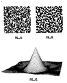
- Figs. 1A-C demonstrate pictorially the properties of the operation.
- the two-dimensional autocorrelation surface, R s ( ⁇ ) is measured empirically by filtering the random dot pattern shown in Fig. 1A with a ⁇ 2G operator which has a center diameter (w) that is 2.3 times the dot size.
- Fig. 1B shows the sign of the result.
- the autocorrelation of this binary pattern is then measured to produce the surface plotted in Fig. 1C.
- the independent axes of this perspective plot are horizontal and vertical disparity.
- R s ( ⁇ ) exhibits several valuable characteristics.
- the convolution sign is a binary representation
- the correlation peak is automatically normalized to 1 independent of image contrast. This means that peak height can be used as a direct measure of the noise present between the correlated image patches.
- the peak is pointed and has a near linear roll-off with distance down to zero correlation. This gives the two-dimensional correlation surface the shape of an inverted cone.
- the correlation peak is relatively wide at its base with a width of approximately the center diameter (w) of the ⁇ 2G operator, which aids sub-pixel interpolation of the peak position.
- the empirical measurement is a close fit to Equation 1 above.
- Another important factor in the CAD registration problem is the low signal to noise ratio caused by the difficulty of estimating edge contrasts and from other difficult to model effects such as specularities and interference fringes.
- some significant fraction of the imaged device must be treated as noise when aligning to the remainder.
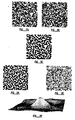
- Figs. 2A-F illustrate a situation where the signal to noise ratio is 1:1. This noise level is characteristic of some of the more difficult process steps encountered in photolithography and is a serious challenge to conventional alignment techniques.
- Fig. 2A is a random dot pattern and Fig. 2B is the same pattern with half of its dots replaced with another random pattern, which simulates a situation with noise equal to the signal level.
- Figs. 2C-D are the sign patterns obtained by convolving the patterns of Figs. 2A-B respectively with a ⁇ 2G operator with a center diameter (w) that is 2.3 times the dot size.
- Fig. 2E shows the locations where the patterns of Figs 2C-D differ.
- Fig. 2F plots the cross-correlation function obtained between the patterns of Figs 2C-D with a signal to noise ratio of 1:1. The noise brings the peak height down to half the height of the autocorrelation function shown in Fig. 1C, but it is still prominent and can be localized with subpixel resolution.
- Correlation values are measured at integral-pixel disparities, but these measurements can be treated as samples from a continuous underlying function.
- the location of the peak of the underlying function can be calculated to subpixel precision by fitting a symmetric peak model to the integral correlation data.
- the resolution obtained by this method depends on the precision to which the correlation values can be measured.
- an approximate upper bound on the measurement's standard deviation for square correlation windows is: ⁇ ⁇ w/(2d) where d is the window diameter and w is the center diameter of the ⁇ 2G operator.
- the correlation window is 10w in diameter, the correlation measurement will have a standard deviation on the order of 5 percent or less.
- a first application of the alignment technique of the invention is directed to positioning a movable element relative to a fixed workpiece.
- An example to be described below is locating the exact position where an IC should be placed on a PCB by aligning to the traces in the vicinity of the IC placement sites.
- a standard method for navigating an IC placement tool over a PCB is to position the PCB accurately using mechanical stops or alignment fiducial marks, and then to move either the PCB or the placement tool using precision mechanisms whose accuracy is relied upon to achieve the desired relative positions and orientations.
- precision mechanisms are more expensive, slower, and more prone to breakdown than low-accuracy mechanical drives. The problem is aggravated in the case of large boards.
- the present invention requires only that the drive mechanism have enough long range accuracy to get the tool and the PCB approximately registered, and that the drive mechanism be precisely controllable over small distances.
- Fig. 3 is a simplified side view of apparatus 10 for mounting an IC device 12 at one of a number of placement sites on a circuit board 15.
- a positioning head 17 is mounted for linear movement along an axis denoted by an arrow 20.
- the head carries a camera 22 and a placement actuator 25 which carries a device holder 27.
- the placement actuator and camera are oriented such that when the camera's optical axis intersects the nominal center of the placement site, actuator 25, when energized, places the IC with its center at that location.
- actuator 25 when energized, places the IC with its center at that location.
- various offsets are possible, as long as the relationship is known.
- the procedure for placing IC 12 on PCB 15 is as follows.
- the CAD database for the PCB contains coordinates for the IC placement site, and these are communicated to the positioning mechanism which drives the tool head to the right vicinity, given the possibly limited long-range accuracy of the positioning mechanism, and the possibility of errors in positioning the board on the apparatus.
- Camera 22 provides a video image centered at the nominal placement site. This is shown schematically in Fig. 4A where the initial positioning results in the desired IC placement site being displaced to the left and above the nominal placement site in the center of the image.
- the placement actuator were it to be energized, would put the IC in the wrong place (namely at the center of the image).
- the apparatus must move the positioning head so that the image is centered on the desired IC placement site, as shown schematically in Fig. 4B.
- the technique for determining the necessary additional displacement of the positioning head is carried out by correlating the camera image of Fig. 4A with a synthetic image from the CAD database.
- the resulting peak location is a numerical measure of the distance of the tool head from its desired location. Since this is a small increment, an instruction to move the tool head by that amount results in proper placement of the tool head. If the required displacement is larger than that which will guarantee placement to within tolerances, the procedure can be repeated and a new correlation, presumably with a much smaller displacement and required movement.
- Figs. 5A-B show a side-by-side comparison of the real grey-level camera image (on the left) and the binarized synthetic image of the matching region of the board (on the right).
- the synthetic CAD image was generated by the procedure described in Appendix 1. Note that the synthetic image was scaled, rather than the camera image being scaled. This is simpler in the sense that the need for bilinear resampling was avoided, but it is advantageous only because the database for a PCB is typically much smaller than that for an IC, and this allows relatively rapid generation of synthetic images.
- Figs. 6A and B show the results of the filtering and binarizing operation.
- a correlation program was used to determine the position at which the synthetic image best aligned with the real image, and interpolation technique described above was used to obtain the alignments to subpixel precision.
- the actual placement of the IC insertion points on the board were measured and the values compared to the nominal dimensions specified in the database, to generate an error value at each of the IC insertion points.
- the board was moved under the fixed camera by the use of a precision stepping x-y table, and a series of camera images were returned. By stepping the table in the nominal placement pattern of the IC locations, and correlating the real image at each location with the synthetic image from the database at the matching location, the difference between the nominal and measured locations of the IC insertion points was measured.
- Fig. 7 The results of this measurement are shown graphically in Fig. 7, as a map of the difference between the nominal and actual locations over a 6-inch by 6-inch area of the board.
- each IC location is marked with a box.
- the measured error difference between nominal and actual position of that section of the board traces
- the length and direction of the vector away from the box center indicates the magnitude and direction of the measured error
- the box provides a reference length of 1 pixel by 1 pixel, corresponding to approximately 0.005 inch in this case.
- the map shows that the errors are small (less than 0.7 pixel, or 0.0035 inch), as would be expected for a good-quality board.
- Figs. 8A-D and 9A-D show these errors plotted as graphs, with a best-fit linear approximation to the actual data points, for each row of IC insertion points as shown in the map of Fig. 7.
- a second application of the alignment technique of the invention is directed to the measurement of the relative alignment between parts of a completed (or partially completed) device that were placed in separate steps.
- One example is the alignment between two layers of metal tracks deposited on the surface of an integrated circuit.
- Another example is the alignment of a surface mount IC on a PCB. These will be described in order.
- Figs. 10A-B show examples of synthetic images representing the metal-1 and metal-2 layers of a region of a chip
- Fig. 11 shows the image of the same region of the physical chip observed using a video camera attached to a microscope.
- the synthetic CAD images were generated by the procedure described in Appendix 2.
- Image processing tools employing standard bilinear resampling techniques were used to scale the images acquired by the video camera through the microscope (at a known resolution) to the same scale as the synthetic CAD images.
- Convolution techniques were used to perform filtering on both the synthetic images and on the real image to obtain the sign bit of the Laplacian of the Gaussian of both the synthetic images and the real image, using the same scale of Gaussian.
- Figs. 12A-B show the sign of the filtered synthetic images
- Fig. 13 shows the sign of the filtered image of the physical device.
- FIGs. 14A-B show the correlation results for the metal-1 and metal-2 layers respectively.
- the metal-1 results show a clear peak, from which an accurate measurement in both dimensions may be made.
- the metal-2 results show a pronounced ridge, with a small peak. This is because there were very few features in the chip with vertical orientation in the metal-2 layer; so that there is very little for the correlation to key upon. However, the small peak, in spite of the noise, is still larger than any other noise peaks, and yields plausible results.
- the method described above for estimating peak position to sub-pixel accuracy was used to obtain the alignment result.
- the alignment figures are given below (dimensions are in pixels, which are 0.5 microns):
- Subtracting these values gives a relative alignment between the two layers of (0.08, 0.54) in pixels, or (0.04, 0.27) in microns, which is within tolerance for this chip.
- a second example is measuring the alignment of a surface mounted IC device relative to the PCB traces.
- This method includes the steps of: obtaining an optical image of the PCB including the part in question; generating a synthetic CAD image for the PCB in the vicinity of the part; filtering and binarizing the two images; determining the alignment between the processed CAD image for the PCB and the processed optical image; calculating from this alignment the exact location (in pixel coordinates) at which the IC device should be located based upon the positions of the PCB traces in the optical image; and determining the location of the IC device to ascertain whether the device is located in the proper position relative to the board traces.
- the latter step could entail applying a conventional method (perhaps based upon edge finding, or casting of shadows by the IC device in low-angle illumination). Although it is in theory possible to determine the position of the device based upon a synthetic image of the device, using filtering and correlation, the device is typically too small for the method to work reliably - a larger image area is needed for accurate alignment.
- This technique is based upon the assumption that features observed in the image of the physical object, which are not represented in the CAD data for the object, are uncorrelated, and can be treated as noise. However, in some cases this is not the case. For example, in the image of the chip, the second metal layer is visible, and the polysilicon layer is also partly visible. In the case of a circuit board, the main noise source is the texture of the board substrate; however, parts which have been placed upon the board, or holes drilled in the substrate, may introduce an additional correlated noise source.
- a further aspect of the invention contemplates making an additional synthetic noise-feature image (or mask) containing representations of the positions of these other features, and using this image to suppress or mask pixels near the noise features from participating in the correlation.
- a mask image might be obtained by completing a binary image showing the noise features (holes and part positions on a circuit board, or other layers on an IC) and dilating that image by convolving with a disc shaped operator of diameter equal to a few standard deviations of the expected misalignment of the noise features from their nominal positions.
- One way to build a model would be to model the way in which layers as described in the CAD database affect the surface height of the chip, in effect simulating the physical processes which were used to create the chip, in building a surface height map.
- Running a gradient operator over the surface map provides locations where high reflectivity might be expected, and the template is created from this data, as before, by performing the Laplacian and Gaussian filtering and taking the sign image.
- the hardware described below includes a ⁇ 2G convolver and a correlator that does five 1000-point correlations in parallel in 100 ⁇ s and allows the points correlated to be specified on a pixel by pixel basis.
- the hardware thus performs the massive computation at video rates, and can be implemented on just three standard multibus boards constructed with off-the-shelf parts no more complex than 4-bit adders.
- the following techniques are key to accomplishing this acceleration:
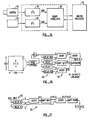
- Fig. 15 is a block diagram showing the basic hardware configuration.
- a video camera 100 and a CAD image generator 102 communicate their data streams to respective convolution circuits 105 and 107.
- the sign outputs are communicated to a binary correlator 110.
- a control processor 112 interfaced to the system over a low bandwidth link, controls correlator 110 and receives and interprets correlation measurements.
- the Laplacian of Gaussian filtering on the synthetic CAD image would be performed off-line, in software, and thus the second convolution circuit 107 would not be required.
- the experimental hardware is implemented using FAST TTL parts on wire-wrapped multibus boards.
- One board contains a Laplacian convolver; a second type of board contains a Gaussian convolver, of which there are several instances; a third board contains the correlators.
- the circuitry for performing the Laplacian operation is implemented as a 3-by-3 convolution as shown in Fig. 16.
- a video signal from camera 100 is digitized to produce a digital raster signal which is passed into a cascade of four delay modules 120. Two of these modules delay their inputs for a single pixel clock and the other two introduce delays one less than the number of pixels on a line from the camera.
- the combination obtains five parallel samples from a cross shaped region of the image. This pattern of samples moves over the image one pixel position to the right with each pixel clock and it wraps around at the end of the image in raster fashion.
- the five parallel samples, designated A through E, are supplied to an adder tree 125 configured to calculate the 3 by 3 discrete approximation to the Laplacian, 4C-(A+B+D+E).
- the resulting Laplacian raster signal is output to the Gaussian convolver which follows in the pipeline.
- Fig. 17 shows circuitry for computing a two-dimensional Gaussian convolution of the Laplacian raster signal.
- One pleasant property of multiple-dimensional Gaussian convolutions is that they can be decomposed into a cascade of one-dimensional Gaussian convolutions, thereby greatly reducing the size of the computation for large operators.
- the circuitry is implemented as a simple 3-point filter with binomial weights of 1/4, 1/2, 1/4.
- delay modules 130 are used to create three parallel samples from the raster input which are fed to an adder tree 135 with appropriate shifts to achieve the indicated scaling.
- the data values here are signed numbers so shifting bits to divide by 2 may require the addition of a carry bit to the prior addition to prevent round off bias.
- Delay elements 130 are variable delay modules allowing delays from 1 pixel to several times the line length of the image. Setting the delays to 1 pixel each creates a 3-point horizontal filter. Setting the delay to the line length creates a 3-point vertical filter. Other choices for the delays are also useful and will be discussed in a later section.
- Fig. 18 shows the circuitry for computing a 7-point Gaussian.
- Application of a cascade of three G3 filters in series all using the same delay creates the effect of convolution with a 7-point binomial distribution, ("G7 filter").
- G7 filter This size produces a fairly close approximation to a one-dimensional Gaussian.
- a G7 filter reduces the amplitude of a Laplacian signal by about a factor of 2 so one bit of down shifting is eliminated at the end of the last G3 element in the G7 module. This keeps the numbers fairly well normalized in the pipeline. 16-bit integer arithmetic is sufficient; 12-bit arithmetic at a minimum is required.
- Two such 7-point Gaussian filters 140 and 145 with one set up as a horizontal Gaussian and the other as a vertical Gaussian yield a two-dimensional 7-by-7 Gaussian filter, G 7x7 , when the delay parameter N is set to 1.
- G 7x7 many applications require Gaussian filters much larger than the 7-by-7 Gaussian filter, G 7x7 , described above.
- a bigger filter can be constructed by cascading additional G 7x7 modules together. However, this is not cost effective with the simple G 7x7 modules since for each factor of 2 increase in filter diameter, the hardware would have to be quadrupled in size.
- a more efficient approach makes use of the fact that the first G 7x7 convolution low-pass filters the input sufficiently to allow sampling only every other pixel with no appreciable aliasing.
- every other element of a subsequent 14-by-14 Gaussian filter can be set to zero with no significant loss.
- a 14-by-14 Gaussian filter with alternate elements set to zero is obtained from the G 7x7 module with its delay parameter, N set to 2.
- Fig. 19 shows a ⁇ 2G filter incorporating two G 7x7 modules 150 and 152 in this manner. Further G 7x7 modules can be added with N set to increasing powers of 2 to achieve further doublings of
- the G 7x7 hardware module described above was implemented on a single standard multibus board using 16-bit precision in all computations. FAST TTL logic parts allow conservative operation at a 10 MHz pixel rate.
- Fig. 20 shows a hardware correlator 160 that allows configurable correlation windows. Correlation of ⁇ 2G sign arrays can be efficiently implemented in hardware using high speed static RAMs as image buffers - a single 64K-by-1 chip buffers a 256-by-256 array of ⁇ 2G sign bits. Additional static RAMs can be used as tables specifying a large set of pairs of x,y coordinates which together define a correlation window.
- a common index generator shown as a counter, addresses the A and B correlation window tables which store (x,y) pairs of window offsets. These two tables store identical offsets when translation disparities are to be measured between the two image regions correlated.
- the table memories can be made large enough to hold many window definitions at a time and the window number register is used to select the desired window for a particular correlation.
- Each table outputs x and y offset values which are added to a base position to set the overall position of the window on the image.
- the values in these registers are also adjusted to cancel any translation disparities that exist between the A and B images at the window position.
- the resulting x and y positions together form an address which is sent to the image memory buffers.
- the image buffers output pixel values which are correlated and the result is added into an accumulator.
- the image memories are loaded with the sign bit of Laplacian of Gaussian filtered intensity images and the correlator is an XOR gate.
- the hardware correlator as implemented, is fairly simple and uses standard TTL FAST parts on a wire-wrapped multibus board.
- the design follows Fig. 19, except that there are five instances of the "B" side of the correlator running in parallel. This allows five correlations to be carried out in parallel against a single window defined by the "A" side of the correlator.
- the image memories are 64K-by-1 static rams and are dual ported (stores of sign bits from the ⁇ 2G convolver are interleaved with accesses by the correlator).
- the hardware runs at a 10 MHz pixel rate which means that five 1000-point correlations are done in 100 ⁇ s plus the multibus overhead for starting the correlator and reading back results.
- the present invention provides a simple technique for correlating CAD images with images of the devices made from them.
- the technique is largely immune to noise and requires few adjustments.
- An SEM can be used to form an image of an IC.
- the conductors at high voltage reflect electrons brightly, while conductors at low voltage and the IC substrate are effectively invisible.
- the synthetic image contains all the conductors that might be visible, and treats the absence of those conductors that are not at a high voltage in the observed image as noise.
- An alignment is obtained between the image and the database. If two different images are obtained, one from a known good circuit, and one from a circuit which is malfunctioning, and are to be compared, they can both be registered to the database, which will reveal their alignment relative to each other. A simple substraction of one image from the other, at the appropriate alignment, will then reveal the contrast between the conductors which are not the same in the images of the good and malfunctioning circuits.
- the SEM can be instructed to probe a single spot of the integrated circuit rather than scan the entire region of the image, to obtain a time varying trace of the signal at that point.
- An operator might indicate the connection to be probed on a schematic diagram of the circuit; this is linked to the data describing the physical connections in the database, and hence can be turned into coordinates in model space, but in order to relate this to beam position on the microscope, a registration between the observed image of the circuit and the database is required.
- the system could build a synthetic image of part of the circuit near the point to be probed, and perform a registration (using the method described above) on the scanned image to identify the exact position to be probed in acquisition mode.
- the filtering of the images was described above in terms of Laplacian and Gaussian convolution operations, other high pass and low pass filtering techniques can be used. Indeed the preferred hardware uses a 3-by-3-point discrete approximation to the Laplacian and a binomial approximation to the Gaussian. Alternatively, the Laplacian of Gaussian can be approximated by a difference of Gaussians.
- a design file for PCB trace geometry may conform to a variety of standards: in the case described above, the file was in Gerber format, in which the geometry is specified as motions of an exposure head relative to a recording film.
- the exposure head creates an image of a selectable aperture, and this image is moved over the recording film to selectively expose regions of the film in the desired geometry.
- the apertures are typically circular or square, to create lines and their terminations, but may be more complex, to create special shapes such as logos or alignment fiducial marks.
- the apertures can be physically changed in the exposure head, to allow the efficient creation of the geometry required by a specific job, it is necessary to use both the main database and the aperture selection table which would be used with that database, to create a synthetic image mimicking the actual board geometry.
- the software was written to read the Gerber database file and the aperture selection table, and to create synthetic images as binary two-dimensional pixel arrays.
- the software provided for setting image scale factors independently on the orthogonal axes, and for offsets on these axes, so that the synthetic images could be scaled and placed to match the real board images from the camera. It is important to note that the synthetic images were binary, i.e. consisted of black or white values only. This allows the software for generating the synthetic images to be simple and fast compared to that which would be needed to create grey-level images by modeling the effects of illumination, board color, and camera spectral response.
- the particular CAD database used in this example consists of a file containing a list of geometrical features such as rectangles and polygons, with sizes and positions of such features on different layers of the chip.
- the CAD database is expressed in hierarchical form: a set of features which make up a 'cell' is described once, and then that cell may be invoked within another larger cell definition. The complete chip may then be considered as simply the root cell in the hierarchy of cell definitions.
- Each cell has its own coordinate system as it is being defined.
- a set of mathematical transforms affine transforms
- Such a set of transforms may be specified in the form of a homogeneous matrix, which multiplies the coordinates of the untransformed features to yield the coordinates in transformed space.
- another set of transformations is applied.
- the placement of basic geometry in the root cell definition is subject to a set of transforms which may be expressed as the product of each of the matrices for the individual cells.
- a software program normally used for generating raster pictures of the CAD data for the chip on a color plotter was modified to generate a raster image to be used as a template for the matching process.
- This program reads in the CAD data, forming a representation of the cell definitions and transforms required to map each cell into the coordinate system of its parent cell.
- a description of the appearance of each layer in terms of its color in the output image is also read in.
- a raster image array is allocated and cleared to a background value, and the geometry specified by the root cell is drawn into the array, item by item.
- An initial transform matrix maps the coordinates of the root cell into the coordinates of the image array. If an image of only part of the entire database is desired, this may be expressed in the scaling and transformations of this transform matrix.
- the current transformation matrix is copied, multiplied by the transformation matrix for the cell being invoked, and pushed onto the stack, becoming the current transform.
- basic geometry is invoked, it is transformed according to the current transform, which expresses all the transforms to map the geometry through all its parent cells to the coordinate system of the root cell and finally to the coordinate system of the image array. If the geometry falls inside the area of the image array, then pixels falling within the area described by the geometry are colored according to the description of the appearance of the layer of the geometry.
Landscapes
- Engineering & Computer Science (AREA)
- Physics & Mathematics (AREA)
- General Physics & Mathematics (AREA)
- Theoretical Computer Science (AREA)
- Computer Vision & Pattern Recognition (AREA)
- Multimedia (AREA)
- Image Processing (AREA)
- Image Analysis (AREA)
- Closed-Circuit Television Systems (AREA)
Applications Claiming Priority (2)
| Application Number | Priority Date | Filing Date | Title |
|---|---|---|---|
| US30494389A | 1989-01-31 | 1989-01-31 | |
| US304943 | 1989-01-31 |
Publications (2)
| Publication Number | Publication Date |
|---|---|
| EP0381067A2 true EP0381067A2 (fr) | 1990-08-08 |
| EP0381067A3 EP0381067A3 (fr) | 1992-08-12 |
Family
ID=23178632
Family Applications (1)
| Application Number | Title | Priority Date | Filing Date |
|---|---|---|---|
| EP19900101560 Withdrawn EP0381067A3 (fr) | 1989-01-31 | 1990-01-26 | Méthode d'enregistrement de modèle C.A.D. sur des images vidéo avec addition de fouillis |
Country Status (2)
| Country | Link |
|---|---|
| EP (1) | EP0381067A3 (fr) |
| JP (1) | JPH03148774A (fr) |
Cited By (10)
| Publication number | Priority date | Publication date | Assignee | Title |
|---|---|---|---|---|
| FR2693813A1 (fr) * | 1992-07-20 | 1994-01-21 | Commissariat Energie Atomique | Procédé de réalisation d'une image de référence synthétisée à partir de données contenues dans une base de données CAO. |
| FR2697930A1 (fr) * | 1992-11-09 | 1994-05-13 | Commissariat Energie Atomique | Procédé de réalisation d'une image de référence synthétisée pour l'inspection d'objets. |
| EP0619551A3 (fr) * | 1993-03-15 | 1995-08-16 | Schlumberger Technologies Inc | Détermination du décalage entre images d'un circuit intégré. |
| WO2000007146A1 (fr) * | 1998-07-28 | 2000-02-10 | General Electric Company | Procede et appareil pour calibrer un capteur d'images sans contact |
| US6411915B1 (en) | 1998-07-28 | 2002-06-25 | General Electric Company | Method and apparatus for calibrating a non-contact range sensor |
| US6748112B1 (en) | 1998-07-28 | 2004-06-08 | General Electric Company | Method and apparatus for finding shape deformations in objects having smooth surfaces |
| US6985238B2 (en) | 2002-09-25 | 2006-01-10 | General Electric Company | Non-contact measurement system for large airfoils |
| US7327857B2 (en) | 2004-03-09 | 2008-02-05 | General Electric Company | Non-contact measurement method and apparatus |
| US7543326B2 (en) | 2002-06-10 | 2009-06-02 | Microsoft Corporation | Dynamic rate control |
| US7567619B2 (en) | 2002-06-24 | 2009-07-28 | Microsoft Corporation | Video deblocking |
Families Citing this family (1)
| Publication number | Priority date | Publication date | Assignee | Title |
|---|---|---|---|---|
| US5600734A (en) * | 1991-10-04 | 1997-02-04 | Fujitsu Limited | Electron beam tester |
Family Cites Families (1)
| Publication number | Priority date | Publication date | Assignee | Title |
|---|---|---|---|---|
| EP0254644A3 (fr) * | 1986-07-22 | 1990-07-18 | Schlumberger Technologies, Inc. | Alignement de masque et mesure de dimensions critiques sur des circuits intégrés |
-
1990
- 1990-01-26 EP EP19900101560 patent/EP0381067A3/fr not_active Withdrawn
- 1990-01-31 JP JP2019359A patent/JPH03148774A/ja active Pending
Cited By (16)
| Publication number | Priority date | Publication date | Assignee | Title |
|---|---|---|---|---|
| FR2693813A1 (fr) * | 1992-07-20 | 1994-01-21 | Commissariat Energie Atomique | Procédé de réalisation d'une image de référence synthétisée à partir de données contenues dans une base de données CAO. |
| EP0580481A1 (fr) * | 1992-07-20 | 1994-01-26 | Commissariat A L'energie Atomique | Procédé de réalisation d'une image de référence synthétisée à partir de données contenues dans une base de données CAO |
| FR2697930A1 (fr) * | 1992-11-09 | 1994-05-13 | Commissariat Energie Atomique | Procédé de réalisation d'une image de référence synthétisée pour l'inspection d'objets. |
| EP0597762A1 (fr) * | 1992-11-09 | 1994-05-18 | Commissariat A L'energie Atomique | Procédé de réalisation d'une image de référence synthétisée pour l'inspection d'objets |
| US5452369A (en) * | 1992-11-09 | 1995-09-19 | Commissariat A L'energie Atomique | Process for producing a synthesized reference image for the inspection of objects |
| EP0619551A3 (fr) * | 1993-03-15 | 1995-08-16 | Schlumberger Technologies Inc | Détermination du décalage entre images d'un circuit intégré. |
| US5604819A (en) * | 1993-03-15 | 1997-02-18 | Schlumberger Technologies Inc. | Determining offset between images of an IC |
| US6411915B1 (en) | 1998-07-28 | 2002-06-25 | General Electric Company | Method and apparatus for calibrating a non-contact range sensor |
| WO2000007146A1 (fr) * | 1998-07-28 | 2000-02-10 | General Electric Company | Procede et appareil pour calibrer un capteur d'images sans contact |
| US6748112B1 (en) | 1998-07-28 | 2004-06-08 | General Electric Company | Method and apparatus for finding shape deformations in objects having smooth surfaces |
| US7543326B2 (en) | 2002-06-10 | 2009-06-02 | Microsoft Corporation | Dynamic rate control |
| US7567619B2 (en) | 2002-06-24 | 2009-07-28 | Microsoft Corporation | Video deblocking |
| US7567618B2 (en) | 2002-06-24 | 2009-07-28 | Microsoft Corporation | Video deblocking |
| US7660351B2 (en) * | 2002-06-24 | 2010-02-09 | Microsoft Corporation | Video deblocking |
| US6985238B2 (en) | 2002-09-25 | 2006-01-10 | General Electric Company | Non-contact measurement system for large airfoils |
| US7327857B2 (en) | 2004-03-09 | 2008-02-05 | General Electric Company | Non-contact measurement method and apparatus |
Also Published As
| Publication number | Publication date |
|---|---|
| JPH03148774A (ja) | 1991-06-25 |
| EP0381067A3 (fr) | 1992-08-12 |
Similar Documents
| Publication | Publication Date | Title |
|---|---|---|
| US6639685B1 (en) | Image processing method using phase-shifted fringe patterns and curve fitting | |
| US6363168B1 (en) | Measurement position determination on a semiconductor wafer | |
| Garcia et al. | A combined temporal tracking and stereo-correlation technique for accurate measurement of 3D displacements: application to sheet metal forming | |
| US8050461B2 (en) | Depth-varying light fields for three dimensional sensing | |
| US7382471B2 (en) | Non-contact apparatus and method for measuring surface profile | |
| US5559334A (en) | Epipolar reconstruction of 3D structures | |
| JP4901903B2 (ja) | 三次元検査システム | |
| US10706570B2 (en) | System and method to acquire the three-dimensional shape of an object using a moving patterned substrate | |
| US5119444A (en) | System for expedited computation of laplacian and gaussian filters and correlation of their outputs for image processing | |
| Ghalib et al. | Soil particle size distribution by mosaic imaging and watershed analysis | |
| EP0381067A2 (fr) | Méthode d'enregistrement de modèle C.A.D. sur des images vidéo avec addition de fouillis | |
| JP2001519945A (ja) | 三次元画像化方法及びその装置 | |
| US6681039B1 (en) | Fiducial mark search using sub-models | |
| EP0769674A2 (fr) | Analyse des franges électroniques pour la détermination de contours de surfaces | |
| EP0356727A2 (fr) | Mesure de position de cible basée sur la symétrie | |
| Deng et al. | An INSPECT measurement system for moving objects | |
| Negahdaripour et al. | Recovering shape and motion from undersea images | |
| Griffin et al. | Process capability of automated visual inspection systems | |
| Mileski et al. | Development of a computer vision-based system for part referencing in CNC machining centers | |
| Zhenzhong et al. | The application of machine vision in inspecting position-control accuracy of motor control systems | |
| Lynch et al. | Backpropagation neural network for stereoscopic vision calibration | |
| Cardenas-Garcia et al. | Projection moiré as a tool for the automated determination of surface topography | |
| Chen et al. | Self recalibration of a structured light vision system from a single view | |
| CN111612071A (zh) | 一种从曲面零件阴影图生成深度图的深度学习方法 | |
| Bae et al. | A hybrid scheme incorporating stereo-matching and shape-from-shading for spatial object recognition |
Legal Events
| Date | Code | Title | Description |
|---|---|---|---|
| PUAI | Public reference made under article 153(3) epc to a published international application that has entered the european phase |
Free format text: ORIGINAL CODE: 0009012 |
|
| AK | Designated contracting states |
Kind code of ref document: A2 Designated state(s): DE FR GB IT NL |
|
| PUAL | Search report despatched |
Free format text: ORIGINAL CODE: 0009013 |
|
| AK | Designated contracting states |
Kind code of ref document: A3 Designated state(s): DE FR GB IT NL |
|
| 17P | Request for examination filed |
Effective date: 19921217 |
|
| 17Q | First examination report despatched |
Effective date: 19950206 |
|
| STAA | Information on the status of an ep patent application or granted ep patent |
Free format text: STATUS: THE APPLICATION IS DEEMED TO BE WITHDRAWN |
|
| 18D | Application deemed to be withdrawn |
Effective date: 19950801 |