EP0382046A2 - Composition de réserve électroconductrice, procédé de formation et utilisation - Google Patents
Composition de réserve électroconductrice, procédé de formation et utilisation Download PDFInfo
- Publication number
- EP0382046A2 EP0382046A2 EP90101765A EP90101765A EP0382046A2 EP 0382046 A2 EP0382046 A2 EP 0382046A2 EP 90101765 A EP90101765 A EP 90101765A EP 90101765 A EP90101765 A EP 90101765A EP 0382046 A2 EP0382046 A2 EP 0382046A2
- Authority
- EP
- European Patent Office
- Prior art keywords
- resist composition
- electrically conductive
- polymer
- resist
- composition according
- Prior art date
- Legal status (The legal status is an assumption and is not a legal conclusion. Google has not performed a legal analysis and makes no representation as to the accuracy of the status listed.)
- Withdrawn
Links
Images
Classifications
-
- C—CHEMISTRY; METALLURGY
- C09—DYES; PAINTS; POLISHES; NATURAL RESINS; ADHESIVES; COMPOSITIONS NOT OTHERWISE PROVIDED FOR; APPLICATIONS OF MATERIALS NOT OTHERWISE PROVIDED FOR
- C09D—COATING COMPOSITIONS, e.g. PAINTS, VARNISHES OR LACQUERS; FILLING PASTES; CHEMICAL PAINT OR INK REMOVERS; INKS; CORRECTING FLUIDS; WOODSTAINS; PASTES OR SOLIDS FOR COLOURING OR PRINTING; USE OF MATERIALS THEREFOR
- C09D5/00—Coating compositions, e.g. paints, varnishes or lacquers, characterised by their physical nature or the effects produced; Filling pastes
- C09D5/24—Electrically-conducting paints
-
- G—PHYSICS
- G03—PHOTOGRAPHY; CINEMATOGRAPHY; ANALOGOUS TECHNIQUES USING WAVES OTHER THAN OPTICAL WAVES; ELECTROGRAPHY; HOLOGRAPHY
- G03F—PHOTOMECHANICAL PRODUCTION OF TEXTURED OR PATTERNED SURFACES, e.g. FOR PRINTING, FOR PROCESSING OF SEMICONDUCTOR DEVICES; MATERIALS THEREFOR; ORIGINALS THEREFOR; APPARATUS SPECIALLY ADAPTED THEREFOR
- G03F7/00—Photomechanical, e.g. photolithographic, production of textured or patterned surfaces, e.g. printing surfaces; Materials therefor, e.g. comprising photoresists; Apparatus specially adapted therefor
- G03F7/004—Photosensitive materials
- G03F7/027—Non-macromolecular photopolymerisable compounds having carbon-to-carbon double bonds, e.g. ethylenic compounds
-
- C—CHEMISTRY; METALLURGY
- C09—DYES; PAINTS; POLISHES; NATURAL RESINS; ADHESIVES; COMPOSITIONS NOT OTHERWISE PROVIDED FOR; APPLICATIONS OF MATERIALS NOT OTHERWISE PROVIDED FOR
- C09D—COATING COMPOSITIONS, e.g. PAINTS, VARNISHES OR LACQUERS; FILLING PASTES; CHEMICAL PAINT OR INK REMOVERS; INKS; CORRECTING FLUIDS; WOODSTAINS; PASTES OR SOLIDS FOR COLOURING OR PRINTING; USE OF MATERIALS THEREFOR
- C09D5/00—Coating compositions, e.g. paints, varnishes or lacquers, characterised by their physical nature or the effects produced; Filling pastes
- C09D5/08—Anti-corrosive paints
-
- C—CHEMISTRY; METALLURGY
- C09—DYES; PAINTS; POLISHES; NATURAL RESINS; ADHESIVES; COMPOSITIONS NOT OTHERWISE PROVIDED FOR; APPLICATIONS OF MATERIALS NOT OTHERWISE PROVIDED FOR
- C09D—COATING COMPOSITIONS, e.g. PAINTS, VARNISHES OR LACQUERS; FILLING PASTES; CHEMICAL PAINT OR INK REMOVERS; INKS; CORRECTING FLUIDS; WOODSTAINS; PASTES OR SOLIDS FOR COLOURING OR PRINTING; USE OF MATERIALS THEREFOR
- C09D7/00—Features of coating compositions, not provided for in group C09D5/00; Processes for incorporating ingredients in coating compositions
- C09D7/40—Additives
-
- G—PHYSICS
- G03—PHOTOGRAPHY; CINEMATOGRAPHY; ANALOGOUS TECHNIQUES USING WAVES OTHER THAN OPTICAL WAVES; ELECTROGRAPHY; HOLOGRAPHY
- G03F—PHOTOMECHANICAL PRODUCTION OF TEXTURED OR PATTERNED SURFACES, e.g. FOR PRINTING, FOR PROCESSING OF SEMICONDUCTOR DEVICES; MATERIALS THEREFOR; ORIGINALS THEREFOR; APPARATUS SPECIALLY ADAPTED THEREFOR
- G03F7/00—Photomechanical, e.g. photolithographic, production of textured or patterned surfaces, e.g. printing surfaces; Materials therefor, e.g. comprising photoresists; Apparatus specially adapted therefor
- G03F7/004—Photosensitive materials
- G03F7/027—Non-macromolecular photopolymerisable compounds having carbon-to-carbon double bonds, e.g. ethylenic compounds
- G03F7/032—Non-macromolecular photopolymerisable compounds having carbon-to-carbon double bonds, e.g. ethylenic compounds with binders
-
- H—ELECTRICITY
- H01—ELECTRIC ELEMENTS
- H01B—CABLES; CONDUCTORS; INSULATORS; SELECTION OF MATERIALS FOR THEIR CONDUCTIVE, INSULATING OR DIELECTRIC PROPERTIES
- H01B1/00—Conductors or conductive bodies characterised by the conductive materials; Selection of materials as conductors
- H01B1/06—Conductors or conductive bodies characterised by the conductive materials; Selection of materials as conductors mainly consisting of other non-metallic substances
- H01B1/12—Conductors or conductive bodies characterised by the conductive materials; Selection of materials as conductors mainly consisting of other non-metallic substances organic substances
- H01B1/124—Intrinsically conductive polymers
- H01B1/127—Intrinsically conductive polymers comprising five-membered aromatic rings in the main chain, e.g. polypyrroles, polythiophenes
Definitions
- the invention relates to an electrically conductive resist composition which can prevent electrostatic charges and the fields resulting therefrom, a method for their production and their use, in particular for the production of electron beam resists.
- the following can be used, for example: indium oxide, tin oxide or ITO layers on glass substrates, to which the resist is then applied (cf. Chem. Abstr. 102 , 229.567n).
- a resist composition which contains a conductive polymeric tetracyanoquinone dimethane (TCNQ) salt complex in a PMMA matrix in order to avoid the charging effects.
- TCNQ conductive polymeric tetracyanoquinone dimethane
- a disadvantage of this process is that TCNQ complexes are generally insoluble or poorly soluble, so that phase separation can occur when the resist is applied.
- TCNQ complexes are difficult to handle because of their toxicity and decompose even at elevated temperatures (cf. Chem. Abstr. 108 , 29440c).
- the object was therefore to provide electrically conductive resist compositions which do not have the disadvantages mentioned above and which, moreover, can be processed using the customary methods used in microelectronics.
- the invention thus relates to an electrically conductive resist, consisting essentially of at least one polymer sensitive to ionizing radiation and a soluble, electrically conductive oligomer or a soluble, electrically conductive polymer.
- the invention further relates to a method for producing an electrically conductive resist composition, characterized in that an electrically conductive oligomer or polymer dissolved in a suitable solvent is added to at least one polymer sensitive to ionizing radiation.
- conductive oligomers or conductive polymers Compounds whose solubility is sufficiently high in the solvents used in the resist formulations can in principle be used as conductive oligomers or conductive polymers. These include oligo- and polythiophene derivatives, which also have substituents in the 3-position. 3-Alkoxy-substituted oligo- and polythiophenes are preferably used.
- Examples are 3-butylthiophene, 3-pentylthiophene, 3-hexylthiophene, 3-octylthiophene, 3-dodecylthiophene, 3- (methoxyethoxyethoxymethyl) thiophene, 3,4-diethylthiophene, 3-butyl-4-methylthiophene, 3-methoxythiophene, 3- Ethoxythiophene, 3-propoxythiophene, 3- (methoxyethoxy) thiophene, 3-methoxy-4-methylthiophene, 3-ethyl-4-methoxythiophene, 3-butyl-4-methoxythiophene, 3-ethoxy-4-methylthiophene, 3-ethoxy-4 -ethylthiophene, 3-butoxy-4-methylthiophene, 3,4-dimethoxythiophene, 3-ethoxy-4-methoxythiophene or 3-butoxy-4-methylthiophene
- the alkoxy group comprises at least 6 carbon atoms, preferably 6 to 25 carbon atoms, as in 3-hexyloxythiophene, 3-heptyloxythiophene, 3-octyloxythiophene, 3- Nonyloxythiophene, 3-decyl oxythiophene, 3-undecyloxythiophene, 3-dodecyloxythiophene, 3-tetradecyloxythiophene, 3-pentadecyloxythiophene, 3-hexadecyloxythiophene, 3-octadecyloxythiophene, 3-eicosyloxythiophene, 3-docosyloxythiophene, 3- (3'-ethoxy), 3- (3'-2'-ethoxy) 4 ′, 4′-trimethylpentyloxy) thiophene, 3,4-dihexyloxythiophene,
- the addition of 0.01 to 10% by weight of the conductive oligomer or polymer to the dry substance of the formulation proves to be favorable, the preferred concentrations being between 0 , 1 and 5 wt .-%, in particular between 0.1 and 3 wt .-%.
- the solvents used are those which dissolve both the components of the formulation and the conductive oligomer or conductive polymer.
- Glycol ethers for example glycol monomethyl ether, glycol dimethyl ether, glycol monoethyl ether or propylene glycol monoalkyl ether, preferably propylene glycol methyl ether, aliphatic esters, for example ethyl acetate, hydroxyethyl acetate, alkoxyethyl, can be used acetate, n-butyl acetate, propylene glycol monoalkyl ether acetate, preferably propylene glycol methyl ether acetate or amyl acetate, ethers, for example dioxane or tetrahydrofuran, ketones, for example methyl ethyl ketone, methyl isobutyl ketone, cyclopentanone and cyclohexanone, dimethylformamide, dimethylacetamide, hexa
- the use of the conductive resist composition according to the invention is not restricted to insulating substrates.
- the particular advantage only comes into play when applied to highly insulating substrates.
- the following can be used as such: undoped semiconductor substrates, such as Si, Ge or GaAs with a small surface or volume conductivity, substrates with highly insulating coatings of organic or inorganic type, such as oxide layers, quartz, lithium niobate, strontium titanate, sapphire, diamond, but also insulating films made of organic Polymers, such as polyethylene terephthalate or films made of inorganic materials, such as membranes made of silicon, silicon carbide or beryllium.
- an adhesion promoter can be added to the resist.
- An adhesion promoter can also be applied to the substrate before coating.
- dyes, pigments, plasticizers, wetting agents and leveling agents for example polyglycols, cellulose ethers, preferably ethyl cellulose, can optionally be added to the radiation-sensitive mixtures according to the invention in order to improve special requirements such as flexibility, adhesion and gloss.
- the resist composition according to the invention can be prepared by first dissolving the electrically conductive oligomer or electrically conductive polymer in a suitable solvent and then adding it to a finished resist formulation or applying it separately.
- the conductive connection can also be dissolved together with the individual components of the resist formulation in a suitable solvent or solvent mixture. This takes place at a temperature between the melting point and the boiling point of the solvent or solvent mixture used, preferably in the range from 0 ° C. and 80 ° C., in particular from 20 ° C. and 60 ° C., optionally with stirring or other mixing techniques.
- the concentration of the main components in the solution is 0.1 to 30, preferably 0.5 to 10% by weight.
- the resist composition can be processed by the usual methods, such as spin coating or spray coating.
- the layer thickness can be adjusted within wide limits as required.
- drying takes place e.g. in an oven, on a hot plate or, in the case of web processing, in the drying tunnel at elevated temperature, preferably between 80 ° and 130 ° C.
- elevated temperature preferably between 80 ° and 130 ° C.
- a pre-drying step at room temperature can be used before drying at elevated temperature.
- the irradiation takes place with ionizing radiation, for example with electron radiation or X-rays, preferably with electron radiation.
- developers customary for the respective resist formulations are predominantly developers, which consist essentially of organic solvents.
- developers which consist essentially of organic solvents.
- aqueous or aqueous-alkaline developers can also be used.
- etch resistance is made possible in the following process steps by the developed resist layers for some time, e.g. B. 5 to 40 Minutes, at elevated temperature, possibly with simultaneous exposure to UV light.
- the resist composition according to the invention is used in the production of electron beam resists to prevent electrostatic charges and the fields resulting therefrom.
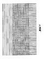
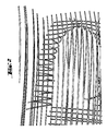
- Comparative Example A was repeated with the proviso that an insulating substrate (quartz) was used instead of the conductive substrate. With the same procedure, however, it was not possible to transfer the predetermined pattern (analogous to FIG. 1) into the resist. The structures shown in FIG. 2 were observed due to charging effects.
- an insulating substrate quartz
- Example 1 The resist composition from Example 1 was applied to an insulating quartz substrate in accordance with Comparative Example B. After irradiation and development as in Comparative Example A, good structure transfer without distortions as shown in FIG. 1 was obtained.
- Example 2 was repeated with the proviso that the proportion of the polydodecyloxythiophene was increased to 5% by weight of the solid substance.
- the specific conductivity obtained was 4.3 ⁇ 10 ⁇ 7 S / cm. The result corresponded to Fig. 2.
- the cathode consisted of stainless steel sheets 80 mm long and 55 mm wide.
- a carbon felt (basis weight approx. 0.3 kg / m2, specific surface (BET) approx. 1.5 m2 / g), 80 mm long, 55 mm wide and 3 mm thick was used as anode (geometric on both sides Area approx. 90 cm2).
- the anode was attached parallel to the cathode at a distance of 2 cm and separated using a polypropylene mesh spacer.
- the crude product was crushed mechanically, washed with water, dried, digested with methylene chloride for 12 h, then filtered off and dried.
- the material obtained was redissolved in acetonitrile and centrifuged at 10,000 rpm for 0.5 h and the centrifugate was evaporated to dryness in a rotary evaporator. 1.92 g of a solid with a bronze metal gloss were obtained.
- the elemental analysis gave the following values: 44.5% C, 3.2% H, 22.1% S, 9.4% F.
- a powder compact of the ground product had a specific conductivity of 1.8 ⁇ 10 -3 S / cm .
- a weight loss of less than 10% was observed with the DTG up to 245 ° C.
- the DSC showed a maximum at 325 ° C.
- the undoped form GPC showed that more than 80% of the product consisted of pentamers and hexamers.
Landscapes
- Physics & Mathematics (AREA)
- Chemical & Material Sciences (AREA)
- Spectroscopy & Molecular Physics (AREA)
- General Physics & Mathematics (AREA)
- Materials Engineering (AREA)
- Engineering & Computer Science (AREA)
- Life Sciences & Earth Sciences (AREA)
- Wood Science & Technology (AREA)
- Organic Chemistry (AREA)
- Electron Beam Exposure (AREA)
- Polyoxymethylene Polymers And Polymers With Carbon-To-Carbon Bonds (AREA)
- Exposure And Positioning Against Photoresist Photosensitive Materials (AREA)
- Addition Polymer Or Copolymer, Post-Treatments, Or Chemical Modifications (AREA)
- Materials For Photolithography (AREA)
- Compositions Of Macromolecular Compounds (AREA)
Applications Claiming Priority (2)
| Application Number | Priority Date | Filing Date | Title |
|---|---|---|---|
| DE3903421 | 1989-02-06 | ||
| DE3903421A DE3903421A1 (de) | 1989-02-06 | 1989-02-06 | Elektrisch leitfaehige resistmasse, verfahren zu ihrer herstellung und ihre verwendung |
Publications (2)
| Publication Number | Publication Date |
|---|---|
| EP0382046A2 true EP0382046A2 (fr) | 1990-08-16 |
| EP0382046A3 EP0382046A3 (fr) | 1991-10-23 |
Family
ID=6373485
Family Applications (1)
| Application Number | Title | Priority Date | Filing Date |
|---|---|---|---|
| EP19900101765 Withdrawn EP0382046A3 (fr) | 1989-02-06 | 1990-01-30 | Composition de réserve électroconductrice, procédé de formation et utilisation |
Country Status (10)
| Country | Link |
|---|---|
| US (1) | US5137799A (fr) |
| EP (1) | EP0382046A3 (fr) |
| JP (1) | JPH02245755A (fr) |
| KR (1) | KR900013033A (fr) |
| AU (1) | AU630414B2 (fr) |
| BR (1) | BR9000492A (fr) |
| CA (1) | CA2009167A1 (fr) |
| DE (1) | DE3903421A1 (fr) |
| FI (1) | FI900537A7 (fr) |
| ZA (1) | ZA90795B (fr) |
Cited By (1)
| Publication number | Priority date | Publication date | Assignee | Title |
|---|---|---|---|---|
| WO2002006898A3 (fr) * | 2000-06-26 | 2002-05-02 | Agfa Gevaert | Materiau et procede permettant de fabriquer un motif conducteur |
Families Citing this family (20)
| Publication number | Priority date | Publication date | Assignee | Title |
|---|---|---|---|---|
| JPH03137649A (ja) * | 1989-10-24 | 1991-06-12 | Matsushita Electric Ind Co Ltd | 微細パターン形成材料およびパターン形成方法 |
| JPH05226238A (ja) * | 1991-10-31 | 1993-09-03 | Internatl Business Mach Corp <Ibm> | E−ビームレジスト用の塩基現像可能な放電トップ層 |
| US7166241B1 (en) | 1993-03-03 | 2007-01-23 | International Business Machines Corporation | Water-soluble electrically conducting polymers, their synthesis and use |
| US5556706A (en) * | 1993-10-06 | 1996-09-17 | Matsushita Electric Industrial Co., Ltd. | Conductive layered product and method of manufacturing the same |
| US6022669A (en) * | 1995-05-02 | 2000-02-08 | Symetrix Corporation | Method of fabricating an integrated circuit using self-patterned thin films |
| DE19524132A1 (de) * | 1995-07-03 | 1997-01-09 | Bayer Ag | Kratzfeste leitfähige Beschichtungen |
| US6024895A (en) * | 1995-08-11 | 2000-02-15 | Mitsubishi Rayon Co., Ltd. | Cross-linkable, electrically conductive composition, electric conductor and process for forming the same |
| GB2325439A (en) * | 1997-05-23 | 1998-11-25 | Gersan Ets | Marking diamond gemstone by plasma or ion beam etching through a laser ablated resist |
| US6132644A (en) * | 1997-05-29 | 2000-10-17 | International Business Machines Corporation | Energy sensitive electrically conductive admixtures |
| US5985516A (en) * | 1997-07-03 | 1999-11-16 | United Microelectronics Corp. | Electron beam imaging method using conducting polyaniline material |
| US6638680B2 (en) | 2000-06-26 | 2003-10-28 | Agfa-Gevaert | Material and method for making an electroconductive pattern |
| US6482558B1 (en) | 2000-10-24 | 2002-11-19 | Advanced Micro Devices, Inc. | Conducting electron beam resist thin film layer for patterning of mask plates |
| US7186987B1 (en) * | 2001-05-22 | 2007-03-06 | Sandia National Laboratories | Organic materials and devices for detecting ionizing radiation |
| US6746751B2 (en) | 2001-06-22 | 2004-06-08 | Agfa-Gevaert | Material having a conductive pattern and a material and method for making a conductive pattern |
| DE10147954B4 (de) * | 2001-09-28 | 2007-04-19 | Infineon Technologies Ag | CARL für Bioelektronik: Substratanbindung über leitfähige Schicht |
| WO2003030278A2 (fr) * | 2001-10-01 | 2003-04-10 | Koninklijke Philips Electronics N.V. | Composition, procede et dispositif electronique |
| DE10244197A1 (de) * | 2002-09-23 | 2004-04-08 | Infineon Technologies Ag | Zusammensetzung, die eine elektrisch leitfähige Lackschicht bildet und ein Verfahren zur Strukturierung eines Fotoresists unter Verwendung der Lackschicht |
| HK1080426A1 (zh) * | 2002-10-03 | 2006-04-28 | Metss Corporation | 消除静电荷的硬的层压面 |
| ES2704980T3 (es) * | 2006-08-21 | 2019-03-21 | Agfa Gevaert | Composición fotopolimerizable por radiación UV para la fabricación de capas, patrones o impresiones conductores |
| JP2021095426A (ja) * | 2019-12-13 | 2021-06-24 | 富士フイルムビジネスイノベーション株式会社 | 金属光沢膜形成用組成物、金属光沢膜、及び物品 |
Family Cites Families (11)
| Publication number | Priority date | Publication date | Assignee | Title |
|---|---|---|---|---|
| US3557068A (en) * | 1968-02-01 | 1971-01-19 | Pennsalt Corp | Thiophene polymers and method of preparation |
| DE2404589A1 (de) * | 1973-02-02 | 1974-08-22 | Fuji Photo Film Co Ltd | Reaktionsfaehige hochpolymere verbindung, verfahren zu deren herstellung und massen, die sie enthalten |
| DE3036694A1 (de) * | 1980-09-29 | 1982-06-03 | Hoechst Ag, 6000 Frankfurt | Gummielastische, ethylenisch ungesaettigte polyurethane und dieselben enthaltendes durch strahlung polymerisierbares gemisch |
| FR2596566B1 (fr) * | 1986-04-01 | 1989-03-10 | Solvay | Polymeres conducteurs derives de 3-alkylthiophenes, procede pour leur fabrication et dispositifs electroconducteurs les contenant |
| US5002852A (en) * | 1986-12-15 | 1991-03-26 | Gaf Chemicals Corporation | Recording medium of improved stability |
| JP2578881B2 (ja) * | 1987-02-25 | 1997-02-05 | 昭和電工株式会社 | ラジカル重合性組成物 |
| AU607537B2 (en) * | 1987-07-29 | 1991-03-07 | Neste Oy | Conductive plastic composites |
| JPH01118126A (ja) * | 1987-10-31 | 1989-05-10 | Fujitsu Ltd | パターン形成方法 |
| EP0530849A3 (fr) * | 1988-06-29 | 1993-05-05 | Matsushita Electric Industrial Co., Ltd. | Matériel et méthode pour la formation de modèles très fins |
| JP2712413B2 (ja) * | 1988-11-07 | 1998-02-10 | 住友化学工業株式会社 | レジストおよび微細パターンの形成方法 |
| US4986886A (en) * | 1990-05-30 | 1991-01-22 | Drexel University | Polymerization of thiophene and its derivatives |
-
1989
- 1989-02-06 DE DE3903421A patent/DE3903421A1/de not_active Withdrawn
-
1990
- 1990-01-30 EP EP19900101765 patent/EP0382046A3/fr not_active Withdrawn
- 1990-02-02 CA CA002009167A patent/CA2009167A1/fr not_active Abandoned
- 1990-02-02 FI FI900537A patent/FI900537A7/fi not_active IP Right Cessation
- 1990-02-02 ZA ZA90795A patent/ZA90795B/xx unknown
- 1990-02-02 US US07/474,367 patent/US5137799A/en not_active Expired - Fee Related
- 1990-02-05 JP JP2025917A patent/JPH02245755A/ja active Pending
- 1990-02-05 BR BR909000492A patent/BR9000492A/pt unknown
- 1990-02-05 AU AU49290/90A patent/AU630414B2/en not_active Ceased
- 1990-02-05 KR KR1019900001320A patent/KR900013033A/ko not_active Withdrawn
Cited By (1)
| Publication number | Priority date | Publication date | Assignee | Title |
|---|---|---|---|---|
| WO2002006898A3 (fr) * | 2000-06-26 | 2002-05-02 | Agfa Gevaert | Materiau et procede permettant de fabriquer un motif conducteur |
Also Published As
| Publication number | Publication date |
|---|---|
| KR900013033A (ko) | 1990-09-03 |
| CA2009167A1 (fr) | 1990-08-06 |
| AU4929090A (en) | 1990-08-09 |
| FI900537A7 (fi) | 1990-08-07 |
| DE3903421A1 (de) | 1990-08-09 |
| BR9000492A (pt) | 1991-01-15 |
| AU630414B2 (en) | 1992-10-29 |
| ZA90795B (en) | 1990-10-31 |
| JPH02245755A (ja) | 1990-10-01 |
| US5137799A (en) | 1992-08-11 |
| EP0382046A3 (fr) | 1991-10-23 |
| FI900537A0 (fi) | 1990-02-02 |
Similar Documents
| Publication | Publication Date | Title |
|---|---|---|
| DE3903421A1 (de) | Elektrisch leitfaehige resistmasse, verfahren zu ihrer herstellung und ihre verwendung | |
| DE69129084T2 (de) | Verfahren um das elektrische Aufladen zu vermeiden | |
| DE69400718T2 (de) | Wässerlösliche, elektrisch leitende Polymere, deren Herstellung und Anwendung | |
| DE69806873T2 (de) | Elektronenstrahlresist | |
| EP0440957B1 (fr) | Dispersions de polythiophènes nouvelles, leur préparation et leur utilisation | |
| DE19616200C2 (de) | Festkörperelektrolytkondensator mit einem leitfähigen Polymer als Festkörperelektrolyt und ein Verfahren zu seiner Herstellung | |
| WO2002042352A2 (fr) | Poudres polymeres dispersibles | |
| EP0164083B1 (fr) | Solution de revêtement photosensible positive | |
| DE68926072T2 (de) | Verfahren zum Ausbilden eines Musters und Verfahren zur Herstellung einer Halbleitervorrichtung | |
| EP0042104A1 (fr) | Matériau de copiage sensible à la lumière et procédé pour sa préparation | |
| DE2815894A1 (de) | Verfahren zur erzeugung einer bildmustergemaess aufgebrachten pulverschicht | |
| DE2927838A1 (de) | Verfahren zur ausbildung eines negativen resistmusters | |
| EP0510447B1 (fr) | Composition sensible aux rayonnements travaillant en négatif et matériau d'enregistrement sensible aux rayonnements produit de celle-ci | |
| DE1522497C3 (de) | Verfahren zum Herstellen von Druckformen | |
| DE69021119T2 (de) | Bildherstellungsverfahren mittels einer elektrisch leitfähigen Zusammensetzung. | |
| DE69020023T2 (de) | Feinmusterherstellungsverfahren. | |
| EP0044553A1 (fr) | Procédé pour la fabrication de structures en relief à double couche en résine pour circuits intégrés employant des radiations d'énergie élevée | |
| US5306601A (en) | Fine pattern forming material and pattern forming method | |
| DE68912664T2 (de) | Verfahren und Vorrichtung zur Herstellung von Feinstrukturen. | |
| DE2806928A1 (de) | Strahlungsempfindliches material | |
| DE2600279C2 (de) | Verfahren zur elektrophotographischen Herstellung eines Bildschirmes einer Farbfernsehbildröhre | |
| DE69917944T2 (de) | Elektronenstrahlresist | |
| EP1543384B1 (fr) | Composition formant une couche de vernis électroconductrice et procédé de structuration d'un photoresist a l'aide de cette couche de vernis | |
| DE10228546B4 (de) | Verfahren zur Strukturierung einer Lithographiemaske | |
| DE2450381B2 (de) | Strahlungsempfindliches Material und dessen Verwendung |
Legal Events
| Date | Code | Title | Description |
|---|---|---|---|
| PUAI | Public reference made under article 153(3) epc to a published international application that has entered the european phase |
Free format text: ORIGINAL CODE: 0009012 |
|
| AK | Designated contracting states |
Kind code of ref document: A2 Designated state(s): AT BE CH DE FR GB IT LI NL SE |
|
| 17P | Request for examination filed |
Effective date: 19901219 |
|
| PUAL | Search report despatched |
Free format text: ORIGINAL CODE: 0009013 |
|
| AK | Designated contracting states |
Kind code of ref document: A3 Designated state(s): AT BE CH DE FR GB IT LI NL SE |
|
| STAA | Information on the status of an ep patent application or granted ep patent |
Free format text: STATUS: THE APPLICATION HAS BEEN WITHDRAWN |
|
| 18W | Application withdrawn |
Withdrawal date: 19930203 |