EP0383011A2 - Dispositif semi-conducteur de mémoire rémanente - Google Patents
Dispositif semi-conducteur de mémoire rémanente Download PDFInfo
- Publication number
- EP0383011A2 EP0383011A2 EP90100445A EP90100445A EP0383011A2 EP 0383011 A2 EP0383011 A2 EP 0383011A2 EP 90100445 A EP90100445 A EP 90100445A EP 90100445 A EP90100445 A EP 90100445A EP 0383011 A2 EP0383011 A2 EP 0383011A2
- Authority
- EP
- European Patent Office
- Prior art keywords
- film
- oxide film
- gate electrode
- silicon
- silicon nitride
- Prior art date
- Legal status (The legal status is an assumption and is not a legal conclusion. Google has not performed a legal analysis and makes no representation as to the accuracy of the status listed.)
- Granted
Links
Images


Classifications
-
- H—ELECTRICITY
- H10—SEMICONDUCTOR DEVICES; ELECTRIC SOLID-STATE DEVICES NOT OTHERWISE PROVIDED FOR
- H10D—INORGANIC ELECTRIC SEMICONDUCTOR DEVICES
- H10D30/00—Field-effect transistors [FET]
- H10D30/60—Insulated-gate field-effect transistors [IGFET]
- H10D30/68—Floating-gate IGFETs
- H10D30/6891—Floating-gate IGFETs characterised by the shapes, relative sizes or dispositions of the floating gate electrode
-
- H—ELECTRICITY
- H10—SEMICONDUCTOR DEVICES; ELECTRIC SOLID-STATE DEVICES NOT OTHERWISE PROVIDED FOR
- H10D—INORGANIC ELECTRIC SEMICONDUCTOR DEVICES
- H10D64/00—Electrodes of devices having potential barriers
- H10D64/01—Manufacture or treatment
- H10D64/013—Manufacture or treatment of electrodes having a conductor capacitively coupled to a semiconductor by an insulator
- H10D64/01302—Manufacture or treatment of electrodes having a conductor capacitively coupled to a semiconductor by an insulator the insulator being formed after the semiconductor body, the semiconductor being silicon
- H10D64/01332—Making the insulator
- H10D64/01336—Making the insulator on single crystalline silicon, e.g. chemical oxidation using a liquid
- H10D64/0134—Making the insulator on single crystalline silicon, e.g. chemical oxidation using a liquid with a treatment, e.g. annealing, after the formation of the insulator and before the formation of the conductor
-
- H—ELECTRICITY
- H10—SEMICONDUCTOR DEVICES; ELECTRIC SOLID-STATE DEVICES NOT OTHERWISE PROVIDED FOR
- H10B—ELECTRONIC MEMORY DEVICES
- H10B41/00—Electrically erasable-and-programmable ROM [EEPROM] devices comprising floating gates
- H10B41/30—Electrically erasable-and-programmable ROM [EEPROM] devices comprising floating gates characterised by the memory core region
-
- H—ELECTRICITY
- H10—SEMICONDUCTOR DEVICES; ELECTRIC SOLID-STATE DEVICES NOT OTHERWISE PROVIDED FOR
- H10D—INORGANIC ELECTRIC SEMICONDUCTOR DEVICES
- H10D30/00—Field-effect transistors [FET]
- H10D30/60—Insulated-gate field-effect transistors [IGFET]
- H10D30/68—Floating-gate IGFETs
- H10D30/681—Floating-gate IGFETs having only two programming levels
-
- H—ELECTRICITY
- H10—SEMICONDUCTOR DEVICES; ELECTRIC SOLID-STATE DEVICES NOT OTHERWISE PROVIDED FOR
- H10D—INORGANIC ELECTRIC SEMICONDUCTOR DEVICES
- H10D64/00—Electrodes of devices having potential barriers
- H10D64/01—Manufacture or treatment
- H10D64/031—Manufacture or treatment of data-storage electrodes
- H10D64/035—Manufacture or treatment of data-storage electrodes comprising conductor-insulator-conductor-insulator-semiconductor structures
-
- H—ELECTRICITY
- H10—SEMICONDUCTOR DEVICES; ELECTRIC SOLID-STATE DEVICES NOT OTHERWISE PROVIDED FOR
- H10D—INORGANIC ELECTRIC SEMICONDUCTOR DEVICES
- H10D64/00—Electrodes of devices having potential barriers
- H10D64/60—Electrodes characterised by their materials
- H10D64/66—Electrodes having a conductor capacitively coupled to a semiconductor by an insulator, e.g. MIS electrodes
- H10D64/68—Electrodes having a conductor capacitively coupled to a semiconductor by an insulator, e.g. MIS electrodes characterised by the insulator, e.g. by the gate insulator
- H10D64/681—Electrodes having a conductor capacitively coupled to a semiconductor by an insulator, e.g. MIS electrodes characterised by the insulator, e.g. by the gate insulator having a compositional variation, e.g. multilayered
-
- H—ELECTRICITY
- H10—SEMICONDUCTOR DEVICES; ELECTRIC SOLID-STATE DEVICES NOT OTHERWISE PROVIDED FOR
- H10D—INORGANIC ELECTRIC SEMICONDUCTOR DEVICES
- H10D64/00—Electrodes of devices having potential barriers
- H10D64/01—Manufacture or treatment
- H10D64/013—Manufacture or treatment of electrodes having a conductor capacitively coupled to a semiconductor by an insulator
- H10D64/01302—Manufacture or treatment of electrodes having a conductor capacitively coupled to a semiconductor by an insulator the insulator being formed after the semiconductor body, the semiconductor being silicon
- H10D64/01332—Making the insulator
- H10D64/01336—Making the insulator on single crystalline silicon, e.g. chemical oxidation using a liquid
- H10D64/01346—Making the insulator on single crystalline silicon, e.g. chemical oxidation using a liquid in a gaseous ambient using an oxygen or a water vapour, e.g. oxidation through a layer
Definitions
- the present invention relates to a nonvolatile semiconductor device with a two-layer gate structure.
- a single-layer thermal oxide film is used as an interlayer insulating film interposed between a floating gate electrode and a control gate electrode.
- the thickness of the interlayer insulating film has been reduced.
- the interlayer insulating film is thin, a high electric field is applied to the interlayer insulating film while the memory device is charged. Consequently, there is a concern that the insulating film may be destroyed.
- an interlayer insulating film with a three-layer structure of an oxide film (first oxide film), a nitride film and an oxide film (hereinafter, referred to as ONO structure) has been proposed in order to increase a breakdown voltage of the interlayer insulating film.
- first oxide film a polycrystalline silicon thermal oxide film in which impurities are diffused at high concentration
- the composition of the first oxide film is not uniform, and the quality of the film is not good.
- the semiconductor device is reduced in size and the interlayer insulating film is made thinner, the charge retaining property of the device is degraded.
- the charge retaining property of the device is degraded if the thickness of the insulating film is reduced due to the miniaturization of the semiconductor device.
- An object of the present invention is to provide a nonvolatile memory device wherein excellent data retaining properties can be maintained even if the thickness of an interlayer insulating film between a floating gate electrode and a control gate electrode is reduced.
- an interlayer insulating film formed on a floating gate electrode of, e.g., polycrystalline silicon has a four-layer structure (hereinafter, called NONO structure) in which a first silicon nitride film, a first silicon oxide film, a second silicon nitride film and a second silicon oxide film are laminated in this order on the floating gate electrode.
- NONO structure a four-layer structure in which a first silicon nitride film, a first silicon oxide film, a second silicon nitride film and a second silicon oxide film are laminated in this order on the floating gate electrode.
- a nonvolatile memory device with a two-layer gate structure comprising: a first gate electrode; a second gate electrode; and an interlayer insulating film provided between the first and second gate electrodes, the interlayer insulating film having a four-layer structure wherein a first silicon nitride film, a first silicon oxide film, a second silicon nitride film and a second silicon oxide film are laminated in this order on the first gate electrode.
- the thickness of the first silicon nitride film is set to be 60 ⁇ or less, injection of holes from the control gate electrode into the first silicon nitride film can be effectively prevented.
- the first silicon oxide film can have a sufficient energy gap, and tunneling of carriers through the first silicon oxide film can be prevented.
- the thickness of the second silicon nitride film is set to be 70 ⁇ or more, leakage of electrons from the floating gate electrode can be prevented. Also, if the thickness of the second silicon nitride film is set to be 150 ⁇ or less, injection of holes from the control gate electrode into the second silicon nitride film can be prevented.
- the second silicon oxide film have a thickness of 10 ⁇ or more, in order to prevent the injection of holes from the control gate electrode into the second silicon oxide film.
- the first silicon oxide film can be formed by oxidizing the first silicon nitride film.
- the quality of the first silicon oxide film can be enhanced, and accordingly the charge retaining properties of the device can be increased.
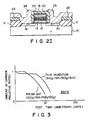
- Fig. 1 is a cross-sectional view of an ultraviolet erasure type EPROM cell, to which the present invention has been applied.
- a field oxide film 11 for defining a device region is formed in a surface area of a p-type silicon substrate 10.
- a thermal oxide film 12 is formed in the device region defined by the field oxide film 11.
- a floating gate electrode 13 of polycrystalline silicon is formed on the thermal oxide film 12.
- a control gate electrode 18 is formed on the silicon oxide film 17.
- the silicon oxide film 15 is formed by oxidizing the silicon nitride film 14, the quality of the silicon oxide film 15 is excellent and the charge (carrier) retaining property thereof is enhanced.
- the silicon nitride film 14 have a small thickness, namely, 60 ⁇ or less, so that the injection of holes from the control gate electrode 18 into the silicon nitride film 14 can be prevented as much as possible.
- the silicon oxide film 15 have a thickness of 50 ⁇ or more, in order for the silicon nitride film 16 to have a sufficient energy gap and in order to prevent tunneling of carriers through the silicon nitride film 16.
- the silicon nitride film 16 have a thickness of 70 ⁇ or more in order to suppress leakage of electrons from the floating gate electrode 13 and have a thickness of 150 ⁇ or less in order to prevent holes from entering from the control gate electrode 18 into the silicon nitride film 16.
- the silicon oxide film 17 have a thickness of 20 ⁇ or more in order to prevent holes from entering from the control gate electrode 18 into the silicon oxide film 17.
- a source region 19 and a drain region 20 are formed in the device region of the substrate 10.
- a thin thermal oxide film 22 is formed so as to cover the floating gate electrode 13 and the control gate electrode 18.
- a CVD (chemical vapor deposition) oxide film 23 of a predetermined pattern for defining a source contact hole and a drain contact hole is formed as a passivation film on the semiconductor structure.
- a source electrode 24 is formed on the source region 19 and a drain electrode 25 is formed on the drain region 20, respectively, through the source contact hole and the drain contact hole formed in the CVD oxide film 23.
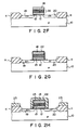
- Figs. 2A to 2I are cross-sectional views for illustrating a process for manufacturing the ultraviolet erasure type EPROM cell shown in Fig. 1.
- the same elements as appear in Fig. 1 are denoted by the same reference numerals.
- a field oxide film 11 for defining a device region is formed in a surface portion of a p-type silicon substrate 10 by a selective oxidation method.
- the resultant body is subjected to a thermal treatment at about 900°C, whereby a thermal oxide film 112 with a thickness of about 200 ⁇ , a portion of which becomes a first gate insulating film 12, is formed on the device region of the substrate 10.
- a first polycrystalline silicon film 113 with a thickness of about 4000 ⁇ , a portion of which becomes a floating gate electrode 13, is formed on the semiconductor structure by means of a CVD (chemical vapor deposition) process.
- CVD chemical vapor deposition
- Phosphorus is then diffused in the first polycrystalline silicon film 113 at about 900°C, with POCl3 being used as a diffusion source.
- a first silicon nitride film 114 with a thickness of about 110 ⁇ is formed on the first polycrystalline silicon film 113, for example, by means of an LP (low pressure) CVD method.
- the silicon nitride film 114 is oxidized by a burning oxidation method, and a first silicon oxide film 115 with a thickness of about 90 ⁇ is formed on the silicon nitride film 114.
- the silicon nitride film 114 is consumed by about 60 ⁇ and the thickness thereof becomes about 50 ⁇ .
- a second silicon nitride film 116 with a thickness of about 120 ⁇ is formed on the silicon oxide film 115, for example, by means of the LPCVD method.
- the second silicon nitride film 116 is oxidized by a burning oxidation method, and a second silicon oxide film 117 with a thickness of about 30 ⁇ is formed on the silicon nitride film 116.
- the silicon nitride film 116 is consumed by about 20 ⁇ , and the thickness thereof becomes about 100 ⁇ .
- an interlayer insulating film of a four-layer structure wherein the silicon nitride film 114, silicon oxide film lls, silicon nitride film 116 and silicon oxide film 117 are laminated in this order, is formed on the polycrystalline silicon film 113.
- the second polycrystalline silicon film 118, silicon oxide film 117, silicon nitride film 116, silicon oxide film 115, silicon nitride film 114, first polycrystalline silicon film 113, and thermal oxide film 112 are selectively etched in this order by means of a photoetching method.
- the floating gate electrode 13 which is a part of the first polycrystalline silicon film 113, is formed on the substrate 10, with the first gate insulating film 12, which is a part of the thermal oxide film 112, being interposed between the floating gate electrode 13 and the substrate 10.
- arsenic is ion-implanted in the substrate 10 with the control gate electrode 18 used as a mask, thus forming n+type source and drain regions 19 and 20 in a surface portion of the substrate 10, as shown in Fig. 2F.
- the semiconductor structure is subjected to thermal oxidation at about 950°C in a dry oxidation atmosphere, to form a thermal oxide film with a thickness of 400 ⁇ .
- This thermal oxide film is selectively etched in a predetermined pattern, thus forming a thermal oxide film 22 with a thickness of 400 ⁇ on the surfaces of the floating gate electrode 13 and the control gate electrode 18, as shown in Fig. 2G.
- Contact holes are formed in the CVD oxide film 23 by means of a photoetching method, as shown in Fig. 2H.
- An alloy film formed of aluminum and silicon, with a thickness of 1.0 ⁇ m, is formed on the semiconductor structure by means of the CVD method.
- the alloy film is patterned, and a source electrode 24 is formed on the source region 19 and a drain electrode 25 is formed on the drain region 20, as shown in Fig. 2I.
- the EPROM shown in Fig. 1 is formed.
- Fig. 3 shows the amounts of retained carriers in the case where the EPROM cell of the present invention as shown in Fig. 1 and a conventional EPROM cell are left at a high temperature of 300°C.
- the conventional EPROM cell in the initial several hours, has a greater amount of retained carriers than the EPROM cell of the present invention. However, thereafter, the amount of retained carriers in the EPROM of the present invention becomes remarkably greater.
Landscapes
- Non-Volatile Memory (AREA)
- Semiconductor Memories (AREA)
Applications Claiming Priority (2)
| Application Number | Priority Date | Filing Date | Title |
|---|---|---|---|
| JP1008006A JPH07118511B2 (ja) | 1989-01-17 | 1989-01-17 | 不揮発性半導体記憶装置 |
| JP8006/89 | 1989-01-17 |
Publications (3)
| Publication Number | Publication Date |
|---|---|
| EP0383011A2 true EP0383011A2 (fr) | 1990-08-22 |
| EP0383011A3 EP0383011A3 (en) | 1990-12-12 |
| EP0383011B1 EP0383011B1 (fr) | 1996-03-13 |
Family
ID=11681271
Family Applications (1)
| Application Number | Title | Priority Date | Filing Date |
|---|---|---|---|
| EP90100445A Expired - Lifetime EP0383011B1 (fr) | 1989-01-17 | 1990-01-10 | Dispositif semi-conducteur de mémoire rémanente |
Country Status (4)
| Country | Link |
|---|---|
| EP (1) | EP0383011B1 (fr) |
| JP (1) | JPH07118511B2 (fr) |
| KR (1) | KR930001888B1 (fr) |
| DE (1) | DE69025784T2 (fr) |
Cited By (5)
| Publication number | Priority date | Publication date | Assignee | Title |
|---|---|---|---|---|
| DE4241457A1 (fr) * | 1991-12-10 | 1993-06-17 | Micron Technology Inc | |
| EP0571692A1 (fr) * | 1992-05-27 | 1993-12-01 | STMicroelectronics S.r.l. | Cellule EPROM ayant un isolant entre couches de polysilicium facilement réalisable en petites dimensions |
| US5661056A (en) * | 1994-09-29 | 1997-08-26 | Nkk Corporation | Non-volatile semiconductor memory device and method of manufacturing the same |
| DE19752434C2 (de) * | 1997-03-10 | 2000-10-19 | Mitsubishi Electric Corp | Nichtflüchtige Halbleiterspeichervorrichtung mit einer p-Typ dotierten Gateelektrode mit schwebendem Potential |
| US7306990B2 (en) * | 2002-11-29 | 2007-12-11 | Japan Science & Technology Agency | Information storage element, manufacturing method thereof, and memory array |
Families Citing this family (3)
| Publication number | Priority date | Publication date | Assignee | Title |
|---|---|---|---|---|
| JPH09134973A (ja) * | 1995-11-07 | 1997-05-20 | Mitsubishi Electric Corp | 半導体装置およびその製造方法 |
| KR19990057077A (ko) * | 1997-12-29 | 1999-07-15 | 구본준 | 비휘발성 메모리 소자 제조방법 |
| JP4342621B2 (ja) | 1998-12-09 | 2009-10-14 | 株式会社東芝 | 不揮発性半導体記憶装置 |
Family Cites Families (1)
| Publication number | Priority date | Publication date | Assignee | Title |
|---|---|---|---|---|
| JPS61136274A (ja) * | 1984-12-07 | 1986-06-24 | Toshiba Corp | 半導体装置 |
-
1989
- 1989-01-17 JP JP1008006A patent/JPH07118511B2/ja not_active Expired - Fee Related
- 1989-12-22 KR KR1019890019284A patent/KR930001888B1/ko not_active Expired - Fee Related
-
1990
- 1990-01-10 EP EP90100445A patent/EP0383011B1/fr not_active Expired - Lifetime
- 1990-01-10 DE DE69025784T patent/DE69025784T2/de not_active Expired - Fee Related
Cited By (9)
| Publication number | Priority date | Publication date | Assignee | Title |
|---|---|---|---|---|
| DE4241457A1 (fr) * | 1991-12-10 | 1993-06-17 | Micron Technology Inc | |
| DE4241457B4 (de) * | 1991-12-10 | 2006-05-24 | Micron Technology, Inc. | P-leitendes floatendes Gate aus Poly-Silizium zur Verwendung bei einem Halbleiterbautransistorelement und daraus hergestelltes Flash-E2PROM |
| EP0571692A1 (fr) * | 1992-05-27 | 1993-12-01 | STMicroelectronics S.r.l. | Cellule EPROM ayant un isolant entre couches de polysilicium facilement réalisable en petites dimensions |
| US5422291A (en) * | 1992-05-27 | 1995-06-06 | Sgs-Thomson Microelectronics, S.R.L. | Method of making an EPROM cell with a readily scalable interpoly dielectric |
| US5600166A (en) * | 1992-05-27 | 1997-02-04 | Sgs-Thomson Microelectronics, S.R.L. | EPROM cell with a readily scalable interpoly dielectric |
| US5661056A (en) * | 1994-09-29 | 1997-08-26 | Nkk Corporation | Non-volatile semiconductor memory device and method of manufacturing the same |
| US5907183A (en) * | 1994-09-29 | 1999-05-25 | Nkk Corporation | Non-volatile semiconductor memory device |
| DE19752434C2 (de) * | 1997-03-10 | 2000-10-19 | Mitsubishi Electric Corp | Nichtflüchtige Halbleiterspeichervorrichtung mit einer p-Typ dotierten Gateelektrode mit schwebendem Potential |
| US7306990B2 (en) * | 2002-11-29 | 2007-12-11 | Japan Science & Technology Agency | Information storage element, manufacturing method thereof, and memory array |
Also Published As
| Publication number | Publication date |
|---|---|
| KR930001888B1 (ko) | 1993-03-19 |
| JPH07118511B2 (ja) | 1995-12-18 |
| KR900012338A (ko) | 1990-08-03 |
| JPH02188970A (ja) | 1990-07-25 |
| EP0383011A3 (en) | 1990-12-12 |
| DE69025784D1 (de) | 1996-04-18 |
| DE69025784T2 (de) | 1996-08-08 |
| EP0383011B1 (fr) | 1996-03-13 |
Similar Documents
| Publication | Publication Date | Title |
|---|---|---|
| US5304829A (en) | Nonvolatile semiconductor device | |
| US5629222A (en) | Method of forming semiconductor memory device by selectively forming an insulating film on the drain region | |
| KR910007377B1 (ko) | 반도체장치 | |
| US6274902B1 (en) | Nonvolatile floating gate memory with improved interpoly dielectric | |
| KR100239459B1 (ko) | 반도체 메모리 소자 및 그 제조방법 | |
| KR0138312B1 (ko) | 비휘발성 반도체 메모리장치의 제조방법 | |
| US5200636A (en) | Semiconductor device having E2 PROM and EPROM in one chip | |
| US5658812A (en) | Nonvolatile semiconductor memory device and its manufacturing method | |
| US6417044B1 (en) | Non-volatile memory and memory of manufacturing the same | |
| US6608347B2 (en) | Semiconductor device and method of manufacturing the same | |
| US5880498A (en) | Semiconductor device having a nitrogen doped polysilicon layer | |
| KR0124629B1 (ko) | 불휘발성 반도체 메모리장치의 제조방법 | |
| EP0383011B1 (fr) | Dispositif semi-conducteur de mémoire rémanente | |
| US6380584B1 (en) | Semiconductor memory device with single and double sidewall spacers | |
| US6891222B2 (en) | Non-volatile memory devices and methods of fabricating the same | |
| US5208173A (en) | Method of manufacturing non-volatile semiconductor memory device | |
| KR920001640B1 (ko) | 불휘발성 반도체장치 | |
| JP3526090B2 (ja) | 半導体装置の製造方法 | |
| USRE40275E1 (en) | Method for producing a memory cell | |
| JPH02277269A (ja) | 不揮発性メモリ装置の製造方法 | |
| JP2733972B2 (ja) | 半導体集積回路装置の製造方法 | |
| JPH11297863A (ja) | コンタクトレスアレイ構成の不揮発性メモリおよびその製造方法 | |
| JPH05251712A (ja) | 不揮発性半導体記憶装置の製造方法 | |
| JPH0936258A (ja) | 半導体装置およびその製造方法 | |
| JPH11126833A (ja) | 不揮発性半導体記憶装置及びその製造方法 |
Legal Events
| Date | Code | Title | Description |
|---|---|---|---|
| PUAI | Public reference made under article 153(3) epc to a published international application that has entered the european phase |
Free format text: ORIGINAL CODE: 0009012 |
|
| 17P | Request for examination filed |
Effective date: 19900110 |
|
| AK | Designated contracting states |
Kind code of ref document: A2 Designated state(s): DE FR GB |
|
| PUAL | Search report despatched |
Free format text: ORIGINAL CODE: 0009013 |
|
| AK | Designated contracting states |
Kind code of ref document: A3 Designated state(s): DE FR GB |
|
| 17Q | First examination report despatched |
Effective date: 19930707 |
|
| GRAA | (expected) grant |
Free format text: ORIGINAL CODE: 0009210 |
|
| AK | Designated contracting states |
Kind code of ref document: B1 Designated state(s): DE FR GB |
|
| REF | Corresponds to: |
Ref document number: 69025784 Country of ref document: DE Date of ref document: 19960418 |
|
| ET | Fr: translation filed | ||
| PLBE | No opposition filed within time limit |
Free format text: ORIGINAL CODE: 0009261 |
|
| STAA | Information on the status of an ep patent application or granted ep patent |
Free format text: STATUS: NO OPPOSITION FILED WITHIN TIME LIMIT |
|
| 26N | No opposition filed | ||
| PGFP | Annual fee paid to national office [announced via postgrant information from national office to epo] |
Ref country code: GB Payment date: 19980102 Year of fee payment: 9 |
|
| PGFP | Annual fee paid to national office [announced via postgrant information from national office to epo] |
Ref country code: FR Payment date: 19980109 Year of fee payment: 9 |
|
| PG25 | Lapsed in a contracting state [announced via postgrant information from national office to epo] |
Ref country code: GB Free format text: LAPSE BECAUSE OF NON-PAYMENT OF DUE FEES Effective date: 19990110 |
|
| GBPC | Gb: european patent ceased through non-payment of renewal fee |
Effective date: 19990110 |
|
| PG25 | Lapsed in a contracting state [announced via postgrant information from national office to epo] |
Ref country code: FR Free format text: LAPSE BECAUSE OF NON-PAYMENT OF DUE FEES Effective date: 19990930 |
|
| REG | Reference to a national code |
Ref country code: FR Ref legal event code: ST |
|
| PGFP | Annual fee paid to national office [announced via postgrant information from national office to epo] |
Ref country code: DE Payment date: 20070104 Year of fee payment: 18 |
|
| PG25 | Lapsed in a contracting state [announced via postgrant information from national office to epo] |
Ref country code: DE Free format text: LAPSE BECAUSE OF NON-PAYMENT OF DUE FEES Effective date: 20080801 |