EP0383300A2 - Dielektrisches Filter des LC-Typs - Google Patents
Dielektrisches Filter des LC-Typs Download PDFInfo
- Publication number
- EP0383300A2 EP0383300A2 EP90102896A EP90102896A EP0383300A2 EP 0383300 A2 EP0383300 A2 EP 0383300A2 EP 90102896 A EP90102896 A EP 90102896A EP 90102896 A EP90102896 A EP 90102896A EP 0383300 A2 EP0383300 A2 EP 0383300A2
- Authority
- EP
- European Patent Office
- Prior art keywords
- coupling
- dielectric
- dielectric plate
- strip line
- circuit
- Prior art date
- Legal status (The legal status is an assumption and is not a legal conclusion. Google has not performed a legal analysis and makes no representation as to the accuracy of the status listed.)
- Granted
Links
- 230000008878 coupling Effects 0.000 claims abstract description 38
- 238000010168 coupling process Methods 0.000 claims abstract description 38
- 238000005859 coupling reaction Methods 0.000 claims abstract description 38
- 230000001939 inductive effect Effects 0.000 claims description 11
- 239000004020 conductor Substances 0.000 claims 1
- 238000004519 manufacturing process Methods 0.000 abstract description 7
- 239000003990 capacitor Substances 0.000 description 30
- 239000003989 dielectric material Substances 0.000 description 11
- 239000000919 ceramic Substances 0.000 description 9
- 239000002184 metal Substances 0.000 description 8
- 238000012986 modification Methods 0.000 description 8
- 230000004048 modification Effects 0.000 description 8
- 238000007747 plating Methods 0.000 description 6
- 230000003071 parasitic effect Effects 0.000 description 5
- 239000000463 material Substances 0.000 description 4
- 238000004891 communication Methods 0.000 description 3
- 238000010586 diagram Methods 0.000 description 3
- 239000004593 Epoxy Substances 0.000 description 2
- 238000004458 analytical method Methods 0.000 description 2
- 238000005516 engineering process Methods 0.000 description 2
- 239000003822 epoxy resin Substances 0.000 description 2
- 238000002474 experimental method Methods 0.000 description 2
- 238000000034 method Methods 0.000 description 2
- 238000010295 mobile communication Methods 0.000 description 2
- 229920000647 polyepoxide Polymers 0.000 description 2
- 238000009966 trimming Methods 0.000 description 2
- HMDDXIMCDZRSNE-UHFFFAOYSA-N [C].[Si] Chemical compound [C].[Si] HMDDXIMCDZRSNE-UHFFFAOYSA-N 0.000 description 1
- 230000001413 cellular effect Effects 0.000 description 1
- 238000007796 conventional method Methods 0.000 description 1
- 238000011161 development Methods 0.000 description 1
- 238000011031 large-scale manufacturing process Methods 0.000 description 1
- 238000011160 research Methods 0.000 description 1
- 230000035945 sensitivity Effects 0.000 description 1
Images


Classifications
-
- H—ELECTRICITY
- H01—ELECTRIC ELEMENTS
- H01P—WAVEGUIDES; RESONATORS, LINES, OR OTHER DEVICES OF THE WAVEGUIDE TYPE
- H01P1/00—Auxiliary devices
- H01P1/20—Frequency-selective devices, e.g. filters
- H01P1/201—Filters for transverse electromagnetic waves
- H01P1/205—Comb or interdigital filters; Cascaded coaxial cavities
- H01P1/2056—Comb filters or interdigital filters with metallised resonator holes in a dielectric block
Definitions
- This invention relates to an LC-type dielectric filter utilized in microwave band communication and more particularly to an LC-type dielectric filter using strip lines for resonators.
- Fig. 1 illustrates a four resonator type uni-block dielectric filter disclosed in the above mentioned article.
- the filter comprises a single rectangular dielectric block D1.
- the dielectric block D1 has four cylindrical holes H1 to H4 having metalized interior surfaces and metalized portions M1 to M10 on the block surfaces.
- each of the holes performs as a short-circuited 1/4 wave length coaxial resonator
- the respective spaces between the metalized potions M3, M5, and M7, and the metalized portions M2, M4, and M6 connected to each of the adjacent holes perform the function of coupling capacitances between the resonators.
- Fig. 2(a) and Fig. 2(b) illustrate another example of a conventional dielectric filter disclosed in Japanese Kokai publication No.62-265658 published on November 18, 1987, wherein Fig. 2(a) illustrates a front side of the filter and Fig. 2(b) illustrates a reverse side of the filter.
- a main body of the filter comprises a dielectric plate D2 having four through holes H5 to H8. Further, on the front side of the dielectric plate D2, there are provided three spiral printed coils L 1A , L 2A , and L 3A for inductance of the filter and three metalized portions C 1A , C 2A , and C 3A for capacitance of the filter. Each of the inductances and capacitances is electrically combined with a corresponding similar configuration provided on the reverse side of the dielectric plate D2.
- Fig. 2 (b) on the reverse side of the dielectric plate D2, there are provided four metalized portion C 1B , C 2B-1 , C 2B-2 , and C 3B which are coupled with the above mentioned metalized portions C 1A , C 2A , and C 3A via the dielectric material of the dielectric plate D2 for forming capacitors of the filter. Further, there are provided three printed coils L 1B , L 2B , and L 3B for forming inductance of the filter. According to this configuration, because the diameters of the coils on each side are different, the parasitic capacitance between the coils can be reduced and the frequency characteristic of the filter can be improved, as is described in detail in the Japanese Kokai Publication.
- the quality factor of this kind of filter when not loaded may be up to approximately 100. This is why the filter is applicable for use only under the approximately 500 MHz frequency band. If the frequency exceeds 500 MHz, the parasitic impedance increases at an approximately exponential rate and it cannot satisfy the necessary frequency characteristic.
- An object of the invention is to provide a small and high-Q LC-type dielectric filter featuring a plurality of parallel LC-type resonators which are comprised of strip lines.
- Another object of the invention is to provide an LC-type dielectric filter which is suitable for mass-production because all of elements of the filter are manufacturable by metal plating on a dielectric plate.
- the LC-type filter according to the invention comprises a single dielectric plate on which is formed a printed circuit which includes a conductive layer forming a ground portion, an input terminal, an output terminal, at least first and second strip lines forming a pair of distributed constant resonators, one end of each of the strip lines being connected to the ground portion, a first coupling circuit coupling the other end of the first strip line and the input terminal, a second coupling circuit coupling the other end of the second strip line and the output terminal, and at least one third coupling circuit coupling together the other ends of the first and second strip lines.
- each of the strip lines is provided by plating as a distributed constant resonator circuit, such as a 1/2 or 1/4 wave length resonator.
- a strip line circuit on a dielectric material is low-loss and has a high quality factor. Therefore, it becomes possible to realize a small and high-Q filter.
- circuit elements such as coupling capacitances, connecting electrodes, and input/output terminals provided as plated through holes, can be easily provided by the same process, it becomes easy to make a dielectric filter which is suitable for mass-production.
- the dielectric plate D3 is made of a glass-epoxy resin and has a thickness of 1.0 mm. Such a plate has a relatively low dielectric constant (specific inductive capacitance) ⁇ r of approximately 4.5.
- dielectric plate D3 On the dielectric plate D3, there are plated metalized portions 12, 12′ to function as ground. Further, all of the side surfaces (one of which is shown in Fig. 3(b)) are also metalized to reduce filter loss and to improve the frequency characteristic.
- Five metal plated through holes including an input terminal IN, an output terminal OUT and three additional through holes 20, are provided for electrical connection.
- the terminals and three additional through holes extend from the upper surface to the reverse surface of the dielectric plate D3.
- capacitors 15 and 17 have the same value of capacitance C0 and the capacitor 19 has a value of capacitance C4. In this way, there can be provided relatively high capacitance capacitors.
- the capacitors 25 and 33 have the same value of capacitance C12.
- the capacitor 29 has a value of capacitance C23.
- the capacitances of capacitors 25, 29 and 33 are smaller than those of capacitances 15, 17, and 19 and are therefore provided in different configurations.
- strip line a strip form electrode
- Fig. 3(e) which illustrates a bottom surface of a resonator, a part of the bottom surface opposite to the metalized portion 12 and left and right surfaces of the dielectric block are fully metalized to contact the metalized portion 12 for grounding and an improved frequency characteristic.
- the only portion of the bottom surface which is not metalized is an exposed portion 39 at one end of the strip line 38-n, which is provided to avoid short circuiting of the resonator.
- Fig. 3(d) which is a sectional view of the filter in a plane through the dielectric plate D3 and a resonator
- one end of each of the strip lines 38-n is connected to the corresponding printed circuit 34 at a location adjacent to the back surface of the corresponding block 36-n via a soldered portion 35, and the other end of each of the strip lines 38-n is also connected to the metalized portion 12 for grounding.
- the dielectric material used in the dielectric blocks is dielectric ceramic which has a dielectric constant of approximately 75.
- a relatively low dielectric constant material such as glass-epoxy resin is used for the printed circuit board including capacitors, and the relatively high dielectric constant material such as ceramics is used only for the resonators themselves which should have a high dielectric constant. This of course reduces the overall cost in comparison with the conventional single dielectric plate filter formed of the more expensive ceramics, such as illustrated in Figs 2(a) and 2(b).
- the length of the strip lines 38-n is one fourth of the wave length of the applied frequency for resonance.
- the following is an analysis of the filter of the invention.
- This circuit resonates at an angular frequency ⁇ c which satisfy the following equation:
- the input impedance Z in becomes infinite.
- the strip line becomes equivalent to a parallel resonator circuit and satisfies the following equation: where, L c and C c represent an inductance component and a capacitance component respectively of the equivalent circuit of the parallel resonator circuit. According to this relation, with the strip line short circuited the equivalent becomes that of a primarily inductive resonator circuit below the resonant frequency. Further, L c , C c , Z0 and ⁇ l satisfy the following relations.
- the equation for the inductance L of a parallel LC circuit is given by L c (1- ⁇ 2L c C c ).
- the equivalent circuit becomes a capacitance circuit.
- the equivalent circuit of the open circuited strip line is a series resonator circuit which is primarily capacitive at input frequencies under the resonant frequency ⁇ c .
- L c , C c , Z0, and ⁇ l have the following relations.
- A is the area of the capacitor plates (cm2)
- t is the distance between the plates (cm)
- ⁇ r is the specific inductive capacity of the dielectric material between the plates.
- ⁇ r is 4.5 and t is 0.1 cm
- A is 0.45 cm2 (0.67 cm by 0.67 cm)
- the capacitance of each capacitor is about 1.72 pF.
- the distance t in the above equation is equivalent to a perpendicular distance between the line-shaped electrodes.
- the area A is 0.025 cm2 (1.25 cm by 0.02 cm) and the distance t is 0.02 cm, and therefore the capacitance is about 0.49 pF.
- the capacitor 29 comprising a pair of electrodes (26, 28)
- the area A is 0.039 cm2 (0.962 cm by 0.02 cm) and the distance t is 0.02 cm, and therefore the capacitance is 0.37 pF.
- the equivalent circuit of the first embodiment has a circuit diagram as shown in Fig. 5.
- the volume of the first embodiment of the invention is almost half that of the above described first example of a conventional filter, which is illustrated in Fig. 1.
- the Q (Quality factor) of the first embodiment of the invention is approximately 500, which is a sufficient value to be used in 800 MHz band mobile communications.
- Fig. 4(a) is an exploded partial sectional view of a modification of the first embodiment.
- the circuit will be a relatively low-loss circuit.
- a separate dielectric plate 40 which has approximately the same size as the dielectric block and all of whose surfaces except the bottom, front, and back surfaces are covered with a plating 40a.
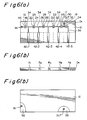
- Fig. 6(a), Fig. 6(b), and Fig. 6(c) illustrate a second embodiment of the invention.
- the same reference numerals denote the same or equivalent elements as illustrated in Fig. 3(a), 3(b), and 3(c).
- the glass-epoxy circuit board D3 featured in the first embodiment is replaced with a ceramic dielectric plate D4 which has relatively high specific inductive capacitance.
- the higher specific inductive capacity dielectric material is more costly, so the cost of the filter will therefore increase since the embodiment requires a great amount of the more expensive dielectric material.
- the reverse side of the dielectric plate D4 is entirely covered by a metalized portion 12 except two exposed portions 56 and 58 around the input terminal IN and the output terminal OUT.
- the coupling capacitors 15 and 17, that is, the capacitors having capacitances C0 and the capacitor 19, that is the capacitor having the caspacitance C4 can be made in the same way as the other coupling capacitors including the two capacitors 25 and 33 having the capacitance C12 and the capacitor 29 having the capacitance C23.
- Fig. 7(a) and Fig. 7(b) illustrate a modification of the second embodiment of the invention similar to that shown in Figs. 4(a) and 4(b).
- the entire dielectric plate D4 is covered by a ceramic dielectric plate 60 which is approximately the same size as the dielectric plate D4 and all of whose surfaces except the front and bottom surfaces are covered with metal plating 60a. According to this modification, there can be obtained a low-loss, high-Q filter.
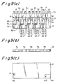
- Fig. 8(a), Fig. 8(b), and Fig. 8(c) illustrate a third embodiment of the invention.
- an equivalent circuit of this embodiment is the same equivalent circuit as that for the other embodiments, which is illustrated in Fig. 5.
- An advantage of this embodiment is that it is easy to perform fine tuning of each components of the resonators by trimming.
- Fig. 9(a), Fig. 9(b), and Fig. 9(c) illustrate a fourth embodiment of the invention.
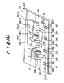
- Fig. 10 illustrate a fifth embodiment of the invention
- Fig. 11 illustrates an equivalent circuit of the fifth embodiment
- the filter according to this embodiment comprises a combination of a rectangular coaxial resonator 76 corresponding to L1 and C1 in Fig. 11, a glass-epoxy dielectric plate D5, a resonator 78-1 corresponding to L2 and C2, and a resonator 78-2 corresponding to L3 and C3, resonators 78-1 and 78-2 are the same resonators as in Fig. 3(a) for the first embodiment of the invention.
- the coaxial resonator 76 is a conventional type dielectric resonator and includes a relatively large dielectric ceramic block 84 having a through hole 86 whose interior surface is metalized. As shown in Fig. 10, the entire surface of the block 84 except its front surface is metal plated and the interior metalized portion is connected to coupling capacitors 91 and 95 via printed circuit 34.
- each of the other coupling capacitors including capacitor 95 of capacitance C1, capacitor 99 of capacitance C2, and capacitor 103 of capacitance C0 is comprised of a combination of a pair of printed line electrodes, 88 and 90, 92 and 94, 96 and 98, and 100 and 102 respectively.
- the coaxial resonator Since the coaxial resonator has a relatively higher quality factor than the strip line resonator, it would be able to realize a high Q filter.
Landscapes
- Physics & Mathematics (AREA)
- Electromagnetism (AREA)
- Control Of Motors That Do Not Use Commutators (AREA)
- Networks Using Active Elements (AREA)
- Filters And Equalizers (AREA)
Applications Claiming Priority (4)
| Application Number | Priority Date | Filing Date | Title |
|---|---|---|---|
| JP3512989A JPH02215201A (ja) | 1989-02-16 | 1989-02-16 | Lc形ろ波器 |
| JP35129/89 | 1989-02-16 | ||
| JP312370/89 | 1989-12-01 | ||
| JP31237089A JPH03173201A (ja) | 1989-12-01 | 1989-12-01 | ハイブリッドフィルタ |
Publications (3)
| Publication Number | Publication Date |
|---|---|
| EP0383300A2 true EP0383300A2 (de) | 1990-08-22 |
| EP0383300A3 EP0383300A3 (de) | 1991-05-29 |
| EP0383300B1 EP0383300B1 (de) | 1994-12-07 |
Family
ID=26374055
Family Applications (1)
| Application Number | Title | Priority Date | Filing Date |
|---|---|---|---|
| EP90102896A Expired - Lifetime EP0383300B1 (de) | 1989-02-16 | 1990-02-14 | Dielektrisches Filter des LC-Typs |
Country Status (4)
| Country | Link |
|---|---|
| US (1) | US5124675A (de) |
| EP (1) | EP0383300B1 (de) |
| DE (1) | DE69014674T2 (de) |
| NO (1) | NO176298C (de) |
Cited By (2)
| Publication number | Priority date | Publication date | Assignee | Title |
|---|---|---|---|---|
| EP0413211A3 (en) * | 1989-08-14 | 1991-06-12 | Oki Electric Industry Co., Ltd. | Microstrip line type resonator |
| USD805476S1 (en) * | 2016-12-20 | 2017-12-19 | Cirocomm Technology Corp. | Dielectric filter |
Families Citing this family (16)
| Publication number | Priority date | Publication date | Assignee | Title |
|---|---|---|---|---|
| US5313662A (en) * | 1990-07-26 | 1994-05-17 | Motorola, Inc. | Split-ring resonator bandpass filter with adjustable zero |
| FI87854C (fi) * | 1991-04-12 | 1993-02-25 | Lk Products Oy | Foerfarande foer att tillverka ett hoegfrekvensfilter samt hoegfrekvensfilter tillverkat enligt foerfarandet |
| US5300903A (en) * | 1991-06-27 | 1994-04-05 | Murata Manufacturing Co., Ltd. | Band-pass filter |
| FI95179C (fi) * | 1993-11-01 | 1995-12-27 | Verdera Oy | Liuskajohtoresonaattorirakenne |
| US5497337A (en) * | 1994-10-21 | 1996-03-05 | International Business Machines Corporation | Method for designing high-Q inductors in silicon technology without expensive metalization |
| DE19652799C2 (de) * | 1996-12-18 | 1999-05-20 | Siemens Ag | Mikrowellenfilter |
| JP3712095B2 (ja) * | 1998-01-14 | 2005-11-02 | 株式会社村田製作所 | 入出力バランス型フィルタ |
| ITMI981563A1 (it) * | 1998-07-09 | 2000-01-09 | Alsthom Cge Alcatel | Dispositivo comprendente un risonatore dielettrico coassiale montato su microstriscia a basso rumore di fase e metodo per ridurre il |
| FI115331B (fi) * | 2000-09-22 | 2005-04-15 | Filtronic Comtek Oy | Ylipäästösuodatin |
| US6813124B1 (en) * | 2002-06-21 | 2004-11-02 | Lionel L.L.C. | Transformer over-current protection with RMS sensing and voltage fold-back |
| US7471170B2 (en) * | 2003-03-21 | 2008-12-30 | Nxp B.V. | Multilayer stack with compensated resonant circuit |
| JP4933733B2 (ja) * | 2005-01-11 | 2012-05-16 | 株式会社アドバンテスト | 信号伝送システム、信号出力回路基板、信号受信回路基板、信号出力方法、及び信号受信方法 |
| JP4770801B2 (ja) * | 2007-06-26 | 2011-09-14 | 横河電機株式会社 | 高周波フィルタ |
| US9136570B2 (en) * | 2007-12-07 | 2015-09-15 | K & L Microwave, Inc. | High Q surface mount technology cavity filter |
| KR101345807B1 (ko) | 2013-05-29 | 2013-12-27 | 주식회사 케오솔 | 유전체 필터 모듈을 이용한 맞춤형 전류 흐름 개선장치 |
| CN107947752A (zh) * | 2017-12-29 | 2018-04-20 | 中国电子科技集团公司第四十三研究所 | 一种带通滤波器 |
Family Cites Families (13)
| Publication number | Priority date | Publication date | Assignee | Title |
|---|---|---|---|---|
| AU470870B2 (en) * | 1973-10-29 | 1976-04-01 | Matsushita Electric Industrial Co., Ltd. | Filters employing elements with distributed constants |
| FR2438937A1 (fr) * | 1978-10-11 | 1980-05-09 | Thomson Csf | Dispositif resonateur pour ondes radioelectriques a accord de frequence electronique et oscillateur a diode a resistance negative incorporant un tel dispositif |
| US4429289A (en) * | 1982-06-01 | 1984-01-31 | Motorola, Inc. | Hybrid filter |
| JPS5927601A (ja) * | 1982-08-05 | 1984-02-14 | Nec Corp | マイクロストリツプ型帯域阻止「ろ」 |
| JPS6065601A (ja) * | 1983-09-21 | 1985-04-15 | Oki Electric Ind Co Ltd | 誘電体フィルタ |
| JPS60114004A (ja) * | 1983-11-25 | 1985-06-20 | Murata Mfg Co Ltd | 誘電体フィルタの実装構造 |
| JPS6128201A (ja) * | 1984-07-18 | 1986-02-07 | Sony Corp | ストリツプ線路フイルタ |
| JPS61208902A (ja) * | 1985-03-13 | 1986-09-17 | Murata Mfg Co Ltd | Mic型誘電体フイルタ |
| JPS6313503A (ja) * | 1986-07-04 | 1988-01-20 | Yuniden Kk | マイクロ波フイルタ装置 |
| JPS63119302A (ja) * | 1986-11-06 | 1988-05-24 | Murata Mfg Co Ltd | ストリツプラインフイルタ |
| JPH0191502A (ja) * | 1987-10-01 | 1989-04-11 | Murata Mfg Co Ltd | 誘電体共振器 |
| JPH02130103U (de) * | 1988-11-16 | 1990-10-26 | ||
| JPH0334305U (de) * | 1989-08-14 | 1991-04-04 |
-
1990
- 1990-02-14 EP EP90102896A patent/EP0383300B1/de not_active Expired - Lifetime
- 1990-02-14 NO NO900707A patent/NO176298C/no unknown
- 1990-02-14 DE DE69014674T patent/DE69014674T2/de not_active Expired - Fee Related
- 1990-09-18 US US07/584,176 patent/US5124675A/en not_active Expired - Lifetime
Cited By (3)
| Publication number | Priority date | Publication date | Assignee | Title |
|---|---|---|---|---|
| EP0413211A3 (en) * | 1989-08-14 | 1991-06-12 | Oki Electric Industry Co., Ltd. | Microstrip line type resonator |
| US5097237A (en) * | 1989-08-14 | 1992-03-17 | Oki Electric Industry Co., Ltd. | Microstrip line type resonator |
| USD805476S1 (en) * | 2016-12-20 | 2017-12-19 | Cirocomm Technology Corp. | Dielectric filter |
Also Published As
| Publication number | Publication date |
|---|---|
| EP0383300B1 (de) | 1994-12-07 |
| DE69014674T2 (de) | 1995-04-27 |
| NO900707L (no) | 1990-08-17 |
| EP0383300A3 (de) | 1991-05-29 |
| NO900707D0 (no) | 1990-02-14 |
| NO176298C (no) | 1995-03-08 |
| US5124675A (en) | 1992-06-23 |
| NO176298B (no) | 1994-11-28 |
| DE69014674D1 (de) | 1995-01-19 |
Similar Documents
| Publication | Publication Date | Title |
|---|---|---|
| EP0383300B1 (de) | Dielektrisches Filter des LC-Typs | |
| US4578656A (en) | Microwave microstrip filter with U-shaped linear resonators having centrally located capacitors coupled to ground | |
| EP0466400B1 (de) | Kopplungstor für einen Resonator mit Mehrfachkondensatoren und mit verteilten Induktoren | |
| US5479141A (en) | Laminated dielectric resonator and dielectric filter | |
| CN110098453B (zh) | 射频滤波器 | |
| US4268809A (en) | Microwave filter having means for capacitive interstage coupling between transmission lines | |
| US5905420A (en) | Dielectric filter | |
| EP0312011B1 (de) | Dielektrisches Filter | |
| US5485131A (en) | Transmission line filter for MIC and MMIC applications | |
| US5812036A (en) | Dielectric filter having intrinsic inter-resonator coupling | |
| EP0638954A1 (de) | Streifenleitungsresonator | |
| JPH0372701A (ja) | 並列多段型帯域通過フィルタ | |
| US4757285A (en) | Filter for short electromagnetic waves formed as a comb line or interdigital line filters | |
| US4631506A (en) | Frequency-adjustable coaxial dielectric resonator and filter using the same | |
| US4754242A (en) | Resonator | |
| KR970000059B1 (ko) | 다중 통과 대역을 가지는 유전 필터 구조 | |
| KR100597094B1 (ko) | 공진기, 필터, 듀플렉서 및 통신 장치 | |
| US4623856A (en) | Incrementally tuned RF filter having pin diode switched lines | |
| JPH0652842B2 (ja) | 有極型誘電体フィルタ | |
| JP2786204B2 (ja) | 帯域阻止フイルタ | |
| US4745379A (en) | Launcher-less and lumped capacitor-less ceramic comb-line filters | |
| US5883554A (en) | Coaxial resonator having coupling electrodes and dielectric filter formed therefrom using the same | |
| JPH07249902A (ja) | ストリップ線路フィルタおよびストリップ線路フィルタとマイクロストリップ線路の接続手段 | |
| US6069543A (en) | Dielectric resonator capable of varying resonant frequency | |
| US5705966A (en) | LC-type dielectric strip line resonator |
Legal Events
| Date | Code | Title | Description |
|---|---|---|---|
| PUAI | Public reference made under article 153(3) epc to a published international application that has entered the european phase |
Free format text: ORIGINAL CODE: 0009012 |
|
| 17P | Request for examination filed |
Effective date: 19900214 |
|
| AK | Designated contracting states |
Kind code of ref document: A2 Designated state(s): DE FR GB SE |
|
| PUAL | Search report despatched |
Free format text: ORIGINAL CODE: 0009013 |
|
| AK | Designated contracting states |
Kind code of ref document: A3 Designated state(s): DE FR GB SE |
|
| 17Q | First examination report despatched |
Effective date: 19931006 |
|
| GRAA | (expected) grant |
Free format text: ORIGINAL CODE: 0009210 |
|
| AK | Designated contracting states |
Kind code of ref document: B1 Designated state(s): DE FR GB SE |
|
| REF | Corresponds to: |
Ref document number: 69014674 Country of ref document: DE Date of ref document: 19950119 |
|
| EAL | Se: european patent in force in sweden |
Ref document number: 90102896.9 |
|
| ET | Fr: translation filed | ||
| PLBE | No opposition filed within time limit |
Free format text: ORIGINAL CODE: 0009261 |
|
| STAA | Information on the status of an ep patent application or granted ep patent |
Free format text: STATUS: NO OPPOSITION FILED WITHIN TIME LIMIT |
|
| 26N | No opposition filed | ||
| PGFP | Annual fee paid to national office [announced via postgrant information from national office to epo] |
Ref country code: FR Payment date: 19980210 Year of fee payment: 9 |
|
| PGFP | Annual fee paid to national office [announced via postgrant information from national office to epo] |
Ref country code: SE Payment date: 19980218 Year of fee payment: 9 |
|
| PG25 | Lapsed in a contracting state [announced via postgrant information from national office to epo] |
Ref country code: SE Free format text: LAPSE BECAUSE OF NON-PAYMENT OF DUE FEES Effective date: 19990215 |
|
| PG25 | Lapsed in a contracting state [announced via postgrant information from national office to epo] |
Ref country code: FR Free format text: LAPSE BECAUSE OF NON-PAYMENT OF DUE FEES Effective date: 19991029 |
|
| EUG | Se: european patent has lapsed |
Ref document number: 90102896.9 |
|
| REG | Reference to a national code |
Ref country code: FR Ref legal event code: ST |
|
| REG | Reference to a national code |
Ref country code: GB Ref legal event code: IF02 |
|
| PGFP | Annual fee paid to national office [announced via postgrant information from national office to epo] |
Ref country code: GB Payment date: 20020213 Year of fee payment: 13 |
|
| PGFP | Annual fee paid to national office [announced via postgrant information from national office to epo] |
Ref country code: DE Payment date: 20020227 Year of fee payment: 13 |
|
| PG25 | Lapsed in a contracting state [announced via postgrant information from national office to epo] |
Ref country code: GB Free format text: LAPSE BECAUSE OF NON-PAYMENT OF DUE FEES Effective date: 20030214 |
|
| PG25 | Lapsed in a contracting state [announced via postgrant information from national office to epo] |
Ref country code: DE Free format text: LAPSE BECAUSE OF NON-PAYMENT OF DUE FEES Effective date: 20030902 |
|
| GBPC | Gb: european patent ceased through non-payment of renewal fee |