EP0384586A2 - Emballage plastique à haute fiabilité pour circuits intégrés - Google Patents
Emballage plastique à haute fiabilité pour circuits intégrés Download PDFInfo
- Publication number
- EP0384586A2 EP0384586A2 EP90300934A EP90300934A EP0384586A2 EP 0384586 A2 EP0384586 A2 EP 0384586A2 EP 90300934 A EP90300934 A EP 90300934A EP 90300934 A EP90300934 A EP 90300934A EP 0384586 A2 EP0384586 A2 EP 0384586A2
- Authority
- EP
- European Patent Office
- Prior art keywords
- leads
- integrated circuit
- palladium
- plated
- solder
- Prior art date
- Legal status (The legal status is an assumption and is not a legal conclusion. Google has not performed a legal analysis and makes no representation as to the accuracy of the status listed.)
- Withdrawn
Links
Images
Classifications
-
- H—ELECTRICITY
- H10—SEMICONDUCTOR DEVICES; ELECTRIC SOLID-STATE DEVICES NOT OTHERWISE PROVIDED FOR
- H10W—GENERIC PACKAGES, INTERCONNECTIONS, CONNECTORS OR OTHER CONSTRUCTIONAL DETAILS OF DEVICES COVERED BY CLASS H10
- H10W70/00—Package substrates; Interposers; Redistribution layers [RDL]
- H10W70/01—Manufacture or treatment
- H10W70/04—Manufacture or treatment of leadframes
-
- H—ELECTRICITY
- H10—SEMICONDUCTOR DEVICES; ELECTRIC SOLID-STATE DEVICES NOT OTHERWISE PROVIDED FOR
- H10W—GENERIC PACKAGES, INTERCONNECTIONS, CONNECTORS OR OTHER CONSTRUCTIONAL DETAILS OF DEVICES COVERED BY CLASS H10
- H10W70/00—Package substrates; Interposers; Redistribution layers [RDL]
- H10W70/40—Leadframes
- H10W70/456—Materials
- H10W70/457—Materials of metallic layers on leadframes
-
- H—ELECTRICITY
- H10—SEMICONDUCTOR DEVICES; ELECTRIC SOLID-STATE DEVICES NOT OTHERWISE PROVIDED FOR
- H10W—GENERIC PACKAGES, INTERCONNECTIONS, CONNECTORS OR OTHER CONSTRUCTIONAL DETAILS OF DEVICES COVERED BY CLASS H10
- H10W72/00—Interconnections or connectors in packages
- H10W72/071—Connecting or disconnecting
- H10W72/075—Connecting or disconnecting of bond wires
- H10W72/07531—Techniques
- H10W72/07532—Compression bonding, e.g. thermocompression bonding
- H10W72/07533—Ultrasonic bonding, e.g. thermosonic bonding
-
- H—ELECTRICITY
- H10—SEMICONDUCTOR DEVICES; ELECTRIC SOLID-STATE DEVICES NOT OTHERWISE PROVIDED FOR
- H10W—GENERIC PACKAGES, INTERCONNECTIONS, CONNECTORS OR OTHER CONSTRUCTIONAL DETAILS OF DEVICES COVERED BY CLASS H10
- H10W72/00—Interconnections or connectors in packages
- H10W72/50—Bond wires
- H10W72/551—Materials of bond wires
- H10W72/552—Materials of bond wires comprising metals or metalloids, e.g. silver
- H10W72/5522—Materials of bond wires comprising metals or metalloids, e.g. silver comprising gold [Au]
-
- H—ELECTRICITY
- H10—SEMICONDUCTOR DEVICES; ELECTRIC SOLID-STATE DEVICES NOT OTHERWISE PROVIDED FOR
- H10W—GENERIC PACKAGES, INTERCONNECTIONS, CONNECTORS OR OTHER CONSTRUCTIONAL DETAILS OF DEVICES COVERED BY CLASS H10
- H10W72/00—Interconnections or connectors in packages
- H10W72/50—Bond wires
- H10W72/551—Materials of bond wires
- H10W72/552—Materials of bond wires comprising metals or metalloids, e.g. silver
- H10W72/5525—Materials of bond wires comprising metals or metalloids, e.g. silver comprising copper [Cu]
-
- H—ELECTRICITY
- H10—SEMICONDUCTOR DEVICES; ELECTRIC SOLID-STATE DEVICES NOT OTHERWISE PROVIDED FOR
- H10W—GENERIC PACKAGES, INTERCONNECTIONS, CONNECTORS OR OTHER CONSTRUCTIONAL DETAILS OF DEVICES COVERED BY CLASS H10
- H10W72/00—Interconnections or connectors in packages
- H10W72/50—Bond wires
- H10W72/59—Bond pads specially adapted therefor
-
- H—ELECTRICITY
- H10—SEMICONDUCTOR DEVICES; ELECTRIC SOLID-STATE DEVICES NOT OTHERWISE PROVIDED FOR
- H10W—GENERIC PACKAGES, INTERCONNECTIONS, CONNECTORS OR OTHER CONSTRUCTIONAL DETAILS OF DEVICES COVERED BY CLASS H10
- H10W72/00—Interconnections or connectors in packages
- H10W72/851—Dispositions of multiple connectors or interconnections
- H10W72/874—On different surfaces
- H10W72/884—Die-attach connectors and bond wires
-
- H—ELECTRICITY
- H10—SEMICONDUCTOR DEVICES; ELECTRIC SOLID-STATE DEVICES NOT OTHERWISE PROVIDED FOR
- H10W—GENERIC PACKAGES, INTERCONNECTIONS, CONNECTORS OR OTHER CONSTRUCTIONAL DETAILS OF DEVICES COVERED BY CLASS H10
- H10W72/00—Interconnections or connectors in packages
- H10W72/90—Bond pads, in general
- H10W72/951—Materials of bond pads
- H10W72/952—Materials of bond pads comprising metals or metalloids, e.g. PbSn, Ag or Cu
-
- H—ELECTRICITY
- H10—SEMICONDUCTOR DEVICES; ELECTRIC SOLID-STATE DEVICES NOT OTHERWISE PROVIDED FOR
- H10W—GENERIC PACKAGES, INTERCONNECTIONS, CONNECTORS OR OTHER CONSTRUCTIONAL DETAILS OF DEVICES COVERED BY CLASS H10
- H10W74/00—Encapsulations, e.g. protective coatings
-
- H—ELECTRICITY
- H10—SEMICONDUCTOR DEVICES; ELECTRIC SOLID-STATE DEVICES NOT OTHERWISE PROVIDED FOR
- H10W—GENERIC PACKAGES, INTERCONNECTIONS, CONNECTORS OR OTHER CONSTRUCTIONAL DETAILS OF DEVICES COVERED BY CLASS H10
- H10W90/00—Package configurations
- H10W90/701—Package configurations characterised by the relative positions of pads or connectors relative to package parts
- H10W90/731—Package configurations characterised by the relative positions of pads or connectors relative to package parts of die-attach connectors
- H10W90/736—Package configurations characterised by the relative positions of pads or connectors relative to package parts of die-attach connectors between a chip and a stacked lead frame, conducting package substrate or heat sink
-
- H—ELECTRICITY
- H10—SEMICONDUCTOR DEVICES; ELECTRIC SOLID-STATE DEVICES NOT OTHERWISE PROVIDED FOR
- H10W—GENERIC PACKAGES, INTERCONNECTIONS, CONNECTORS OR OTHER CONSTRUCTIONAL DETAILS OF DEVICES COVERED BY CLASS H10
- H10W90/00—Package configurations
- H10W90/701—Package configurations characterised by the relative positions of pads or connectors relative to package parts
- H10W90/751—Package configurations characterised by the relative positions of pads or connectors relative to package parts of bond wires
- H10W90/756—Package configurations characterised by the relative positions of pads or connectors relative to package parts of bond wires between a chip and a stacked lead frame, conducting package substrate or heat sink
Definitions
- This invention relates to improved packages for integrated circuit devices and methods for manufacturing improved packages.
- Typical integrated circuit packages are constructed with lead frames made of copper alloy base metals. These lead frames are plated with silver at the terminations of the inner leads to facilitate gold wire bonding from the inner leads to the integrated circuit.
- the lead frame and circuit assemblies are typically encapsulated with an epoxy based plastic mold compound to provide mechanical and corrosion protection for the delicate circuit.
- the adhesive bond between the encapsulation plastic and the inner lead of the lead frame is of low strength and frequently subject to delamination or deterioration. Delamination of the bond between the mold compound and the inner lead frame member provides a potential path for the ingress of moisture and other contaminants that can reach the integrated circuit surface and cause corrosion. Delamination of the lead frame can cause other problems with the mechanical integrity of the package during thermal shock or temperature cycling cracking. These types of problems are becoming more frequent as chip dimensions become larger and package sizes become smaller.
- One specific type of problem, called "popcorn cracking" causes cracks to form after the chip pad becomes delaminated from the mold compound during surface mount solder reflow.
- Another problem with the current assembly technology for integrated circuit packages relates to the method of covering the outer device leads with solder.
- a solder coating is required on the other lead to facilitate soldering to the circuit board in final assembly.
- During package manufacturing the base metal of the lead frame becomes oxidized.
- the soldering process requires the use of corrosive fluxes for dipping or precleaners for solder plating. The presence of residues of these chemicals makes the finished device particularly sensitive to corrosion.
- a high reliability plastic package that includes palladium plated and solder dipped leads for electrical connection to electrical components and support for electrically contacting a semiconductor integrated circuit.
- the present invention provides on the internal leads a palladium surface which is excellent for thermosonic bonding of gold wire to the lead. Such gold wire bonds are equal or better in strength and reliability to prior art bonds made to silver spot inner leads.
- the solder coated external leads of the present invention offer an excellent solderable surface that device end users will have little difficulty accepting.
- the initial palladium surface of the external leads allows for the use of less corrosive chemicals for either the plating activation step or solder dip fluxing. This is because the palladium remains relatively tarnish free and hence the final solder finish is easier to apply by either plating or dipping.
- the primary advantage of the present invention lies in he high adhesive strength associated with palladium to mold compound bonds. This excellent strength is the result of the high surface free energy of palladium. Such surfaces with high free energies present many potential bonding sites to plastic used for molding the package. Direct pull tests of adhesion indicate that palladium plating increases lead frame to mold compound adhesion by approximately 100%. Accelerated reliability testing of the present invention indicates dramatic increases in the expected device life over previous packages. In addition, acoustic microscopy tests have demonstrated that the present invention packages are much less subject to delamination during thermal shock than are prior art packages. These results are supported by additional tests of dye ingression into packages which show the present invention to be superior over prior art packages.
- Another advantage of the present invention is that it will be compatible with the industry wide push to replace the gold bonding wires to copper bonding wires. Tests have shown that copper wire bonds to palladium plated lead frames are simpler to form than similar bonds to either bare or silver plated lead frames.
- the high reliability integrated circuit package of the invention represents a significant increase in the resistance to temperature cycle cracking and moisture related corrosion problems.
- the package is also cost effective.
- the palladium plated lead frame member is manufactured such that it represents only a minimum cost premium over standard silver spot lead frames. This is accomplished through the use of a less than 10 microinch palladium plate. What cost is added can typically be compensated for by the simplification of the solder plate or dip steps. Use of the palladium external leads has been shown to increase the yields during the solder coating steps and hence reduce the overall cost of the package manufacturing.
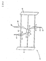
- a lead frame 2 or a plurality of such lead frames connected to each other by connecting strips 4 are prepared for flood plating first with nickel 8 and then with palladium 6.
- Nickel is used to prepare the base metal for the layer of plated palladium.
- the palladium layer 6 and the nickel layer 8 are each deposited in a layer which is substantially uniform in thickness. Thus, no discontinuities in lead frame thickness arise from the plating process.
- Another embodiment of the invention is to replace the palladium layer 6 with a plated layer 6 of palladium-nickel alloy consisting of 80 nickel.
- the palladium plate covers all the surfaces of the lead frame prior to the usual step of trimming excess metal from the lead frame.
- the dam bars 28 are trimmed away after the packaging medium 20 has been applied. Also, adjoining lead frames in a strip of a plurality of lead frames are trimmed to separate them one from the other. After the trimming process is complete, however, the remaining members of the lead frame still have substantially all of their surfaces covered with a layer of palladium.
- the areas of exposed base metal 28 will be, chiefly, the small areas 32 on each external lead 26 where the dam bars 28 have been cut away, and the external lead tips 34 which are cut to separate them from the strip of lead frames.
- the invention embraces palladium plating of lead frames singly or plurally no matter how connected. It will also be appreciated that although palladium flood plating is the preferred method, palladium spot plating or any other plating method is also encompassed by the invention.
- Flood plating is a term well known in the art and refers to plating an entire object by immersion. Spot plating is also a term of art and refers to plating an object in circumscribed areas or spots, as by masking the portions of the object not to be plated.
- the lead frame 2 is comprised of several members, such as the leads 18 and the semiconductor support member 10. Adjacent leads are mechanically connected by dam bars 28. After the packaging medium 20 is in place surrounding all but the external leads 26, the dam bars are removed.
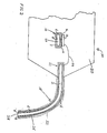
- a palladium plated semiconductor support member 10 is shown with a semiconductor integrated circuit 12 attached by an adhesive 14 to the upper surface 16 of the semiconductor support member.
- the adhesive 14 preferably is electrically conductive to form a good electrical connection between the base of the integrated circuit 12 and the palladium plated upper surface 16 of support member 10.
- lead 18 is supported mechanically by the packaging medium 20, which may be a material such as plastic or ceramic.
- the packaging medium surrounds, protects, and mechanically supports the leads 18, semiconductor support member 10, and integrated circuit 12.
- the lead portion nearest the semiconductor support member 10 is referred to as the lead end 22, and is electrically connected to the integrated circuit 12 via a wire 24 which, typically, is made of gold.
- the gold wire is bonded directly to the palladium plated upper surface of lead end 22, thermosonically or by another suitable technique.
- Thermosonic bonding is a well known technigue and, essentially, consists of a combination of heat and sonic energy delivered via a wand to the combination of metals to be bonded.
- palladium plated external lead 26 protrudes from the packaging medium 20.
- External lead is solder dipped to form a layer of solder 32 using methods well known in the art. This prepares the external leads 26 to be electrically connected to other electrical or electronic parts, such as by soldering or mechanically as with clips or sockets.
- the external leads of the integrated circuit device 30 are connected to components such as resistors, capacitors, other integrated circuit devices, or eguipment such as meters and oscilloscopes for testing purposes.
- the base metal for either of the illustrated embodiments may be chosen from such well known alloys as Alloy 42 which, roughly, is 42% nickel, 58% iron, and small amounts of several other elements; any one of several copper alloys used for lead frames; 400 stainless steel; and copper/stainless steel/copper clad metals. These alloys are well known in the art and are commonly used for lead frame construction.
Landscapes
- Lead Frames For Integrated Circuits (AREA)
- Wire Bonding (AREA)
- Structures Or Materials For Encapsulating Or Coating Semiconductor Devices Or Solid State Devices (AREA)
Applications Claiming Priority (2)
| Application Number | Priority Date | Filing Date | Title |
|---|---|---|---|
| US31376989A | 1989-02-22 | 1989-02-22 | |
| US313769 | 1989-02-22 |
Publications (2)
| Publication Number | Publication Date |
|---|---|
| EP0384586A2 true EP0384586A2 (fr) | 1990-08-29 |
| EP0384586A3 EP0384586A3 (fr) | 1991-03-06 |
Family
ID=23217069
Family Applications (1)
| Application Number | Title | Priority Date | Filing Date |
|---|---|---|---|
| EP19900300934 Withdrawn EP0384586A3 (fr) | 1989-02-22 | 1990-01-30 | Emballage plastique à haute fiabilité pour circuits intégrés |
Country Status (3)
| Country | Link |
|---|---|
| EP (1) | EP0384586A3 (fr) |
| JP (1) | JPH02298056A (fr) |
| KR (1) | KR900013603A (fr) |
Cited By (7)
| Publication number | Priority date | Publication date | Assignee | Title |
|---|---|---|---|---|
| EP0538019A3 (fr) * | 1991-10-17 | 1994-03-09 | Shinko Electric Ind Co | |
| EP0637082A1 (fr) * | 1993-07-29 | 1995-02-01 | AT&T Corp. | Dispositif à circuits intégrés avec cadre de conducteur soudable |
| US5436082A (en) * | 1993-12-27 | 1995-07-25 | National Semiconductor Corporation | Protective coating combination for lead frames |
| US5454929A (en) * | 1994-06-16 | 1995-10-03 | National Semiconductor Corporation | Process for preparing solderable integrated circuit lead frames by plating with tin and palladium |
| US5650661A (en) * | 1993-12-27 | 1997-07-22 | National Semiconductor Corporation | Protective coating combination for lead frames |
| US5728285A (en) * | 1993-12-27 | 1998-03-17 | National Semiconductor Corporation | Protective coating combination for lead frames |
| EP0751564A3 (fr) * | 1995-06-26 | 1998-08-12 | AT&T IPM Corp. | Revêtements d'un métal noble ultra-minces pour empaquetage électronique |
Families Citing this family (2)
| Publication number | Priority date | Publication date | Assignee | Title |
|---|---|---|---|---|
| EP0537982A2 (fr) * | 1991-10-14 | 1993-04-21 | Fujitsu Limited | Dispositif semi-conducteur ayant des conducteurs améliorés |
| JP2673764B2 (ja) * | 1992-07-07 | 1997-11-05 | 株式会社日立製作所 | 樹脂封止型半導体装置 |
Family Cites Families (4)
| Publication number | Priority date | Publication date | Assignee | Title |
|---|---|---|---|---|
| DE3465115D1 (en) * | 1983-05-28 | 1987-09-03 | Masami Kobayashi | Solderable stainless steel article and method for making same |
| JPH0612796B2 (ja) * | 1984-06-04 | 1994-02-16 | 株式会社日立製作所 | 半導体装置 |
| EP0219812A3 (fr) * | 1985-10-25 | 1987-09-30 | Analog Devices, Inc. | Dispositif semi-conducteur encapsulé comprenant des conducteurs externes qu'on peut souder et procédé pour sa fabrication |
| EP0250146A1 (fr) * | 1986-06-16 | 1987-12-23 | Texas Instruments Incorporated | Cadre conducteur plaqué de palladium pour circuit intégré |
-
1990
- 1990-01-30 EP EP19900300934 patent/EP0384586A3/fr not_active Withdrawn
- 1990-02-21 JP JP2040890A patent/JPH02298056A/ja active Pending
- 1990-02-21 KR KR1019900002123A patent/KR900013603A/ko not_active Withdrawn
Cited By (8)
| Publication number | Priority date | Publication date | Assignee | Title |
|---|---|---|---|---|
| EP0538019A3 (fr) * | 1991-10-17 | 1994-03-09 | Shinko Electric Ind Co | |
| EP0637082A1 (fr) * | 1993-07-29 | 1995-02-01 | AT&T Corp. | Dispositif à circuits intégrés avec cadre de conducteur soudable |
| US5436082A (en) * | 1993-12-27 | 1995-07-25 | National Semiconductor Corporation | Protective coating combination for lead frames |
| US5650661A (en) * | 1993-12-27 | 1997-07-22 | National Semiconductor Corporation | Protective coating combination for lead frames |
| US5728285A (en) * | 1993-12-27 | 1998-03-17 | National Semiconductor Corporation | Protective coating combination for lead frames |
| US5454929A (en) * | 1994-06-16 | 1995-10-03 | National Semiconductor Corporation | Process for preparing solderable integrated circuit lead frames by plating with tin and palladium |
| US5635755A (en) * | 1994-06-16 | 1997-06-03 | National Semiconductor Corporation | Solderable intergrated circuit lead frames plated with tin and palladium |
| EP0751564A3 (fr) * | 1995-06-26 | 1998-08-12 | AT&T IPM Corp. | Revêtements d'un métal noble ultra-minces pour empaquetage électronique |
Also Published As
| Publication number | Publication date |
|---|---|
| KR900013603A (ko) | 1990-09-06 |
| EP0384586A3 (fr) | 1991-03-06 |
| JPH02298056A (ja) | 1990-12-10 |
Similar Documents
| Publication | Publication Date | Title |
|---|---|---|
| US7368328B2 (en) | Semiconductor device having post-mold nickel/palladium/gold plated leads | |
| KR960002495B1 (ko) | 개량된 리드를 갖는 반도체장치 | |
| EP0751564A2 (fr) | Revêtements d'un métal noble ultra-minces pour empaquetage électronique | |
| JPH05129473A (ja) | 樹脂封止表面実装型半導体装置 | |
| US6452258B1 (en) | Ultra-thin composite surface finish for electronic packaging | |
| JP2006222406A (ja) | 半導体装置 | |
| EP0250146A1 (fr) | Cadre conducteur plaqué de palladium pour circuit intégré | |
| JP2001110971A (ja) | 半導体パッケージ用リードフレーム及びその製造方法 | |
| US6519845B1 (en) | Wire bonding to dual metal covered pad surfaces | |
| US20030173587A1 (en) | Assembly of semiconductor device and wiring substrate | |
| US5844305A (en) | Lead frame for semiconductor devices | |
| JPH065401A (ja) | チップ型抵抗素子及び半導体装置 | |
| JPH02298056A (ja) | 集積回路の信頼性の高いプラスチック・パッケージ | |
| EP0538019A2 (fr) | Cadre conducteur pour dispositif semi-conducteur | |
| JPS59161850A (ja) | 樹脂封止型半導体装置およびそれに用いるリ−ドフレ−ム | |
| US7250671B2 (en) | Lead frame and method for manufacturing semiconductor package with the same | |
| KR100591235B1 (ko) | 반도체 장치 | |
| KR100702956B1 (ko) | 반도체 팩키지용 리드프레임 및 그 제조 방법 | |
| JPH0150108B2 (fr) | ||
| JPH0917910A (ja) | 半導体装置及びその製造方法、検査方法、実装基板 | |
| JP3297959B2 (ja) | 半導体装置 | |
| US5529682A (en) | Method for making semiconductor devices having electroplated leads | |
| US20250246577A1 (en) | Double-sided heat dissipation semiconductor package and method of manufacturing the same | |
| JP2972679B2 (ja) | リードフレーム並びに樹脂封止型半導体装置及びその製造方法 | |
| JP2533675B2 (ja) | 半導体装置及びその製造方法 |
Legal Events
| Date | Code | Title | Description |
|---|---|---|---|
| PUAI | Public reference made under article 153(3) epc to a published international application that has entered the european phase |
Free format text: ORIGINAL CODE: 0009012 |
|
| AK | Designated contracting states |
Kind code of ref document: A2 Designated state(s): DE FR GB IT NL |
|
| PUAL | Search report despatched |
Free format text: ORIGINAL CODE: 0009013 |
|
| RHK1 | Main classification (correction) |
Ipc: H01L 23/495 |
|
| AK | Designated contracting states |
Kind code of ref document: A3 Designated state(s): DE FR GB IT NL |
|
| 17P | Request for examination filed |
Effective date: 19910820 |
|
| 17Q | First examination report despatched |
Effective date: 19930331 |
|
| STAA | Information on the status of an ep patent application or granted ep patent |
Free format text: STATUS: THE APPLICATION IS DEEMED TO BE WITHDRAWN |
|
| 18D | Application deemed to be withdrawn |
Effective date: 19940707 |