EP0384656A1 - Connecteur électrique pour utilisation à forte densité - Google Patents
Connecteur électrique pour utilisation à forte densité Download PDFInfo
- Publication number
- EP0384656A1 EP0384656A1 EP90301670A EP90301670A EP0384656A1 EP 0384656 A1 EP0384656 A1 EP 0384656A1 EP 90301670 A EP90301670 A EP 90301670A EP 90301670 A EP90301670 A EP 90301670A EP 0384656 A1 EP0384656 A1 EP 0384656A1
- Authority
- EP
- European Patent Office
- Prior art keywords
- contact
- cavity
- plates
- connector
- pads
- Prior art date
- Legal status (The legal status is an assumption and is not a legal conclusion. Google has not performed a legal analysis and makes no representation as to the accuracy of the status listed.)
- Granted
Links
Images



Classifications
-
- H—ELECTRICITY
- H01—ELECTRIC ELEMENTS
- H01R—ELECTRICALLY-CONDUCTIVE CONNECTIONS; STRUCTURAL ASSOCIATIONS OF A PLURALITY OF MUTUALLY-INSULATED ELECTRICAL CONNECTING ELEMENTS; COUPLING DEVICES; CURRENT COLLECTORS
- H01R12/00—Structural associations of a plurality of mutually-insulated electrical connecting elements, specially adapted for printed circuits, e.g. printed circuit boards [PCB], flat or ribbon cables, or like generally planar structures, e.g. terminal strips, terminal blocks; Coupling devices specially adapted for printed circuits, flat or ribbon cables, or like generally planar structures; Terminals specially adapted for contact with, or insertion into, printed circuits, flat or ribbon cables, or like generally planar structures
- H01R12/50—Fixed connections
- H01R12/51—Fixed connections for rigid printed circuits or like structures
-
- H—ELECTRICITY
- H05—ELECTRIC TECHNIQUES NOT OTHERWISE PROVIDED FOR
- H05K—PRINTED CIRCUITS; CASINGS OR CONSTRUCTIONAL DETAILS OF ELECTRIC APPARATUS; MANUFACTURE OF ASSEMBLAGES OF ELECTRICAL COMPONENTS
- H05K7/00—Constructional details common to different types of electric apparatus
- H05K7/02—Arrangements of circuit components or wiring on supporting structure
- H05K7/10—Plug-in assemblages of components, e.g. IC sockets
- H05K7/1053—Plug-in assemblages of components, e.g. IC sockets having interior leads
- H05K7/1061—Plug-in assemblages of components, e.g. IC sockets having interior leads co-operating by abutting
- H05K7/1069—Plug-in assemblages of components, e.g. IC sockets having interior leads co-operating by abutting with spring contact pieces
-
- H—ELECTRICITY
- H01—ELECTRIC ELEMENTS
- H01R—ELECTRICALLY-CONDUCTIVE CONNECTIONS; STRUCTURAL ASSOCIATIONS OF A PLURALITY OF MUTUALLY-INSULATED ELECTRICAL CONNECTING ELEMENTS; COUPLING DEVICES; CURRENT COLLECTORS
- H01R12/00—Structural associations of a plurality of mutually-insulated electrical connecting elements, specially adapted for printed circuits, e.g. printed circuit boards [PCB], flat or ribbon cables, or like generally planar structures, e.g. terminal strips, terminal blocks; Coupling devices specially adapted for printed circuits, flat or ribbon cables, or like generally planar structures; Terminals specially adapted for contact with, or insertion into, printed circuits, flat or ribbon cables, or like generally planar structures
- H01R12/70—Coupling devices
- H01R12/71—Coupling devices for rigid printing circuits or like structures
- H01R12/712—Coupling devices for rigid printing circuits or like structures co-operating with the surface of the printed circuit or with a coupling device exclusively provided on the surface of the printed circuit
- H01R12/714—Coupling devices for rigid printing circuits or like structures co-operating with the surface of the printed circuit or with a coupling device exclusively provided on the surface of the printed circuit with contacts abutting directly the printed circuit; Button contacts therefore provided on the printed circuit
Definitions
- This invention relates to an electrical connector for high density usage, and in particular, for connecting a multiplicity of contact pads of an electronic component, arranged in a grid array, to corresponding pads of a printed circuit card.
- the grid array may comprise, for example, twenty five rows of twenty five pads each, with a center to center spacing of 0.060 inches.
- One way of electrically connecting the pads of an electronic component having closely spaced contact pads, to the pads of a circuit card is to braze to each pad of the electronic component, the head of an electrical pin, using a gold alloy.
- the pins are then inserted into plated through holes in the circuit card and soldered to the plating of the holes.
- the pins may be inserted into sockets which have been soldered into plated through holes in the circuit card.
- it is inconvenient to remove the electronic component from the circuit card for diagnosis or replacement and in the second case it is expensive to provide the sockets, which may be low insertion force sockets or zero insertion force sockets, and economy of space is not achieved.
- the brazing of the pins to the contact pads of the electronic component is both time consuming and expensive.
- Another expedient is to interpose between the electronic component and the circuit card, an electrical connector consisting of a glass-ceramic substrate with small cylindrical holes positioned in accordance with the grid array, each hole being stuffed with fine gold or gold-plated wires forming a resilient mesh which is known in the art as a "fuz button".
- Fuz buttons are expensive to provide in view of the amount of gold that must be used, and their construction is labor intensive. Also, such fuz buttons afford but low contact force and have no capability of wiping the pads that they are to connect, upon their engagement therewith.
- the contact elements are retained in their cavities, by means of a contact retainer secured in position against the insulating structure, by means of a metal clamp.
- a similar means for retaining the contact elements in their cavities being employed according to the teaching of United States Patent No. 4,511,197 and United States Patent No. 4,647,124 which teach that the contact elements are retained in their cavities by means of ears which project laterally from each contact element and are received in slots defined by L-shaped posts in the cavities, and by adjacent walls thereof.
- United States Patent No. 4,699,593 the contact elements are inserted into slots formed in modules which are subsequently inserted into openings in a frame to retain the contact elements in their slots. None of these connectors is designed for use with an electronic component having contact pads distributed over its whole interface surface in a grid array.
- This present invention is intended to provide a simplified form of interposer connector for use with an electronic component, the contact pads of which are arranged in a high density grid array which will usually be a rectangular grid array.
- the connector comprises a pair of superposed insulating plates which are connected by means, for example, in the form of pins and sockets with which the plates are formed, the plates being recessed so as to cooperate to define cavities receiving contact elements having contact noses projecting from opposite outer, interface surfaces of the two plates, for engagement with respective contact pads on an interface surface of the electronic component and respective contact pads on an interface surface of the circuit card, when the connector has been interposed between the component and card.
- the contact elements are assembled to the connector by inserting them into the recesses defined by one of the plates, and the other plate is then connected thereto, so that the contact elements are retained in their cavities.
- the plates may serve partially to compress the contact elements so as to preload them.
- pins and sockets of small cross sectional area may connect the plates, between the cavities containing the contact elements, the plates being connected at outer margins thereof by pins and sockets of much larger cross sectional area.
- the recesses of one plate are of the same configuration and dimensions as those of the other plate but are arranged in mirror image symmetry with respect thereto.
- Each cavity may have opposite cavity end walls which are arranged to compress the contact element in the cavity, between them, when the contact noses of the contact element are engaged with respective pads on the electronic component and on the circuit card, to cause the noses to wipe against the contact pads.
- one end wall may define a pair of cam surfaces which diverge towards the contact element in the cavity, to urge it against the other end wall of the cavity, upon the noses being engaged with the pads.
- Each contact element may comprise a pair of loop shaped contact springs arranged in mirror image symmetry according to the teaching of United States Patent No.
- each contact spring having a spring arm presenting a respective contact nose of the contact element and being connected to the other contact spring by way of a bight which is convex towards the other end wall, the spring arms being engagable with respective ones of the cam surfaces upon the contact noses being engaged by the pads.
- the spring arms may be angled with respect to both X and Y axes of the grid array, for example by 30 o with respect to one of those axes.
- an electronic component 2 comprises a frame 4 supporting a substrate 6.
- the substrate 6 contains a number of layers of interconnection from a semiconductor chip (not shown) in the center of the substrate 6 and from which leads (not shown) emanate radially in different directions and are fed through a bottom, interface, surface 8 of the substrate 6 and are there terminated to circular contact pads 10 arranged in grid array.
- the frame 4 has at each corner a fastener 12 for mounting the component 2 to a printed circuit card 14, as shown in Figures 5, 6 and 9.
- circular contact pads 18 are disposed of the same number and grid array as the contact pads 10 on the surface 8 of the substrate 6.
- the pads 18 are connected to printed circuitry (not shown) on the card 14.
- An interposer electrical connector 20, for connecting respective pads 10 of the component 2, to respective pads 18 of the card 14, comprises upper and lower, superposed insulating plates 22 and 24, respectively, the plate 22 having an upper interface surface 26 and the plate 24 having a lower interface surface 28.
- the surfaces 26 and 28 being of the same size and shape as the surface 8 of the component 2.
- the plates 22 and 24 cooperate to define slot-shaped, electrical contact element receiving, cavities 30, as best seen in Figures 5 and 9, each comprising a cavity half portion 32 in the form of recess defined by the plate 22 and a cavity half portion 34 in the form of a recess defined by the plate 24.
- the cavity portions 32 each communicate with an opening 36 in the interface surface 26, each cavity portion 34 communicating with an opening 38 in the interface surface 28.
- Each cavity portion 32 and 34 is of identical size and configuration, the portions 32 and 34 of each pair being arranged in mirror image symmetry.
- a stamped metal electrical contact element 40 comprising a pair of identical, loop-shaped contact springs 42 and 44 arranged in mirror image symmetry and being connected by a bight 46.
- Each contact spring 42 and 44 comprises spring arm 48, presenting at one end a contact nose 50 and being connected at its other end, by way of a bight 52 and an inner arm 54, to the bight 46 and thus to the other contact spring.
- the nose 50 includes a contacting surface 51 which may be relatively flat as shown in Figure 7, or arcuate as shown in Figure 6.
- Each nose 50 has an extension 56 directed towards the bight 46.
- Each cavity 30 is defined by opposed side walls 60 best seen in Figure 6, opposed end walls 62 and 64, respectively, and top and bottom walls 63 and 65, respectively, in which the openings 36 and 38, respectively, are formed.
- Each cavity 30 is elongate in a direction parallel to the surfaces 26 and 28.
- the end walls 62 of each cavity 30 present inclined cam surfaces which are divergent in the direction of the contact element 40 in the cavity 30, the end walls 64 and the side walls 60 extending normally of the surfaces 26 and 28.
- each contact spring 42 and 44 is also elongate in a direction parallel to the surfaces 26 and 28. It will be apparent from Figures 3, 4, and 8, that the cavities 30 are so oriented, in the interest of maximum contact density, that the arms 48 extend at an angle of approximately 30 o with respect to the X axis of the grid array and approximately 60 o with respect to its Y axis.
- Connecting means 67 retaining the plates 22 and 24 in their superposed relationship, with inner surfaces 69 and 71 of the plates 22 and 24 in contiguous relationship, comprise first pins 66 and second pins 68, which are formed integrally with the plate 22, the pins 66 and 68, being snugly received in sockets 70 and 72, respectively, formed in the plate 24.
- the pins and sockets 66 and 70 which are of smaller cross sectional area than the pins and sockets 68 and 72 are distributed between the cavities 30 within peripheral margins 74 and 76 ( Figures 3 and 4), of the plates 22 and 24, respectively, the pins and sockets 68 and 72 being provided in the margins 74 and 76 respectively about the periphery the grid array of cavities 30.
- both of the plates 22 and 24 could be provided with both pins and sockets, the plates 22 and 24 thus being mirror images of each other. This may be accomplished by alternating pins 66 and holes 70 and alternating pins 68 and holes 72 in a pair of the plates 22 or 24. Then by simply rotating one of the pair of plates 180 degrees and superimposing the plates as shown in Figure 5, the holes of each plate would be in engaging alignment with the pins of the other.
- the contact elements 40 are inserted into the cavity portions 34 of the plate 24 and the plate 22 is then squeezed down on the plate 24 so that each pin 66 and 68 is forced into its respective socket 70 and 72 respectively, the spring arms 48 of the contact elements 42 being compressed slightly, between the walls 63 and 65, so as to be to some extent preloaded.
- the connector 20 when so assembled is then interposed between the interface surface 8 of the electronic component 2 and the interface 16 of the circuit card 14, as shown in Figure 5 so that each pad 10 of the component 2 and each pad 18 of the circuit card 4 is aligned with a respective nose 50 of a respective contact element 40.
- the component 2 is then secured to the circuit card 14 by means of the fasteners 12, being pressed down along a Z axis on the connector 20, so that pads 10 and 18 are driven against the respective noses 50 thereby forcing the contact spring arms of each contact element 42, 44 resiliently towards each other as shown in Figure 9 so that the junction between each nose 50 and the extension 56 thereof engages with the cam surface of a respective end wall 62.
- the bight 52 of each contact spring 42 and 44 is thus forced against the opposite wall 64, the wall 64 providing a reference, or a reaction surface so that each nose 50 is forced to rotate through a small angle, as the component 2 is pressed down, whereby that nose 50 wipes the engaging surface of the respective pad 10 or 18, as the case may be.
- each contact element 40 is moved towards one another so that the extensions 56 thereof make electrically conductive contact with the bight 46 thereof to provide an electrical path of minimal length between the pads 10 and pad 18.
- each nose 50 projects by 0.010 inches (0.0254cm) from the connector 20, thus providing a total travel of 0.020 inches (0.0508cm) for noses of each contact element 40, as the component 2 and the connector 20 are moved from their Figure 5 to their Figure 9 relative positions.
- the pads 10 may be of 0.04 inches (0.0101cm) in diameter, the pads 18 being of even small diameter.
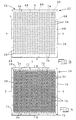
- Each array of pads may comprise twenty five rows of twenty five pads each, as shown in Figure 1.
- the pads may be on centers of 0.060 inches (0.1524cm), 0.075 inches (0.1905cm) or 0.100 inches (0.254cm) for example. These high contact densities are achievable by virtue of arrangement and construction of the connector 20 as described above.
- the plates 22 and 24 can each conveniently be molded in one piece.
Landscapes
- Engineering & Computer Science (AREA)
- Microelectronics & Electronic Packaging (AREA)
- Coupling Device And Connection With Printed Circuit (AREA)
- Connecting Device With Holders (AREA)
Applications Claiming Priority (2)
| Application Number | Priority Date | Filing Date | Title |
|---|---|---|---|
| US314346 | 1989-02-22 | ||
| US07/314,346 US4927369A (en) | 1989-02-22 | 1989-02-22 | Electrical connector for high density usage |
Publications (2)
| Publication Number | Publication Date |
|---|---|
| EP0384656A1 true EP0384656A1 (fr) | 1990-08-29 |
| EP0384656B1 EP0384656B1 (fr) | 1994-02-02 |
Family
ID=23219593
Family Applications (1)
| Application Number | Title | Priority Date | Filing Date |
|---|---|---|---|
| EP90301670A Expired - Lifetime EP0384656B1 (fr) | 1989-02-22 | 1990-02-15 | Connecteur électrique pour utilisation à forte densité |
Country Status (7)
| Country | Link |
|---|---|
| US (1) | US4927369A (fr) |
| EP (1) | EP0384656B1 (fr) |
| JP (1) | JP2819179B2 (fr) |
| KR (1) | KR950004374B1 (fr) |
| DE (1) | DE69006373T2 (fr) |
| DK (1) | DK0384656T3 (fr) |
| IE (1) | IE64482B1 (fr) |
Cited By (3)
| Publication number | Priority date | Publication date | Assignee | Title |
|---|---|---|---|---|
| EP0867980A3 (fr) * | 1997-02-12 | 2001-02-07 | Hirose Electric Co., Ltd. | Connecteur électrique intermédiaire |
| EP1087467A3 (fr) * | 1999-09-24 | 2003-01-15 | Gunsei Kimoto | Contact et assemblage de contacts utilisant celui-ci |
| WO2004095901A1 (fr) * | 2003-03-31 | 2004-11-04 | Intel Corporation | Contact en forme de peigne pour support de boitier lga permettant une distribution d'energie amelioree |
Families Citing this family (102)
| Publication number | Priority date | Publication date | Assignee | Title |
|---|---|---|---|---|
| US4995816A (en) * | 1989-09-29 | 1991-02-26 | Amp Incorporated | Pivotal electrical contact |
| US5015191A (en) * | 1990-03-05 | 1991-05-14 | Amp Incorporated | Flat IC chip connector |
| US5007842A (en) * | 1990-10-11 | 1991-04-16 | Amp Incorporated | Flexible area array connector |
| FR2669149B1 (fr) * | 1990-11-12 | 1994-09-02 | Souriau & Cie | Connecteur intermediaire entre carte de circuit imprime et substrat a circuits electroniques actifs. |
| US5092783A (en) * | 1991-05-16 | 1992-03-03 | Motorola, Inc. | RF interconnect |
| US5167512A (en) * | 1991-07-05 | 1992-12-01 | Walkup William B | Multi-chip module connector element and system |
| US5181852A (en) * | 1991-12-16 | 1993-01-26 | Molex Incorporated | Programmable input-output electrical connector |
| US5230632A (en) * | 1991-12-19 | 1993-07-27 | International Business Machines Corporation | Dual element electrical contact and connector assembly utilizing same |
| JP2658703B2 (ja) * | 1991-12-27 | 1997-09-30 | 日本電気株式会社 | Icソケット |
| US5479320A (en) * | 1991-12-31 | 1995-12-26 | Compaq Computer Corporation | Board-to-board connector including an insulative spacer having a conducting surface and U-shaped contacts |
| US5205738A (en) * | 1992-04-03 | 1993-04-27 | International Business Machines Corporation | High density connector system |
| US5190473A (en) * | 1992-05-18 | 1993-03-02 | Amp Incorporated | Microcoaxial cable connector |
| US5297967A (en) * | 1992-10-13 | 1994-03-29 | International Business Machines Corporation | Electrical interconnector with helical contacting portion and assembly using same |
| US5310352A (en) * | 1992-12-24 | 1994-05-10 | The Whitaker Corporation | Substrate interfacing electrical connector system |
| US5308252A (en) * | 1992-12-24 | 1994-05-03 | The Whitaker Corporation | Interposer connector and contact element therefore |
| US5417578A (en) * | 1992-12-24 | 1995-05-23 | The Whitaker Corporation | Printed wiring boards having low signal-to-ground ratios |
| US5358411A (en) * | 1993-08-09 | 1994-10-25 | The Whitaker Corporation | Duplex plated epsilon compliant beam contact and interposer |
| US5767443A (en) * | 1993-07-10 | 1998-06-16 | Micron Technology, Inc. | Multi-die encapsulation device |
| US5378160A (en) * | 1993-10-01 | 1995-01-03 | Bourns, Inc. | Compliant stacking connector for printed circuit boards |
| US5593927A (en) * | 1993-10-14 | 1997-01-14 | Micron Technology, Inc. | Method for packaging semiconductor dice |
| US5395252A (en) * | 1993-10-27 | 1995-03-07 | Burndy Corporation | Area and edge array electrical connectors |
| US5462440A (en) * | 1994-03-11 | 1995-10-31 | Rothenberger; Richard E. | Micro-power connector |
| EP0771462A4 (fr) * | 1994-07-15 | 1997-10-22 | Berg Tech Inc | Connecteur a bras de compression long, avec une embase en saillie |
| GB9513540D0 (en) * | 1995-07-04 | 1995-09-06 | Elco Europ Ltd | Electrical connectors |
| US5653598A (en) * | 1995-08-31 | 1997-08-05 | The Whitaker Corporation | Electrical contact with reduced self-inductance |
| US5573435A (en) * | 1995-08-31 | 1996-11-12 | The Whitaker Corporation | Tandem loop contact for an electrical connector |
| GB9519204D0 (en) * | 1995-09-20 | 1995-11-22 | Amp Gmbh | Electrical installataion bus connector |
| US5691041A (en) * | 1995-09-29 | 1997-11-25 | International Business Machines Corporation | Socket for semi-permanently connecting a solder ball grid array device using a dendrite interposer |
| DE59710871D1 (de) * | 1996-02-12 | 2003-11-27 | Tyco Electronics Logistics Ag | Leiterplattenverbinder |
| DE19647229C1 (de) * | 1996-11-15 | 1998-02-12 | Telefunken Microelectron | Vorrichtung zum Verbinden von zwei plattenförmigen, elektrotechnische Komponenten tragenden Trägern |
| US6409521B1 (en) * | 1997-05-06 | 2002-06-25 | Gryphics, Inc. | Multi-mode compliant connector and replaceable chip module utilizing the same |
| US5913700A (en) * | 1997-07-14 | 1999-06-22 | The Whitaker Corporation | Card edge connector having low inductance contact system |
| US6200141B1 (en) * | 1997-08-19 | 2001-03-13 | Aries Electronics, Inc. | Land grid array connector |
| FR2768896B1 (fr) * | 1997-09-23 | 1999-11-19 | Matra Marconi Space France | Intercalaire pour boitier micro-electronique et procede de fabrication d'un tel intercalaire |
| US6217342B1 (en) | 1997-10-30 | 2001-04-17 | Intercon Systems, Inc. | Interposer assembly |
| US6315576B1 (en) | 1997-10-30 | 2001-11-13 | Intercon Systems, Inc. | Interposer assembly |
| US6290507B1 (en) | 1997-10-30 | 2001-09-18 | Intercon Systems, Inc. | Interposer assembly |
| JP3256780B2 (ja) * | 1998-02-10 | 2002-02-12 | 日本航空電子工業株式会社 | コネクタ |
| JPH11329648A (ja) * | 1998-05-19 | 1999-11-30 | Molex Inc | Icデバイスソケット |
| US6077089A (en) * | 1999-01-19 | 2000-06-20 | Avx Corporation | Low profile electrical connector |
| US6273731B1 (en) | 1999-01-19 | 2001-08-14 | Avx Corporation | Low profile electrical connector |
| JP2003536203A (ja) | 1999-02-02 | 2003-12-02 | グリフィクス インコーポレーティッド | プリント回路基板及び電気装置のための低挿入力又はゼロ挿入力のコネクタ |
| US6220869B1 (en) * | 1999-05-20 | 2001-04-24 | Airborn, Inc. | Area array connector |
| US6830460B1 (en) * | 1999-08-02 | 2004-12-14 | Gryphics, Inc. | Controlled compliance fine pitch interconnect |
| US6146151A (en) * | 1999-08-18 | 2000-11-14 | Hon Hai Precision Ind. Co., Ltd. | Method for forming an electrical connector and an electrical connector obtained by the method |
| US6358061B1 (en) | 1999-11-09 | 2002-03-19 | Molex Incorporated | High-speed connector with shorting capability |
| US6434817B1 (en) | 1999-12-03 | 2002-08-20 | Delphi Technologies, Inc. | Method for joining an integrated circuit |
| AU2001232772A1 (en) * | 2000-01-20 | 2001-07-31 | Gryphics, Inc. | Flexible compliant interconnect assembly |
| US6957963B2 (en) * | 2000-01-20 | 2005-10-25 | Gryphics, Inc. | Compliant interconnect assembly |
| US6774315B1 (en) * | 2000-05-24 | 2004-08-10 | International Business Machines Corporation | Floating interposer |
| JP2002093541A (ja) * | 2000-09-19 | 2002-03-29 | Miyazaki Oki Electric Co Ltd | Icソケット |
| US6425768B1 (en) | 2000-11-17 | 2002-07-30 | Intercon Systems, Inc. | Clamp connector assembly |
| TW540858U (en) | 2002-08-28 | 2003-07-01 | Hon Hai Prec Ind Co Ltd | Electrical contact |
| DE10300532B4 (de) * | 2003-01-09 | 2010-11-11 | Qimonda Ag | System mit mindestens einer Test-Sockel-Vorrichtung zum Testen von Halbleiter-Bauelementen |
| US7121838B2 (en) * | 2003-04-09 | 2006-10-17 | Intel Corporation | Electronic assembly having angled spring portions |
| US6814586B1 (en) * | 2003-05-01 | 2004-11-09 | Ted Ju | Electric connector |
| TW570354U (en) * | 2003-05-27 | 2004-01-01 | Molex Taiwan Ltd | Electrical connector and its terminal structure |
| US20050173098A1 (en) * | 2003-06-10 | 2005-08-11 | Connors Matthew J. | Three dimensional vapor chamber |
| US20050139995A1 (en) * | 2003-06-10 | 2005-06-30 | David Sarraf | CTE-matched heat pipe |
| US7455556B2 (en) * | 2003-06-11 | 2008-11-25 | Cinch Connectors, Inc. | Electrical contact |
| US6921270B2 (en) | 2003-06-11 | 2005-07-26 | Cinch Connectors, Inc. | Electrical connector |
| US7625216B2 (en) * | 2003-06-11 | 2009-12-01 | Cinch Connectors, Inc. | Electrical connector |
| WO2005008838A1 (fr) * | 2003-07-07 | 2005-01-27 | Gryphics, Inc. | Connecteur a force d'insertion nulle ferme normalement |
| US6994565B2 (en) * | 2003-07-14 | 2006-02-07 | Fci Americas Technology, Inc. | Electrical contact assembly with insulative carrier, stapled contact attachment and fusible element |
| US6945788B2 (en) * | 2003-07-31 | 2005-09-20 | Tyco Electronics Corporation | Metal contact LGA socket |
| US7186119B2 (en) * | 2003-10-17 | 2007-03-06 | Integrated System Technologies, Llc | Interconnection device |
| TWM259337U (en) * | 2003-11-21 | 2005-03-11 | Hon Hai Prec Ind Co Ltd | Electrical connector |
| DE10359648B4 (de) * | 2003-12-18 | 2013-05-16 | Qimonda Ag | Sockel-Einrichtung zur Verwendung beim Test von Halbleiter-Bauelementen, sowie Vorrichtung und Verfahren zum Beladen einer Sockel-Einrichtung mit einem entsprechenden Halbleiter-Bauelement |
| US20050155010A1 (en) * | 2004-01-08 | 2005-07-14 | George M. G. | Method, system and memory for replacing a module |
| TWM256608U (en) * | 2004-02-06 | 2005-02-01 | Hon Hai Prec Ind Co Ltd | Socket connector |
| US7059869B2 (en) * | 2004-02-27 | 2006-06-13 | Tyco Electronics Corporation | Metal contact LGA socket |
| WO2005119849A1 (fr) * | 2004-05-28 | 2005-12-15 | Molex Incorporated | Contact par anneau de frottage flexible |
| TWM266621U (en) * | 2004-08-02 | 2005-06-01 | Hon Hai Prec Ind Co Ltd | Land grid array electrical connector |
| US20060079102A1 (en) * | 2004-10-13 | 2006-04-13 | The Ludlow Company Lp | Cable terminal with flexible contacts |
| US7364477B2 (en) * | 2004-11-12 | 2008-04-29 | Sony Ericsson Mobile Communications Ab | Low profile circuit board connector |
| JP4471941B2 (ja) * | 2005-03-10 | 2010-06-02 | 山一電機株式会社 | 半導体装置用ソケット |
| CN2779655Y (zh) * | 2005-03-29 | 2006-05-10 | 番禺得意精密电子工业有限公司 | 电连接器 |
| JP4973988B2 (ja) * | 2006-06-12 | 2012-07-11 | 山一電機株式会社 | コンタクト及びこれを用いたicソケット |
| US7338294B2 (en) * | 2006-06-28 | 2008-03-04 | Hon Hai Precision Ind. Co., Ltd. | Pressure contact connector |
| DE102007006212B4 (de) * | 2007-02-08 | 2012-09-13 | Semikron Elektronik Gmbh & Co. Kg | Leistungshalbleitermodul mit Kontaktfedern |
| US7534133B2 (en) * | 2007-03-05 | 2009-05-19 | Tyco Electronics Corporation | Electrical connector assembly with alignment pin |
| US20080293308A1 (en) * | 2007-05-24 | 2008-11-27 | Tribotek, Inc. | Pivoting wafer connector |
| JP2009036679A (ja) * | 2007-08-02 | 2009-02-19 | Yamaichi Electronics Co Ltd | 半導体装置用ソケット |
| JP4495200B2 (ja) * | 2007-09-28 | 2010-06-30 | 山一電機株式会社 | 半導体装置用ソケット |
| JP5334997B2 (ja) * | 2008-01-17 | 2013-11-06 | アンフェノル・コーポレーション | インターポーザ・アセンブリ及び方法 |
| US7806699B2 (en) * | 2008-01-31 | 2010-10-05 | Methode Electornics, Inc. | Wound coil compression connector |
| US7794235B2 (en) | 2008-01-31 | 2010-09-14 | Methode Electronics, Inc. | Continuous wireform connector |
| US7806737B2 (en) * | 2008-02-04 | 2010-10-05 | Methode Electronics, Inc. | Stamped beam connector |
| JP2010118275A (ja) * | 2008-11-13 | 2010-05-27 | Yamaichi Electronics Co Ltd | 半導体装置用ソケット |
| JP5401101B2 (ja) * | 2009-01-08 | 2014-01-29 | 富士通コンポーネント株式会社 | コンタクト部材、及び該コンタクト部材を含むコネクタ |
| US8758026B2 (en) | 2012-02-06 | 2014-06-24 | Touchsensor Technologies, Llc | System for connecting a first substrate to a second substrate |
| US20180241143A1 (en) * | 2014-11-28 | 2018-08-23 | Avic Jonhon Optronic Technology Co., Ltd | M-like elastic contact spring and terminated adaptor connector |
| CN107492728A (zh) * | 2017-01-12 | 2017-12-19 | 番禺得意精密电子工业有限公司 | 电连接器 |
| CN107394448B (zh) * | 2017-07-14 | 2019-01-22 | 番禺得意精密电子工业有限公司 | 电连接器及电子装置 |
| CN109560406B (zh) * | 2018-03-14 | 2020-06-30 | 番禺得意精密电子工业有限公司 | 电连接器 |
| CN111064031B (zh) | 2019-11-25 | 2021-05-25 | 番禺得意精密电子工业有限公司 | 电连接器及其制造方法 |
| CN113783066B (zh) * | 2021-08-09 | 2023-10-24 | 番禺得意精密电子工业有限公司 | 电连接器及其制造方法 |
| CN113948897B (zh) * | 2021-09-10 | 2023-07-21 | 番禺得意精密电子工业有限公司 | 电连接器 |
| US20240006784A1 (en) * | 2022-06-30 | 2024-01-04 | Amphenol Corporation | Interposer with contact retention with heat stake |
| US20240106147A1 (en) * | 2022-09-26 | 2024-03-28 | Fuding Precision Components (Shenzhen) Co., Ltd. | Electrical connector with improved terminals |
| US20240154340A1 (en) * | 2022-11-03 | 2024-05-09 | Fuding Precision Components (Shenzhen) Co., Ltd. | Electrical connector with improved grounding terminals |
| CN116667013A (zh) * | 2023-05-30 | 2023-08-29 | 立讯精密工业股份有限公司 | 板对板连接器 |
Citations (2)
| Publication number | Priority date | Publication date | Assignee | Title |
|---|---|---|---|---|
| US4505529A (en) * | 1983-11-01 | 1985-03-19 | Amp Incorporated | Electrical connector for use between circuit boards |
| EP0255244A1 (fr) * | 1986-07-31 | 1988-02-03 | Amp Incorporated | Connecteur comportant des modules de contact pour un substrat tel qu'un porteur de microplaquettes pour circuits intégrés |
Family Cites Families (8)
| Publication number | Priority date | Publication date | Assignee | Title |
|---|---|---|---|---|
| NL158033B (nl) * | 1974-02-27 | 1978-09-15 | Amp Inc | Verbetering van een elektrisch verbindingsorgaan voor het losneembaar verbinden van twee vaste contactdragers en werkwijze voor het vervaardigen van zulk een elektrisch verbindingsorgaan. |
| JPS52109587U (fr) * | 1976-02-18 | 1977-08-20 | ||
| JPS5412621A (en) * | 1977-06-30 | 1979-01-30 | Fujitsu Ltd | Picture signal process system |
| US4482937A (en) * | 1982-09-30 | 1984-11-13 | Control Data Corporation | Board to board interconnect structure |
| US4513353A (en) * | 1982-12-27 | 1985-04-23 | Amp Incorporated | Connection of leadless integrated circuit package to a circuit board |
| US4511197A (en) * | 1983-08-01 | 1985-04-16 | Amp Incorporated | High density contact assembly |
| US4647124A (en) * | 1985-10-16 | 1987-03-03 | Amp Incorporated | Electrical connector for interconnecting arrays of conductive areas |
| JPS62217692A (ja) * | 1986-01-10 | 1987-09-25 | テイア−ルダブリユ− インコ−ポレ−テツド | 両面印刷回路基板モジユ−ル |
-
1989
- 1989-02-22 US US07/314,346 patent/US4927369A/en not_active Expired - Lifetime
-
1990
- 1990-02-15 EP EP90301670A patent/EP0384656B1/fr not_active Expired - Lifetime
- 1990-02-15 DE DE69006373T patent/DE69006373T2/de not_active Expired - Fee Related
- 1990-02-15 DK DK90301670.7T patent/DK0384656T3/da active
- 1990-02-16 IE IE57490A patent/IE64482B1/en not_active IP Right Cessation
- 1990-02-20 JP JP2037550A patent/JP2819179B2/ja not_active Expired - Lifetime
- 1990-02-21 KR KR1019900002106A patent/KR950004374B1/ko not_active Expired - Fee Related
Patent Citations (2)
| Publication number | Priority date | Publication date | Assignee | Title |
|---|---|---|---|---|
| US4505529A (en) * | 1983-11-01 | 1985-03-19 | Amp Incorporated | Electrical connector for use between circuit boards |
| EP0255244A1 (fr) * | 1986-07-31 | 1988-02-03 | Amp Incorporated | Connecteur comportant des modules de contact pour un substrat tel qu'un porteur de microplaquettes pour circuits intégrés |
Non-Patent Citations (2)
| Title |
|---|
| IBM TECHNICAL DISCLOSURE BULLETIN. vol. 24, no. 12, May 1982, NEW YORK US pages 6366 - 6369; R.J.REDMOND and T.R.TOUW: "Socket assembly for pinless array integrated circuit package." * |
| IBM TECHNICAL DISCLOSURE BULLETIN. vol. 6, no. 10, March 1964, NEW YORK US pages 5 - 6; H.C.SCHICK: "Plated through hole contact." * |
Cited By (4)
| Publication number | Priority date | Publication date | Assignee | Title |
|---|---|---|---|---|
| EP0867980A3 (fr) * | 1997-02-12 | 2001-02-07 | Hirose Electric Co., Ltd. | Connecteur électrique intermédiaire |
| EP1087467A3 (fr) * | 1999-09-24 | 2003-01-15 | Gunsei Kimoto | Contact et assemblage de contacts utilisant celui-ci |
| WO2004095901A1 (fr) * | 2003-03-31 | 2004-11-04 | Intel Corporation | Contact en forme de peigne pour support de boitier lga permettant une distribution d'energie amelioree |
| CN100551216C (zh) * | 2003-03-31 | 2009-10-14 | 英特尔公司 | 用于改进电力输送的接点栅格阵列的设备、系统和方法 |
Also Published As
| Publication number | Publication date |
|---|---|
| DE69006373T2 (de) | 1994-09-01 |
| DE69006373D1 (de) | 1994-03-17 |
| KR900013676A (ko) | 1990-09-06 |
| JPH02247995A (ja) | 1990-10-03 |
| JP2819179B2 (ja) | 1998-10-30 |
| IE900574L (en) | 1990-08-22 |
| KR950004374B1 (ko) | 1995-04-28 |
| US4927369A (en) | 1990-05-22 |
| IE64482B1 (en) | 1995-08-09 |
| DK0384656T3 (da) | 1994-03-07 |
| EP0384656B1 (fr) | 1994-02-02 |
Similar Documents
| Publication | Publication Date | Title |
|---|---|---|
| EP0384656B1 (fr) | Connecteur électrique pour utilisation à forte densité | |
| US5669774A (en) | Ball grid array socket | |
| EP0416322B1 (fr) | Borne de contact dans un support pour platine de circuits | |
| EP0384580B1 (fr) | Contact HDI pour montage en surface | |
| US6929483B2 (en) | Electrical contact having contact portion with enhanced resiliency | |
| US6183301B1 (en) | Surface mount connector with integrated PCB assembly | |
| US5055054A (en) | High density connector | |
| US6729890B2 (en) | Reduced-size board-to-board connector | |
| US4018494A (en) | Interconnection for electrically connecting two vertically stacked electronic packages | |
| EP0232103B1 (fr) | Agencement de broche et alvéole de prise de courant électrique pour connecteurs à fiches et douilles | |
| US5634801A (en) | Electrical interconnect contact system | |
| EP0340730B1 (fr) | Dispositif à contacts multiples pour recevoir le coté de contact d'une plaquette mince à circuits imprimés, et élément de contact flexible à cet effet | |
| US4973270A (en) | Circuit panel socket with cloverleaf contact | |
| US6561819B1 (en) | Terminals of socket connector | |
| JPH0785426B2 (ja) | コネクター,回路板の接点要素およびその保持部 | |
| US6089883A (en) | Board-to-board connector assembly | |
| EP1128477A2 (fr) | Connecteur électrique avec contacts à compression | |
| US6450824B1 (en) | Connector including movable cover | |
| US5009606A (en) | Separable electrical connector | |
| US20020115324A1 (en) | Ball attached zero insertion force socket | |
| EP0400378B1 (fr) | Socle de panneau de circuit imprimé à contact en forme de trèfle | |
| JP2002367736A (ja) | 端子ブロック及びケーブルコネクタ | |
| US6575791B1 (en) | Electrical connector providing reliable electrical interconnection with mated devices | |
| JP3303222B2 (ja) | Zifコネクタ | |
| HK1000401B (en) | Improved electrical plug pin and receptacle arrangement for plug and socket connectors |
Legal Events
| Date | Code | Title | Description |
|---|---|---|---|
| PUAI | Public reference made under article 153(3) epc to a published international application that has entered the european phase |
Free format text: ORIGINAL CODE: 0009012 |
|
| AK | Designated contracting states |
Kind code of ref document: A1 Designated state(s): DE DK FR GB IT NL SE |
|
| 17P | Request for examination filed |
Effective date: 19900928 |
|
| RAP1 | Party data changed (applicant data changed or rights of an application transferred) |
Owner name: THE WHITAKER CORPORATION |
|
| 17Q | First examination report despatched |
Effective date: 19930315 |
|
| GRAA | (expected) grant |
Free format text: ORIGINAL CODE: 0009210 |
|
| AK | Designated contracting states |
Kind code of ref document: B1 Designated state(s): DE DK FR GB IT NL SE |
|
| REG | Reference to a national code |
Ref country code: DK Ref legal event code: T3 |
|
| REF | Corresponds to: |
Ref document number: 69006373 Country of ref document: DE Date of ref document: 19940317 |
|
| ET | Fr: translation filed | ||
| ITF | It: translation for a ep patent filed | ||
| PLBE | No opposition filed within time limit |
Free format text: ORIGINAL CODE: 0009261 |
|
| STAA | Information on the status of an ep patent application or granted ep patent |
Free format text: STATUS: NO OPPOSITION FILED WITHIN TIME LIMIT |
|
| 26N | No opposition filed | ||
| EAL | Se: european patent in force in sweden |
Ref document number: 90301670.7 |
|
| PGFP | Annual fee paid to national office [announced via postgrant information from national office to epo] |
Ref country code: DK Payment date: 19971229 Year of fee payment: 9 |
|
| PGFP | Annual fee paid to national office [announced via postgrant information from national office to epo] |
Ref country code: NL Payment date: 19971231 Year of fee payment: 9 |
|
| PGFP | Annual fee paid to national office [announced via postgrant information from national office to epo] |
Ref country code: GB Payment date: 19980108 Year of fee payment: 9 |
|
| PGFP | Annual fee paid to national office [announced via postgrant information from national office to epo] |
Ref country code: SE Payment date: 19980205 Year of fee payment: 9 |
|
| PGFP | Annual fee paid to national office [announced via postgrant information from national office to epo] |
Ref country code: FR Payment date: 19980209 Year of fee payment: 9 |
|
| PGFP | Annual fee paid to national office [announced via postgrant information from national office to epo] |
Ref country code: DE Payment date: 19980227 Year of fee payment: 9 |
|
| PG25 | Lapsed in a contracting state [announced via postgrant information from national office to epo] |
Ref country code: GB Free format text: LAPSE BECAUSE OF NON-PAYMENT OF DUE FEES Effective date: 19990215 |
|
| PG25 | Lapsed in a contracting state [announced via postgrant information from national office to epo] |
Ref country code: SE Free format text: LAPSE BECAUSE OF NON-PAYMENT OF DUE FEES Effective date: 19990216 |
|
| PG25 | Lapsed in a contracting state [announced via postgrant information from national office to epo] |
Ref country code: DK Free format text: LAPSE BECAUSE OF NON-PAYMENT OF DUE FEES Effective date: 19990301 |
|
| PG25 | Lapsed in a contracting state [announced via postgrant information from national office to epo] |
Ref country code: NL Free format text: LAPSE BECAUSE OF NON-PAYMENT OF DUE FEES Effective date: 19990901 |
|
| GBPC | Gb: european patent ceased through non-payment of renewal fee |
Effective date: 19990215 |
|
| PG25 | Lapsed in a contracting state [announced via postgrant information from national office to epo] |
Ref country code: FR Free format text: LAPSE BECAUSE OF NON-PAYMENT OF DUE FEES Effective date: 19991029 |
|
| EUG | Se: european patent has lapsed |
Ref document number: 90301670.7 |
|
| PG25 | Lapsed in a contracting state [announced via postgrant information from national office to epo] |
Ref country code: DE Free format text: LAPSE BECAUSE OF NON-PAYMENT OF DUE FEES Effective date: 19991201 |
|
| REG | Reference to a national code |
Ref country code: FR Ref legal event code: ST |
|
| REG | Reference to a national code |
Ref country code: DK Ref legal event code: EBP |
|
| PG25 | Lapsed in a contracting state [announced via postgrant information from national office to epo] |
Ref country code: IT Free format text: LAPSE BECAUSE OF NON-PAYMENT OF DUE FEES;WARNING: LAPSES OF ITALIAN PATENTS WITH EFFECTIVE DATE BEFORE 2007 MAY HAVE OCCURRED AT ANY TIME BEFORE 2007. THE CORRECT EFFECTIVE DATE MAY BE DIFFERENT FROM THE ONE RECORDED. Effective date: 20050215 |