EP0384849A2 - Système semi-conducteur d'émission de lumière - Google Patents
Système semi-conducteur d'émission de lumière Download PDFInfo
- Publication number
- EP0384849A2 EP0384849A2 EP19900400509 EP90400509A EP0384849A2 EP 0384849 A2 EP0384849 A2 EP 0384849A2 EP 19900400509 EP19900400509 EP 19900400509 EP 90400509 A EP90400509 A EP 90400509A EP 0384849 A2 EP0384849 A2 EP 0384849A2
- Authority
- EP
- European Patent Office
- Prior art keywords
- light emitting
- microlens
- semiconductor
- plane
- lens
- Prior art date
- Legal status (The legal status is an assumption and is not a legal conclusion. Google has not performed a legal analysis and makes no representation as to the accuracy of the status listed.)
- Granted
Links
Images








Classifications
-
- H—ELECTRICITY
- H01—ELECTRIC ELEMENTS
- H01S—DEVICES USING THE PROCESS OF LIGHT AMPLIFICATION BY STIMULATED EMISSION OF RADIATION [LASER] TO AMPLIFY OR GENERATE LIGHT; DEVICES USING STIMULATED EMISSION OF ELECTROMAGNETIC RADIATION IN WAVE RANGES OTHER THAN OPTICAL
- H01S5/00—Semiconductor lasers
- H01S5/02—Structural details or components not essential to laser action
- H01S5/026—Monolithically integrated components, e.g. waveguides, monitoring photo-detectors, drivers
-
- G—PHYSICS
- G02—OPTICS
- G02B—OPTICAL ELEMENTS, SYSTEMS OR APPARATUS
- G02B6/00—Light guides; Structural details of arrangements comprising light guides and other optical elements, e.g. couplings
- G02B6/24—Coupling light guides
- G02B6/42—Coupling light guides with opto-electronic elements
-
- G—PHYSICS
- G02—OPTICS
- G02B—OPTICAL ELEMENTS, SYSTEMS OR APPARATUS
- G02B6/00—Light guides; Structural details of arrangements comprising light guides and other optical elements, e.g. couplings
- G02B6/24—Coupling light guides
- G02B6/42—Coupling light guides with opto-electronic elements
- G02B6/4201—Packages, e.g. shape, construction, internal or external details
- G02B6/4204—Packages, e.g. shape, construction, internal or external details the coupling comprising intermediate optical elements, e.g. lenses, holograms
-
- H—ELECTRICITY
- H10—SEMICONDUCTOR DEVICES; ELECTRIC SOLID-STATE DEVICES NOT OTHERWISE PROVIDED FOR
- H10H—INORGANIC LIGHT-EMITTING SEMICONDUCTOR DEVICES HAVING POTENTIAL BARRIERS
- H10H20/00—Individual inorganic light-emitting semiconductor devices having potential barriers, e.g. light-emitting diodes [LED]
- H10H20/80—Constructional details
- H10H20/85—Packages
- H10H20/855—Optical field-shaping means, e.g. lenses
-
- H—ELECTRICITY
- H01—ELECTRIC ELEMENTS
- H01S—DEVICES USING THE PROCESS OF LIGHT AMPLIFICATION BY STIMULATED EMISSION OF RADIATION [LASER] TO AMPLIFY OR GENERATE LIGHT; DEVICES USING STIMULATED EMISSION OF ELECTROMAGNETIC RADIATION IN WAVE RANGES OTHER THAN OPTICAL
- H01S3/00—Lasers, i.e. devices using stimulated emission of electromagnetic radiation in the infrared, visible or ultraviolet wave range
- H01S3/005—Optical devices external to the laser cavity, specially adapted for lasers, e.g. for homogenisation of the beam or for manipulating laser pulses, e.g. pulse shaping
-
- H—ELECTRICITY
- H01—ELECTRIC ELEMENTS
- H01S—DEVICES USING THE PROCESS OF LIGHT AMPLIFICATION BY STIMULATED EMISSION OF RADIATION [LASER] TO AMPLIFY OR GENERATE LIGHT; DEVICES USING STIMULATED EMISSION OF ELECTROMAGNETIC RADIATION IN WAVE RANGES OTHER THAN OPTICAL
- H01S5/00—Semiconductor lasers
- H01S5/005—Optical components external to the laser cavity, specially adapted therefor, e.g. for homogenisation or merging of the beams or for manipulating laser pulses, e.g. pulse shaping
-
- H—ELECTRICITY
- H01—ELECTRIC ELEMENTS
- H01S—DEVICES USING THE PROCESS OF LIGHT AMPLIFICATION BY STIMULATED EMISSION OF RADIATION [LASER] TO AMPLIFY OR GENERATE LIGHT; DEVICES USING STIMULATED EMISSION OF ELECTROMAGNETIC RADIATION IN WAVE RANGES OTHER THAN OPTICAL
- H01S5/00—Semiconductor lasers
- H01S5/40—Arrangement of two or more semiconductor lasers, not provided for in groups H01S5/02 - H01S5/30
- H01S5/4025—Array arrangements, e.g. constituted by discrete laser diodes or laser bar
-
- H—ELECTRICITY
- H01—ELECTRIC ELEMENTS
- H01S—DEVICES USING THE PROCESS OF LIGHT AMPLIFICATION BY STIMULATED EMISSION OF RADIATION [LASER] TO AMPLIFY OR GENERATE LIGHT; DEVICES USING STIMULATED EMISSION OF ELECTROMAGNETIC RADIATION IN WAVE RANGES OTHER THAN OPTICAL
- H01S5/00—Semiconductor lasers
- H01S5/40—Arrangement of two or more semiconductor lasers, not provided for in groups H01S5/02 - H01S5/30
- H01S5/4025—Array arrangements, e.g. constituted by discrete laser diodes or laser bar
- H01S5/4031—Edge-emitting structures
Definitions
- a microlens deposited on a semiconductor substrate is small in size as compared with a prior separated microlens. Therefore, a semiconductor system including a laser and a lens is small in size. And, when a plurality of lasers are mounted in a matrix manner, each beam may be focused by using the specific lens for each beam. In a prior art, a lens is common to a plurality of beams, and therefore, the focusing for each beam is impossible.
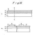
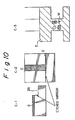
- Fig.10(B)-3 is a plane view after the stripe step
- Fig.10(B)-2 is the cross section of Fig.10(B)-3.
- Fig.2 shows the structure of another embodiment of a semiconductor light emitting system according to the present invention.
- the same numerals in Fig.2 show the same members as those in Fig.1.
- the microlens 202 has all the effects of those of the microlens 2 in Fig.1, except that the microlens 202 is a concave lens. It is easy to align an optical axis of a microlens 202 with that of a light emitting element 1 in producing process.
- the microlens 202 is small in size and light in weight, as the microlens 2 in Fig.1. Also, since the size of the microlens is larger than 50 ⁇ m in each direction, no diffraction of light beam occurs.
- Fig.3 shows still another embodiment of a semiconductor light emitting system according to the present invention.
- the same numerals as those in Fig.3 show the same members as those of Fig.1.
- the feature of the embodiment of Fig.3 is the presence of a microlens 302, instead of the microlens 2 in Fig.1.
- the microlens 302 in Fig.3 is composed of a transparent layer 330, which is in flat shap having a flat input plane 31 perpendicular to the main plane 11a of the semiconductor substrate 11, and a convex output plane perpendicular to said main plane 11a.
Landscapes
- Physics & Mathematics (AREA)
- General Physics & Mathematics (AREA)
- Optics & Photonics (AREA)
- Condensed Matter Physics & Semiconductors (AREA)
- Electromagnetism (AREA)
- Semiconductor Lasers (AREA)
- Led Device Packages (AREA)
Applications Claiming Priority (2)
| Application Number | Priority Date | Filing Date | Title |
|---|---|---|---|
| JP44382/89 | 1989-02-24 | ||
| JP1044382A JPH0744313B2 (ja) | 1989-02-24 | 1989-02-24 | 半導体レーザ装置 |
Publications (3)
| Publication Number | Publication Date |
|---|---|
| EP0384849A2 true EP0384849A2 (fr) | 1990-08-29 |
| EP0384849A3 EP0384849A3 (fr) | 1992-10-21 |
| EP0384849B1 EP0384849B1 (fr) | 1994-10-05 |
Family
ID=12689955
Family Applications (1)
| Application Number | Title | Priority Date | Filing Date |
|---|---|---|---|
| EP90400509A Expired - Lifetime EP0384849B1 (fr) | 1989-02-24 | 1990-02-23 | Système semi-conducteur d'émission de lumière |
Country Status (4)
| Country | Link |
|---|---|
| US (1) | US5084895A (fr) |
| EP (1) | EP0384849B1 (fr) |
| JP (1) | JPH0744313B2 (fr) |
| DE (1) | DE69013032T2 (fr) |
Cited By (4)
| Publication number | Priority date | Publication date | Assignee | Title |
|---|---|---|---|---|
| EP0525433A1 (fr) * | 1991-07-31 | 1993-02-03 | Siemens Aktiengesellschaft | Dispositif pour le couplage d'un signal optique dans une fibre optique |
| US5428227A (en) * | 1993-03-17 | 1995-06-27 | Ricoh Company, Ltd. | Semiconductor light emitting element |
| US6570324B1 (en) | 2000-07-19 | 2003-05-27 | Eastman Kodak Company | Image display device with array of lens-lets |
| WO2003075052A3 (fr) * | 2002-02-28 | 2004-04-01 | Sarnoff Corp | Convertisseur a taille du point integre a base d'alliage de silicium amorphe |
Families Citing this family (19)
| Publication number | Priority date | Publication date | Assignee | Title |
|---|---|---|---|---|
| CA2056272C (fr) * | 1991-06-14 | 2001-10-16 | Patrick Salatto, Jr. | Dispositif de balayage laser a plages combinees |
| US5619488A (en) * | 1991-09-07 | 1997-04-08 | Fuji Xerox Co., Ltd. | Information recording device |
| US5222095A (en) * | 1992-03-30 | 1993-06-22 | Mcdonnell Douglas Corporation | Rib etched lens |
| US5544184A (en) * | 1994-06-10 | 1996-08-06 | Sdl, Inc. | Semiconductor illumination system with expansion matched components |
| KR100393057B1 (ko) * | 2000-10-20 | 2003-07-31 | 삼성전자주식회사 | 마이크로 렌즈 일체형 표면광 레이저 |
| US7139300B2 (en) * | 2003-08-19 | 2006-11-21 | Coherent, Inc. | Wide-stripe single-mode diode-laser |
| JP4225179B2 (ja) * | 2003-10-17 | 2009-02-18 | 株式会社日立製作所 | 光学素子実装用基板およびその製造方法 |
| JP4789423B2 (ja) * | 2004-03-30 | 2011-10-12 | キヤノン株式会社 | 光導波装置 |
| JP4117499B2 (ja) * | 2006-08-02 | 2008-07-16 | セイコーエプソン株式会社 | 面発光型半導体レーザ |
| US10203399B2 (en) | 2013-11-12 | 2019-02-12 | Big Sky Financial Corporation | Methods and apparatus for array based LiDAR systems with reduced interference |
| US9360554B2 (en) | 2014-04-11 | 2016-06-07 | Facet Technology Corp. | Methods and apparatus for object detection and identification in a multiple detector lidar array |
| US10036801B2 (en) | 2015-03-05 | 2018-07-31 | Big Sky Financial Corporation | Methods and apparatus for increased precision and improved range in a multiple detector LiDAR array |
| US9866816B2 (en) | 2016-03-03 | 2018-01-09 | 4D Intellectual Properties, Llc | Methods and apparatus for an active pulsed 4D camera for image acquisition and analysis |
| DE102017123798B4 (de) * | 2017-10-12 | 2022-03-03 | OSRAM Opto Semiconductors Gesellschaft mit beschränkter Haftung | Halbleiterlaser und Herstellungsverfahren für optoelektronische Halbleiterbauteile |
| JP7351185B2 (ja) * | 2019-11-05 | 2023-09-27 | 住友電気工業株式会社 | 量子カスケードレーザ |
| US11176962B1 (en) * | 2020-09-10 | 2021-11-16 | Seagate Technology Llc | Heat-assisted magnetic recording laser with a curved facet |
| US12164147B2 (en) * | 2021-06-25 | 2024-12-10 | Intel Corporation | Device, method and system for optical communication with a waveguide structure and an integrated optical coupler of a photonic integrated circuit chip |
| US12298572B2 (en) | 2021-06-25 | 2025-05-13 | Intel Corporation | Device, method and system for optical communication with a photonic integrated circuit chip and a transverse oriented lens structure |
| US20230194791A1 (en) * | 2021-12-21 | 2023-06-22 | Intel Corporation | Electronic device including a grin lens |
Family Cites Families (11)
| Publication number | Priority date | Publication date | Assignee | Title |
|---|---|---|---|---|
| US3835414A (en) * | 1972-03-24 | 1974-09-10 | Us Air Force | Gallium arsenide array |
| GB1454188A (fr) * | 1973-12-03 | 1976-10-27 | ||
| US4297653A (en) * | 1979-04-30 | 1981-10-27 | Xerox Corporation | Hybrid semiconductor laser/detectors |
| JPS5988885A (ja) * | 1982-11-12 | 1984-05-22 | Agency Of Ind Science & Technol | 集積化光発振器 |
| JPS6235688A (ja) * | 1985-08-09 | 1987-02-16 | Sanyo Electric Co Ltd | 半導体レ−ザ装置 |
| JPS62107304A (ja) * | 1985-11-06 | 1987-05-18 | Mitsubishi Electric Corp | プログラマブルコントロ−ラ |
| JPH0795156B2 (ja) * | 1986-02-14 | 1995-10-11 | オムロン株式会社 | マイクロ・レンズ装置 |
| JPS62213188A (ja) * | 1986-03-14 | 1987-09-19 | Hitachi Ltd | 半導体レ−ザ素子 |
| JPH0546919Y2 (fr) * | 1986-04-22 | 1993-12-09 | ||
| JPS62275332A (ja) * | 1986-05-23 | 1987-11-30 | Nippon Telegr & Teleph Corp <Ntt> | 光ヘツド |
| JP2516953B2 (ja) * | 1987-02-17 | 1996-07-24 | 松下電器産業株式会社 | 半導体レ―ザ装置の製造方法 |
-
1989
- 1989-02-24 JP JP1044382A patent/JPH0744313B2/ja not_active Expired - Lifetime
-
1990
- 1990-02-23 US US07/483,853 patent/US5084895A/en not_active Expired - Lifetime
- 1990-02-23 DE DE69013032T patent/DE69013032T2/de not_active Expired - Fee Related
- 1990-02-23 EP EP90400509A patent/EP0384849B1/fr not_active Expired - Lifetime
Cited By (5)
| Publication number | Priority date | Publication date | Assignee | Title |
|---|---|---|---|---|
| EP0525433A1 (fr) * | 1991-07-31 | 1993-02-03 | Siemens Aktiengesellschaft | Dispositif pour le couplage d'un signal optique dans une fibre optique |
| US5428227A (en) * | 1993-03-17 | 1995-06-27 | Ricoh Company, Ltd. | Semiconductor light emitting element |
| US6570324B1 (en) | 2000-07-19 | 2003-05-27 | Eastman Kodak Company | Image display device with array of lens-lets |
| WO2003075052A3 (fr) * | 2002-02-28 | 2004-04-01 | Sarnoff Corp | Convertisseur a taille du point integre a base d'alliage de silicium amorphe |
| US6888984B2 (en) | 2002-02-28 | 2005-05-03 | Sarnoff Corporation | Amorphous silicon alloy based integrated spot-size converter |
Also Published As
| Publication number | Publication date |
|---|---|
| US5084895A (en) | 1992-01-28 |
| EP0384849B1 (fr) | 1994-10-05 |
| EP0384849A3 (fr) | 1992-10-21 |
| DE69013032D1 (de) | 1994-11-10 |
| DE69013032T2 (de) | 1995-01-26 |
| JPH02222589A (ja) | 1990-09-05 |
| JPH0744313B2 (ja) | 1995-05-15 |
Similar Documents
| Publication | Publication Date | Title |
|---|---|---|
| EP0384849B1 (fr) | Système semi-conducteur d'émission de lumière | |
| US5212707A (en) | Array of diffraction limited lasers and method of aligning same | |
| EP3888204B1 (fr) | Émetteurs verticaux à microlentilles intégrées | |
| US6128134A (en) | Integrated beam shaper and use thereof | |
| US5148322A (en) | Micro aspherical lens and fabricating method therefor and optical device | |
| US5164956A (en) | Multiperiod-grating surface-emitting lasers | |
| US5853626A (en) | Optical module and a fabrication process thereof | |
| DE69429466T2 (de) | Optische Vorrichtung | |
| DE102005031132B4 (de) | Optoelektronisches Modul mit hohem Kopplungswirkungsgrad | |
| US5400311A (en) | Hologram and optical apparatus with hologram | |
| EP0928481A2 (fr) | Appareil a tete optique integree et procedes associes | |
| US5327415A (en) | Integrated light deflector and method of fabrication therefor | |
| EP0499946B1 (fr) | DEL avec réflecteur à facettes multiples pour augmenter l'efficacité de couplage et la tolérance d'ajustage | |
| JPS63191329A (ja) | 集積型光ピックアップ装置 | |
| JP2001028456A (ja) | 半導体発光素子 | |
| US7218804B2 (en) | Method and device for establishing an optical connection between an optoelectronic component and an optical waveguide | |
| US7031572B2 (en) | Optical coupler | |
| US6303402B1 (en) | Method of manufacturing near field light generating device | |
| JP2783806B2 (ja) | 光出力モニタ装置 | |
| US20030063859A1 (en) | Optical module and method of forming the optical module | |
| JP2003121615A (ja) | 光接続モジュールの製造方法 | |
| JPS61127190A (ja) | 半導体装置 | |
| Hillman | How manufacturing errors in binary optics arrays affect far field patterns | |
| JP2003043293A (ja) | 光モジュール及び光モジュールの作製方法 | |
| JPH05215909A (ja) | 光学レンズ |
Legal Events
| Date | Code | Title | Description |
|---|---|---|---|
| PUAI | Public reference made under article 153(3) epc to a published international application that has entered the european phase |
Free format text: ORIGINAL CODE: 0009012 |
|
| AK | Designated contracting states |
Kind code of ref document: A2 Designated state(s): DE FR GB |
|
| RIN1 | Information on inventor provided before grant (corrected) |
Inventor name: SHIMADA, JUNICHI, C/O NTT TOMOMIHARA-DORMITORY Inventor name: SAWADA, RENSHI |
|
| RIN1 | Information on inventor provided before grant (corrected) |
Inventor name: SAWADA, RENSHI Inventor name: SHIMADA, JUNICHI, C/O 5-405, NTT DORMITORY |
|
| PUAL | Search report despatched |
Free format text: ORIGINAL CODE: 0009013 |
|
| AK | Designated contracting states |
Kind code of ref document: A3 Designated state(s): DE FR GB |
|
| RHK1 | Main classification (correction) |
Ipc: H01S 3/19 |
|
| 17P | Request for examination filed |
Effective date: 19921126 |
|
| 17Q | First examination report despatched |
Effective date: 19930511 |
|
| GRAA | (expected) grant |
Free format text: ORIGINAL CODE: 0009210 |
|
| AK | Designated contracting states |
Kind code of ref document: B1 Designated state(s): DE FR GB |
|
| REF | Corresponds to: |
Ref document number: 69013032 Country of ref document: DE Date of ref document: 19941110 |
|
| ET | Fr: translation filed | ||
| PLBE | No opposition filed within time limit |
Free format text: ORIGINAL CODE: 0009261 |
|
| STAA | Information on the status of an ep patent application or granted ep patent |
Free format text: STATUS: NO OPPOSITION FILED WITHIN TIME LIMIT |
|
| 26N | No opposition filed | ||
| REG | Reference to a national code |
Ref country code: FR Ref legal event code: CA |
|
| REG | Reference to a national code |
Ref country code: GB Ref legal event code: IF02 |
|
| PGFP | Annual fee paid to national office [announced via postgrant information from national office to epo] |
Ref country code: DE Payment date: 20080220 Year of fee payment: 19 Ref country code: GB Payment date: 20080220 Year of fee payment: 19 |
|
| PGFP | Annual fee paid to national office [announced via postgrant information from national office to epo] |
Ref country code: FR Payment date: 20080226 Year of fee payment: 19 |
|
| GBPC | Gb: european patent ceased through non-payment of renewal fee |
Effective date: 20090223 |
|
| REG | Reference to a national code |
Ref country code: FR Ref legal event code: ST Effective date: 20091030 |
|
| PG25 | Lapsed in a contracting state [announced via postgrant information from national office to epo] |
Ref country code: DE Free format text: LAPSE BECAUSE OF NON-PAYMENT OF DUE FEES Effective date: 20090901 |
|
| PG25 | Lapsed in a contracting state [announced via postgrant information from national office to epo] |
Ref country code: FR Free format text: LAPSE BECAUSE OF NON-PAYMENT OF DUE FEES Effective date: 20090302 Ref country code: GB Free format text: LAPSE BECAUSE OF NON-PAYMENT OF DUE FEES Effective date: 20090223 |