EP0385019B1 - Elektrischer Verbinder mit vorgespannten Kontakten und Verfahren zu dessen Herstellung - Google Patents
Elektrischer Verbinder mit vorgespannten Kontakten und Verfahren zu dessen Herstellung Download PDFInfo
- Publication number
- EP0385019B1 EP0385019B1 EP89304336A EP89304336A EP0385019B1 EP 0385019 B1 EP0385019 B1 EP 0385019B1 EP 89304336 A EP89304336 A EP 89304336A EP 89304336 A EP89304336 A EP 89304336A EP 0385019 B1 EP0385019 B1 EP 0385019B1
- Authority
- EP
- European Patent Office
- Prior art keywords
- terminals
- electrical connector
- arm
- electrical
- housing
- Prior art date
- Legal status (The legal status is an assumption and is not a legal conclusion. Google has not performed a legal analysis and makes no representation as to the accuracy of the status listed.)
- Expired - Lifetime
Links
Images


Classifications
-
- H—ELECTRICITY
- H01—ELECTRIC ELEMENTS
- H01R—ELECTRICALLY-CONDUCTIVE CONNECTIONS; STRUCTURAL ASSOCIATIONS OF A PLURALITY OF MUTUALLY-INSULATED ELECTRICAL CONNECTING ELEMENTS; COUPLING DEVICES; CURRENT COLLECTORS
- H01R12/00—Structural associations of a plurality of mutually-insulated electrical connecting elements, specially adapted for printed circuits, e.g. printed circuit boards [PCB], flat or ribbon cables, or like generally planar structures, e.g. terminal strips, terminal blocks; Coupling devices specially adapted for printed circuits, flat or ribbon cables, or like generally planar structures; Terminals specially adapted for contact with, or insertion into, printed circuits, flat or ribbon cables, or like generally planar structures
- H01R12/70—Coupling devices
- H01R12/82—Coupling devices connected with low or zero insertion force
- H01R12/85—Coupling devices connected with low or zero insertion force contact pressure producing means, contacts activated after insertion of printed circuits or like structures
- H01R12/88—Coupling devices connected with low or zero insertion force contact pressure producing means, contacts activated after insertion of printed circuits or like structures acting manually by rotating or pivoting connector housing parts
-
- H—ELECTRICITY
- H01—ELECTRIC ELEMENTS
- H01R—ELECTRICALLY-CONDUCTIVE CONNECTIONS; STRUCTURAL ASSOCIATIONS OF A PLURALITY OF MUTUALLY-INSULATED ELECTRICAL CONNECTING ELEMENTS; COUPLING DEVICES; CURRENT COLLECTORS
- H01R12/00—Structural associations of a plurality of mutually-insulated electrical connecting elements, specially adapted for printed circuits, e.g. printed circuit boards [PCB], flat or ribbon cables, or like generally planar structures, e.g. terminal strips, terminal blocks; Coupling devices specially adapted for printed circuits, flat or ribbon cables, or like generally planar structures; Terminals specially adapted for contact with, or insertion into, printed circuits, flat or ribbon cables, or like generally planar structures
- H01R12/50—Fixed connections
- H01R12/59—Fixed connections for flexible printed circuits, flat or ribbon cables or like structures
- H01R12/592—Fixed connections for flexible printed circuits, flat or ribbon cables or like structures connections to contact elements
Definitions
- This invention relates to a method of manufacturing edge stamped electrical terminals for an electrical connector for making electrical connection between a substrate having printed circuits thereon and further conductive elements.
- EP-A-0 263 296 discloses an electrical connector wherein a flexible circuit can be placed in a front face of the connector and interconnected to a printed circuit board. An upper cover is rotatable about a housing of the connector to lift the contacts of electrical terminals of the connector out of contact with each other. Although it is indicated in EP-A-0 263 296 that the terminals are prestressed, the terminals have no components for facilitating the preloading of the terminals.
- the present invention consists in a method as defined in claim 1.
- EP-A-0 263 296 discloses the subject matter of the preamble of claim 1.
- the present invention consists in an electrical connector as defined in claim 4.
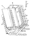
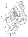
- the electrical connector 2 of the present embodiment can interconnect electrical traces 202 of a flat flexible cable, such as 200 to a printed circuit board 210.
- the electrical connector 2 generally comprises a housing 4 holding a plurality of electrical terminals 150, and further comprises a cam member 100 which can be rotated in the counter-clockwise direction (as viewed in Figure 1) to deflect the terminals to a position where the flexible cable 200 can be inserted without an insertion force.
- This type of electrical connector is usually referred to as a zero insertion force or ZIF electrical connector.
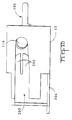
- the housing 4 is generally comprised of an insulating material such as a glass filled thermoplastic and generally includes a top wall 6, a recessed surface 8, a rear surface 10, a lower mounting surface 12, side walls 14 and 16 and a front mating face 18.
- the housing further comprises a plurality of ribs 24 which extend from a position proximate the front face 18 to the rear surface 10.
- the profile of the ribs at the front edge is defined by slanted edges 26, and by a plurality of side by side semi-circular edges 28.
- the housing 4 further comprises a plurality of apertures 50 which are in side by side alignment with the terminal receiving cavities 54.
- the cavities 54 are defined by side surfaces 56 and 58 as shown in Figure 2.
- the terminal receiving cavities 54 are defined by side surfaces 56 and 58 where the side surface 56 is co-planar with the side of the aperture 50 and with the side surfaces of the ribs 24. Although the side surface 56 is shown, due to the positioning of the cross-section, it should be appreciated that side surface 58 is a mirror image of the cross-section shown in Figure 6, and having the same co-planarity.
- the substrate receiving slot 20 can be seen as extending in a transverse direction across the front face 18 of the housing 4.
- the slot is defined by an upper surface 34 and a lower surface 40, and further defined by a plurality of elongate longitudinal ribs 36 and 42.
- the ribs 36 and 42 are alternately spaced according to the location of the terminals as best shown in Figure 4, and help to align the vertical position of the substrate with the contact portions of the terminals.
- the housing 4 includes apertures 84 therethrough for retaining the cam member 100 to the housing body.
- the apertures 84 are defined by two cut-out sections 80 and 82 which are laterally offset from one another and opening in opposite directions.
- the apertures 84 are created by two retractable mold parts which, when fully inserted, are flush to one another thereby forming the openings 84, and when retracted, they form the cut-out sections 80 and 82.
- a further slot 70 is formed behind the cut-out 80 and is defined by surfaces 72 and 74.
- the webs 27 and 29 are shown, which retain the sidewalls 14 and 16 to the remainder of the housing body.
- the cam member 100 includes a cylindrical portion 102 integral with a plate portion 110.
- the cam member 100 includes a plurality of side by side individual cam members 106 having arcuate surfaces 104 between each of the individual cam members 106.
- the plate member 110 includes an upper 114 and lower 112 surface, and a window 108 aligned with each of the cam members 106.
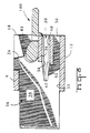
- a terminal 150 is shown as including a horizontal base section 152 having contact parts 172 and 174 extending therefrom in a vertical direction and a surface mount portion 176 extending in a horizontal direction from the base portion 152.
- the contact parts 172, 174 or 176 can be selectively retained depending on the type of electrical connection desired to the printed circuit board.
- a retention arm 168 extends from the front portion of the horizontal base section 152 and includes a first contact portion 166.
- a vertical leg 154 extends upwardly from the horizontal base portion 152 and is continuous through a U-shaped section 156 to a contact arm section 158.
- a lever arm 162 is continuous with the contact arm 158 and has at its lower section, a second contact portion 164.
- the cam member 100 is inserted into the nest area 22 of the housing such that the end sections 116 of the cam member 100 reside within the apertures 84 in the housing sidewalls.
- the plate portion 110 of the cam member is rotatable between two positive stops, between the positions where the lower surface 112 of the plate portion is in contact with the upper surface 32 of the platform 30 and, to a position where the surface 114 of the plate portion 110 is in abutting relation with the slanted surfaces 26 of the housing.
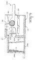
- the terminal is then stamped to the configuration shown in Figure 9 including all three legs 172, 174 and 176, and with the retention arm 168 and contact portion 166 extending at an acute angle relative to the horizontal base section 152.
- the terminals can then be plated to provide an electrically conductive surface at the contact points 164 and 166. It should be noted that when the terminal is stamped into the configuration of Figure 9, the contact points 164 and 166 are separated a sufficient distance that the terminals can be adequately plated along the sheared edges of the contacts.
- the retention arm 168 and contact point 166 are rotated in the counterclockwise direction (as viewed in Figure 9) until the contact point 166 moves into contact with the opposed contact section 164, and is further rotated until the contact portion 164 is slightly deflected thereby preloading the opposed contact portions 164 and 166 together.
- the section 170 of the terminal is of a reduced cross section relative to the remainder of the terminal which facilitates the bending of the terminal at the precise desired location, and without undue stresses causing cracking.
- the desired material for use with the terminals is a phosphor-bronze alloy which can accommodate such bending.
- the plating is tin plating which has been found to be pliable enough to bend at the section 170 without cracking. Even if some cracking is present, the point which is rotated, that is about point 170, is remote from the contact area and will not effect the electrical characteristics.
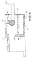
- the terminals can be stamped to accommodate either a through hole soldered connection or a surface mount connection.
- the soldered leads are staggered to provide a closer center line spacing of the edge stamped contacts.
- every other contact 150 would include a solder leg 172 whereas the remainder of the alternate contacts would include a through hole solder leg 174.
- each of the solder legs 172 and 174 are sheared clean of the stamped terminal and the surface mount lead 176 is retained.
- the terminals 150 are insertable into the electrical housing as shown in Figure 5.
- the retention arm 168 is receivable into the aperture 50 of the housing and interference fit to retain the terminals in position. Since the retention arm 168 is fixedly mounted within the aperture 50 and with the edge 178 in contact with the lower surface 51 of the aperture 50 as shown in Figure 5, the opposed contact portions 164, 166 ( Figure 9) will be retained in a prestressed condition. Said differently, the retention arm 168 will have a tendency, when not loaded in the housing, to relieve its original prestressed condition, by rotating in a clockwise direction about pivot point 170. However, the retention arm 168 and the horizontal base section 152 are being rigidly held in a fixed linear position by the aperture 50 which precludes the relaxation between the two opposed portions 164 and 166.
- the housing shown in Figure 2 has a height between surfaces 6 and 12 of only 4 millimeters, and the flat flexible cable which in interconnectable to the connector can vary between 0.1 and 0.3 millimeters, with the conductive elements on the cable at centerlines of only 0.0635 cm (0.025 inches).
- the first advantage, given the lowest height of the electrical connector, is that an actuator can be used which does not substantially increase the length of the overall connector. This has been accomplished by designing the cam member to have a very high mechanical advantage due to the large rotation angle of the camming member between the two stops as previously described.
- windows 108 are provided in the plate member in alignment with each of the cam members. After the lever arm 162 passes over the cam surface 106, the lever arm 162 actually passes through the windows 108 increasing the rotation angle of the camming member, and resultantly, the mechanical advantage.
- the windows 108 also provide for the second advantage, that when the cam member 100 is rotated to its full upright position to a position where the levers 162 project through the windows 108 as shown in Figure 4, the spring force on the upper contact arm 158 due to its deflected position bears on the cam member retaining the cam member in an upward position. This force holds the cam actuator 100 in position, which also holds the contacts to a deflected condition poised for insertion of the cable.
- a third advantage of the camming feature is that a rib 26 is positioned within each of the circular sections 104 which in turn positions each of the cam members 106 within one of the recesses 54 which retains the cam members 106 in side to side alignment with the lever portions 162 of the terminals. This ensures that the lever portions are retained within the recesses 54 and in alignment with the cam portions 105.
- the connector has been designed for either through hole or surface mounting.
- a retention feature 200 is used, as shown in Figures 1, 2 and 7, which is insertable into the recess 70 and can be latched in place.
- the retention member 200 includes two bifurcate arms 202 where the lower arm has a latching shoulder, which when in the fully inserted position, can be latched behind a shoulder 204 of the web 29.
- the retention member 200 includes a foot which can then be soldered to the board which retains the connector in position on the board.
- a through hole post could also be provided extending from the retention member which is soldered or otherwise latched to the printed circuit board.
- a shielded version is available, where the same housing is used for both the shielded and unshielded version.
- an optional shield member 300 can be added to the connector 2, which comprises an upper shield wall 302 and shielding sidewalls 304.
- a rear shield wall is also provided which extends between the upper wall 302 and between the sidewalls 304, although due to the angle of the isometric view of Figure 11, the rear wall cannot be seen.
- two retention arms 308 are provided, which are sheared away from the sidewalls 304 about shear lines 306.
- the ends of the retention arms 308 include latching features 310 identical to the latching features 202 ( Figure 7), and can be latched to the latching shoulder 204 as shown in Figure 11.
- the availability of the shielding version is quite advantageous, and is due to the quite efficient design of the electrical connector shown in Figure 1.
- the camming member 100 due to the very efficient camming member 100, the camming member is very small dimensionally when compared to the rest of the connector housing. Also, the camming member only operates in a very small portion of the connector housing, leaving the rest of the connector housing to be shielded.
- the shield member shown in Figure 11 could also include such features as through hole posts which are connectable to ground traces on the printed circuit boards.
- the exact same housing can be used with several differently configured systems.
- the cam member of the electrical connector is very small relative to the remainder of the connector due to the high mechanical advantage of the connector.
- the connector can be configured as a horizontal through hole version, a horizontal surface mount version, a vertical through hole version or a vertical surface mount version.
- the terminals are designed such that the same stamping for the horizontal version, and the same terminal stamping for the vertical version can be used to make either the through hole or surface mount connector.
- any of the above mentioned configurations can be electrically shielded.
Landscapes
- Coupling Device And Connection With Printed Circuit (AREA)
- Manufacturing Of Electrical Connectors (AREA)
Claims (10)
- Verfahren zum Herstellen kantengestanzter elektrischer Anschlüsse (150) für einen elektrischen Verbinder zum Herstellen einer elektrischen Verbindung zwischen einem Substrat (210), das gedruckte Schaltkreise trägt, und weiteren leitfähigen Elementen, (202), wobei der Verbinder (2) ein isolierendes Gehäuse (4) umfaßt, das eine Vielzahl von Anschlußdurchgängen (56) zur Aufnahme einer Vielzahl der kantengestanzten elektrischen Anschlüsse (150) aufweist, und wobei die elektrischen Anschlüsse (150) gegenüberliegende Kontaktglieder (164, 166) haben, die die elektrische Verbindung mit den weiteren leitfähigen Elementen (202) bewirken, wobei das Verfahren den folgenden Schritt aufweist:
- Kantenstanzen der Anschlüsse (150) zur Bildung eines waagerechten Hauptteils (152) mit einem Federarm (158), der sich von dem Hauptteil (152) nach oben erstreckt, und mit einem Verlängerungsarm (168), der sich von dem Federarm (158) weg erstreckt. wobei der Verlängerungsarm (168) ein erstes Kontaktglied (166) hat. das sich davon nach oben auf den Federarm (158) zu erstreckt, und wobei der Federarm (158) ein zweites Kontaktglied (164) trägt, das von dem ersten Kontaktglied (166) beabstandet ist,
gekennzeichnet durch die weiteren Schritte- Ausbilden des Verlängerungsarmes (168) derart, daß er sich in der entgegengesetzten Richtung wie der Federarm (158) und unter einem spitzen Winkel in bezug auf den Hauptteil (152) erstreckt, so daß das erste Kontaktglied (166) anfänglich von dem zweiten Kontaktglied (164) entfernt ist, und- anschließendes Biegen des Verlängerungsarms (168) durch plastisches Verformen eines Verbindungsabschnitts (170) zwischen dem Verlängerungsarm (168) und dem Hauptteil (152), um den Verlängerungsarm (168) auf den Federarm (158) zu in eine neue Position zu bewegen, in der das erste Kontaktglied (166) und das zweite Kontaktglied (164) einander gegenüber liegen und aufeinander zu weisen. - Verfahren nach Anspruch 1, dadurch gekennzeichnet, daß anschließend an den Schritt des Kantenstanzens, aber vor dem Schritt des Biegens des Verlängerungsarms (168), das erste Kontaktglied (166) und das zweite Kontaktglied (164) plattiert werden.
- Verfahren nach Anspruch 1 oder 2, dadurch gekennzeichnet, daß der Verlängerungsarm (168) auf den Federarm (158) zu in einem Maß gebogen wird, daß das erste Kontaktglied (166) und das zweite Kontaktglied (164) gegeneinander vorgespannt werden.
- Elektrischer Verbinder mit kantengestanzten Anschlüssen (150), die nach dem Verfahren gemäß einem der Ansprüche 1 bis 3 hergestellt sind, dadurch gekennzeichnet, daß das Gehäuse (4) eine Vielzahl von Öffnungen (50) hat, die sich in dem Gehäuse (4) erstrecken und die Verlängerungsarme (168) aufnehmen.
- Elektrischer Verbinder nach Anspruch 4, dadurch gekennzeichnet, daß ein Substrataufnahmeschlitz (20) durch Mittel gebildet ist, die mit dem Gehäuse (4) einstückig sind. und der sich oberhalb und quer zu den Öffnungen (50) erstreckt.
- Elektrischer Verbinder nach Anspruch 4 oder 5, dadurch gekennzeichnet, daß die Anschlußaufnahmedurchgänge (56) durch einen Boden (51) gebildet sind. der sich nach vorn zu den Öffnungen (50) erstreckt.
- Elektrischer Verbinder nach Anspruch 6, dadurch gekennzeichnet, daß die untere Kante (178) des waagerechten Hauptteils (152) in Anlage mit dem Boden (51) ist.
- Elektrischer Verbinder nach einem der vorhergehenden Ansprüche, dadurch gekennzeichnet, daß der Verbindungsabschnitt jedes der Anschlüsse (150) einen verminderten Querschnitt (170) hat, um das Biegen zu erleichtern.
- Elektrischer Verbinder nach Anspruch 6, dadurch gekennzeichnet, daß der Boden (51) sich hinter den Verbindungsabschnitten (170) der Anschlüsse (150) erstreckt.
- Elektrischer Verbinder nach Anspruch 4, 5 oder 6, dadurch gekennzeichnet, daß die oberen Kanten der Verlängerungsarme (168) in Anlage mit den oberen Oberflächen der Öffnungen (50) sind, wodurch eine Gegenverdrehung des Verlängerungsarms (168) relativ zu dem waagerechten Hauptteil (152) verhindert ist.
Applications Claiming Priority (2)
| Application Number | Priority Date | Filing Date | Title |
|---|---|---|---|
| GB898904492A GB8904492D0 (en) | 1989-02-28 | 1989-02-28 | Electrical connector having preloaded terminals |
| GB8904492 | 1989-02-28 |
Publications (2)
| Publication Number | Publication Date |
|---|---|
| EP0385019A1 EP0385019A1 (de) | 1990-09-05 |
| EP0385019B1 true EP0385019B1 (de) | 1994-10-19 |
Family
ID=10652425
Family Applications (1)
| Application Number | Title | Priority Date | Filing Date |
|---|---|---|---|
| EP89304336A Expired - Lifetime EP0385019B1 (de) | 1989-02-28 | 1989-04-28 | Elektrischer Verbinder mit vorgespannten Kontakten und Verfahren zu dessen Herstellung |
Country Status (4)
| Country | Link |
|---|---|
| EP (1) | EP0385019B1 (de) |
| DE (1) | DE68918933T2 (de) |
| ES (1) | ES2061986T3 (de) |
| GB (1) | GB8904492D0 (de) |
Families Citing this family (6)
| Publication number | Priority date | Publication date | Assignee | Title |
|---|---|---|---|---|
| JP3391431B2 (ja) * | 1997-01-23 | 2003-03-31 | 住友電装株式会社 | シート状導電路用コネクタ |
| JP4151129B2 (ja) * | 1998-09-25 | 2008-09-17 | モレックス インコーポレーテッド | Fpc用コネクタ |
| KR100514596B1 (ko) * | 2003-08-27 | 2005-09-14 | 한국몰렉스 주식회사 | 가요성 케이블 커넥터용 액츄에이터 |
| JP4682706B2 (ja) * | 2005-05-31 | 2011-05-11 | オムロン株式会社 | コネクタ |
| JP4657160B2 (ja) * | 2006-06-22 | 2011-03-23 | ヒロセ電機株式会社 | 電気コネクタ |
| TWI657630B (zh) * | 2016-12-24 | 2019-04-21 | 英屬開曼群島商鴻騰精密科技股份有限公司 | 電連接器 |
Family Cites Families (3)
| Publication number | Priority date | Publication date | Assignee | Title |
|---|---|---|---|---|
| BE880356A (nl) * | 1979-11-30 | 1980-05-30 | Burndy Corp | Elektrische stekkerverbindingen met uitschakelbare indrukken uittrekkracht op de contacten |
| US4638559A (en) * | 1984-10-30 | 1987-01-27 | At&T Technologies, Inc. | Methods of and apparatus for making slotted beam contact elements |
| DE8626537U1 (de) * | 1986-10-03 | 1988-06-23 | Grote & Hartmann Gmbh & Co Kg, 5600 Wuppertal | Folienverbinder für gedruckte Schaltungen |
-
1989
- 1989-02-28 GB GB898904492A patent/GB8904492D0/en active Pending
- 1989-04-28 ES ES89304336T patent/ES2061986T3/es not_active Expired - Lifetime
- 1989-04-28 DE DE68918933T patent/DE68918933T2/de not_active Expired - Fee Related
- 1989-04-28 EP EP89304336A patent/EP0385019B1/de not_active Expired - Lifetime
Also Published As
| Publication number | Publication date |
|---|---|
| ES2061986T3 (es) | 1994-12-16 |
| DE68918933D1 (de) | 1994-11-24 |
| GB8904492D0 (en) | 1989-04-12 |
| DE68918933T2 (de) | 1995-05-24 |
| EP0385019A1 (de) | 1990-09-05 |
Similar Documents
| Publication | Publication Date | Title |
|---|---|---|
| US5173058A (en) | Zero insertion force electrical connector | |
| US5240430A (en) | Electrical connector for cable to circit board application | |
| EP0280449B1 (de) | An der Oberfläche montierbarer elektrischer Stecker | |
| EP0778990B1 (de) | Verriegelungs- und montageelement fuer einen oberflaechenmontierten elektrischen verbinder | |
| US5026292A (en) | Card edge connector | |
| EP0519264B1 (de) | Elektrischer Verbinder | |
| US5077893A (en) | Method for forming electrical terminal | |
| KR940011264B1 (ko) | 접지 구조물을 갖고 있는 커넥터 | |
| US5112233A (en) | Electrical connector having contact retention means | |
| EP0340730B1 (de) | Mehrfachkontaktanordnung zur Aufnahme der Kontaktkante einer dünnen gedruckten Schaltkarte sowie flexibles Kontaktelement für diesen Zweck | |
| EP0602443A2 (de) | Vorrichtung für die Befestigung eines Steckverbinders auf einer Leiterplatte | |
| US6039590A (en) | Electrical connector with relatively movable two-part housing | |
| US6866518B1 (en) | Electrical interconnection between multiple printed circuit boards | |
| EP0540260B1 (de) | Elektrischer Verbinder zur Verbindung einer Leiterplatte mit einem Kabel | |
| JPH09505435A (ja) | 直角電気コネクタおよびこれを挿入する部材 | |
| EP0340994B1 (de) | Einfügungskraftfreier elektrischer Verbinder | |
| EP0497554B1 (de) | Befestigungsteil | |
| EP0643450B1 (de) | Nockenbetätigte Flachbaubuchse mit Anschlüssen welche von einer Rippe gehalten werden | |
| EP0140473A1 (de) | Lötfreier elektrischer Leiter für gedruckte Schaltungen und Steckvorrichtung, die diesen verwendet | |
| US5597320A (en) | Zero insertion force electrical connector and terminal | |
| US5445529A (en) | Connector apparatus | |
| EP0385019B1 (de) | Elektrischer Verbinder mit vorgespannten Kontakten und Verfahren zu dessen Herstellung | |
| EP0109297B1 (de) | Elektrische Kontaktorgane und Zusammenbau elektrischer Verbinder | |
| EP0603161B1 (de) | Einfügungskraftfreier Verbinder für Anwendungen von Kabel zu Leiterplatte | |
| EP0400378B1 (de) | Leiterplattensockel mit Kleeblattkontakt |
Legal Events
| Date | Code | Title | Description |
|---|---|---|---|
| PUAI | Public reference made under article 153(3) epc to a published international application that has entered the european phase |
Free format text: ORIGINAL CODE: 0009012 |
|
| AK | Designated contracting states |
Kind code of ref document: A1 Designated state(s): DE ES FR GB IT NL |
|
| 17P | Request for examination filed |
Effective date: 19901227 |
|
| RAP1 | Party data changed (applicant data changed or rights of an application transferred) |
Owner name: THE WHITAKER CORPORATION |
|
| 17Q | First examination report despatched |
Effective date: 19930302 |
|
| GRAA | (expected) grant |
Free format text: ORIGINAL CODE: 0009210 |
|
| AK | Designated contracting states |
Kind code of ref document: B1 Designated state(s): DE ES FR GB IT NL |
|
| REF | Corresponds to: |
Ref document number: 68918933 Country of ref document: DE Date of ref document: 19941124 |
|
| REG | Reference to a national code |
Ref country code: ES Ref legal event code: FG2A Ref document number: 2061986 Country of ref document: ES Kind code of ref document: T3 |
|
| ITF | It: translation for a ep patent filed | ||
| ET | Fr: translation filed | ||
| PLBE | No opposition filed within time limit |
Free format text: ORIGINAL CODE: 0009261 |
|
| STAA | Information on the status of an ep patent application or granted ep patent |
Free format text: STATUS: NO OPPOSITION FILED WITHIN TIME LIMIT |
|
| 26N | No opposition filed | ||
| PGFP | Annual fee paid to national office [announced via postgrant information from national office to epo] |
Ref country code: ES Payment date: 19970424 Year of fee payment: 9 |
|
| PG25 | Lapsed in a contracting state [announced via postgrant information from national office to epo] |
Ref country code: ES Free format text: LAPSE BECAUSE OF NON-PAYMENT OF DUE FEES Effective date: 19980429 |
|
| PGFP | Annual fee paid to national office [announced via postgrant information from national office to epo] |
Ref country code: GB Payment date: 19990315 Year of fee payment: 11 |
|
| PGFP | Annual fee paid to national office [announced via postgrant information from national office to epo] |
Ref country code: NL Payment date: 19990322 Year of fee payment: 11 |
|
| PGFP | Annual fee paid to national office [announced via postgrant information from national office to epo] |
Ref country code: FR Payment date: 19990406 Year of fee payment: 11 |
|
| PGFP | Annual fee paid to national office [announced via postgrant information from national office to epo] |
Ref country code: DE Payment date: 19990430 Year of fee payment: 11 |
|
| PG25 | Lapsed in a contracting state [announced via postgrant information from national office to epo] |
Ref country code: GB Free format text: LAPSE BECAUSE OF NON-PAYMENT OF DUE FEES Effective date: 20000428 |
|
| REG | Reference to a national code |
Ref country code: ES Ref legal event code: FD2A Effective date: 20000503 |
|
| PG25 | Lapsed in a contracting state [announced via postgrant information from national office to epo] |
Ref country code: NL Free format text: LAPSE BECAUSE OF NON-PAYMENT OF DUE FEES Effective date: 20001101 |
|
| GBPC | Gb: european patent ceased through non-payment of renewal fee |
Effective date: 20000428 |
|
| PG25 | Lapsed in a contracting state [announced via postgrant information from national office to epo] |
Ref country code: FR Free format text: LAPSE BECAUSE OF NON-PAYMENT OF DUE FEES Effective date: 20001229 |
|
| NLV4 | Nl: lapsed or anulled due to non-payment of the annual fee |
Effective date: 20001101 |
|
| PG25 | Lapsed in a contracting state [announced via postgrant information from national office to epo] |
Ref country code: DE Free format text: LAPSE BECAUSE OF NON-PAYMENT OF DUE FEES Effective date: 20010201 |
|
| REG | Reference to a national code |
Ref country code: FR Ref legal event code: ST |
|
| PG25 | Lapsed in a contracting state [announced via postgrant information from national office to epo] |
Ref country code: IT Free format text: LAPSE BECAUSE OF NON-PAYMENT OF DUE FEES;WARNING: LAPSES OF ITALIAN PATENTS WITH EFFECTIVE DATE BEFORE 2007 MAY HAVE OCCURRED AT ANY TIME BEFORE 2007. THE CORRECT EFFECTIVE DATE MAY BE DIFFERENT FROM THE ONE RECORDED. Effective date: 20050428 |