EP0385252A2 - Appareil pour commander une voiture électrique - Google Patents
Appareil pour commander une voiture électrique Download PDFInfo
- Publication number
- EP0385252A2 EP0385252A2 EP90103332A EP90103332A EP0385252A2 EP 0385252 A2 EP0385252 A2 EP 0385252A2 EP 90103332 A EP90103332 A EP 90103332A EP 90103332 A EP90103332 A EP 90103332A EP 0385252 A2 EP0385252 A2 EP 0385252A2
- Authority
- EP
- European Patent Office
- Prior art keywords
- circuit
- brake
- control
- output
- resistor
- Prior art date
- Legal status (The legal status is an assumption and is not a legal conclusion. Google has not performed a legal analysis and makes no representation as to the accuracy of the status listed.)
- Granted
Links
- 230000001133 acceleration Effects 0.000 claims description 39
- 238000010276 construction Methods 0.000 description 17
- 238000010586 diagram Methods 0.000 description 13
- 239000003990 capacitor Substances 0.000 description 9
- 230000007423 decrease Effects 0.000 description 5
- 230000001934 delay Effects 0.000 description 2
- 210000004899 c-terminal region Anatomy 0.000 description 1
- 238000000034 method Methods 0.000 description 1
- 238000010248 power generation Methods 0.000 description 1
- 238000007493 shaping process Methods 0.000 description 1
- 230000035939 shock Effects 0.000 description 1
Images


Classifications
-
- B—PERFORMING OPERATIONS; TRANSPORTING
- B60—VEHICLES IN GENERAL
- B60L—PROPULSION OF ELECTRICALLY-PROPELLED VEHICLES; SUPPLYING ELECTRIC POWER FOR AUXILIARY EQUIPMENT OF ELECTRICALLY-PROPELLED VEHICLES; ELECTRODYNAMIC BRAKE SYSTEMS FOR VEHICLES IN GENERAL; MAGNETIC SUSPENSION OR LEVITATION FOR VEHICLES; MONITORING OPERATING VARIABLES OF ELECTRICALLY-PROPELLED VEHICLES; ELECTRIC SAFETY DEVICES FOR ELECTRICALLY-PROPELLED VEHICLES
- B60L7/00—Electrodynamic brake systems for vehicles in general
- B60L7/28—Eddy-current braking
-
- Y—GENERAL TAGGING OF NEW TECHNOLOGICAL DEVELOPMENTS; GENERAL TAGGING OF CROSS-SECTIONAL TECHNOLOGIES SPANNING OVER SEVERAL SECTIONS OF THE IPC; TECHNICAL SUBJECTS COVERED BY FORMER USPC CROSS-REFERENCE ART COLLECTIONS [XRACs] AND DIGESTS
- Y02—TECHNOLOGIES OR APPLICATIONS FOR MITIGATION OR ADAPTATION AGAINST CLIMATE CHANGE
- Y02T—CLIMATE CHANGE MITIGATION TECHNOLOGIES RELATED TO TRANSPORTATION
- Y02T10/00—Road transport of goods or passengers
- Y02T10/60—Other road transportation technologies with climate change mitigation effect
- Y02T10/72—Electric energy management in electromobility
Definitions
- the invention relates to an apparatus for controlling an electric motor car.
- the present invention relates to an apparatus for braking an electric motor car and, more particularly, to an electric motor car braking apparatus having a magnet brake of non-exciting operating type.
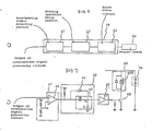
- FIG. 5 shows a whole construction of a general electric motor car
- Fig. 6 shows a brake control section in the construction of Fig. 5
- Fig. 7 shows an example of a practical construction of the brake control section.
- the conventional example shown in Fig. 5 comprises: an accelerator 51 as a control terminal; an acceleration signal processing circuit 52 for processing an output signal of a variable resistor (not shown) attached to the accelerator 51 and generating an acceleration signal; a rotational speed control circuit 53 provided at an output stage of the acceleration signal processing circuit 52; a pulse width modulating circuit (hereinafter, referred to as a "PWM circuit") 54 provided at an output stage of the rotational speed control circuit 53; and a motor drive circuit 55 to generate a drive current to a drive motor 56 at the next stage in accordance with an output signal of the PWM circuit 54.
- the drive motor 56 is provided with motor rotational speed detecting means 57.
- a rotational speed of the drive motor 56 is detected and the result is fed back to the rotational speed control circuit 53. Therefore, the rotational speed control circuit 53 outputs a control signal to the PWM circuit 54 so as to make the drive motor follow the acceleration signal.
- the PWM circuit 54 is provided with a PWM oscillator 58 to generate a reference triangular wave (or saw-tooth wave) for what is called a chopping control.
- the PWM circuit 54 executes chopping control by a reference triangular wave to an output signal of the rotational speed control circuit 53 and outputs a drive control signal.
- a brake control section 59 to generate a control signal to a magnet brake 60 (which will be explained hereinlater) in accordance with the acceleration signal is provided at an output stage of the acceleration signal processing circuit 52.
- the brake control section 59 comprises: an acceleration signal detecting circuit 61 for detecting the on/off of the acceleration signal which is output from the acceleration signal processing circuit 52 and outputting a brake-on control signal or a brake-off control signal; a braking operation delay circuit 62 which is provided at an output stage of the acceleration signal detecting circuit 61 and delays only the brake-on control signal by a predetermined time; and a brake drive circuit 63 which is provided at an output stage of the braking operation delay circuit 62 and makes a brake operative or inoperative on the basis of the brake-on/off control signals.
- the brake control section 59 executes a brake control in the case of using the magnet brake 60 of the non-exciting operating type, in which a fail safe is realized so as to turn off the brake only in the current supplying state and to always turn on the brake in the non-current supplying state in order to control an electric motor car.
- the acceleration signal detecting circuit 61 has a comparator 64 for comparing the level of the acceleration signal with a predetermined threshold value V r and generating an output.
- the braking operation delay circuit 62 comprises: an integrating circuit 65 which is constructed by a resistor R1 and a capacitor C1; and a diode 66.
- the brake drive circuit 63 has an buffer 67 by waveform shaping an output of the braking operation delay circuit 62 and outputting to a transistor 68 for a current supply control of a brake coil 60a of the magnet brake 60.
- an output of the comparator 64 is set to the "high (H)" level. Since a voltage in the forward direction is applied to the diode 66, the capacitor C1 is promptly charged by bypassing the resistor R1. V c is set to the level to turn on the brake drive circuit 63. In other words, the input level of the buffer 67 is set to the "low (L)” level. Therefore, the output of the buffer 67 is set to the "H” level.
- a transistor 68 is made conductive.
- the brake coil 60a is excited by a current from a battery 70. The magnet brake 60 is turned off.
- the output of the comparator 64 is set to the "low (L)" level and the charges stored in the capacitor C1 are discharged through the resistor R1 and V c gradually decreases. Therefore, after the elapse of a predetermined time, the input level of the buffer 67 is set to the "L” level. The output of the buffer 67 is set to the "L” level.
- the brake coil 60a is not energized. The magnet brake 60 is turned on. In this manner, simultaneously with the turn-on of the accelerator, the brake is turned on after the elapse of a predetermined time from the brake-off and accelerator-off.
- the delay time from the accelerator-off to the brake-on is determined by the capacitance of the capacitor C1 and the resistance value of the resistor R1, it is always constant. Therefore, there occurs an inconvenience such that by setting so as to smoothly stop from a certain predetermined speed, a stop shock increases when it is faster than that speed, and if it is contrarily slower than that speed, the braking operation is likely to be executed with a delay time and the braking distance increases.
- the invention comprises: an acceleration signal detecting circuit for detecting the on/off of an acceleration signal from a control terminal and outputting a brake-on control signal or a brake-off control signal; and a brake drive circuit for making a brake operative or inoperative on the basis of the brake-on/off control signal.
- a braking operation delay circuit to delay only the brake-on control signal by a predetermined time is provided between those circuits.
- the braking operation delay circuit is provided with a delay time correcting circuit for variably setting a delay time of the braking operation delay circuit in accordance with the rotational speed of the drive motor of the electric motor car. Due to this, the above object is accomplished.
- the present invention relates to an apparatus for controlling a drive motor of an electric motor car and, more particularly, to a drive motor control apparatus of an electric motorcar which is suitable for a motorcar having a high/low speed change-over switch.
- Figs. 12 to 14 show a conventional example.
- Fig. 12 shows a general construction of an apparatus for controlling a drive motor of an electric motorcar having an electrical variable speed switch
- Fig.13 shows a high/low speed switching section in Fig. 12
- Fig. 14 shows a torque-rotational speed characteristics in the full opening mode of an accelerator in Fig. 13.
- the conventional example shown in Fig. 12 comprises: an acceleration signal processing circuit 52 for processing an output signal of a variable resistor (not shown) attached to an accelerator (not shown) and for generating an acceleration signal; a high/low speed switching section 40 provided at the output stage of the acceleration signal processing circuit 52 ; a pulse width modulating circuit (hereinafter, referred to as a "PWM circuit") 54 provided at the output stage of the high/low speed switching section 40 ; and a motor drive circuit 55 for generating a drive current to a drive motor 56 at the next stage in accordance with an output signal of the PWM circuit 54.
- PWM circuit pulse width modulating circuit
- An oscillator 58 for PWM to generate a reference triangular wave (or a saw-tooth wave) for what is called a chopping control is provided for the PWM circuit 54.
- the PWM circuit 54 executes the chopping control to an output of the high/low speed switching section 40 by the reference triangular wave and outputs a motor drive control signal.
- the high/low speed switching section 40 comprises: a first resistor 41 connected to the output stage of the acceleration signal processing circuit 52 ; a second resistor 42 to voltage divide the output of the acceleration signal processing circuit 52 together with the resistor 41; and a high/low speed change-over switch 43 serving as speed switching means connected to the resistor 42.
- the invention has a first resistor and a second resistor for voltage dividing an acceleration signal from a control terminal and speed switching means provided for the second resistor.
- a predetermined control of the drive motor of the motorcar is executed on the basis of a voltage division output.
- Circuit on/off means for turning on and off the second resistor and the speed switching means is arranged therebetween.
- An on/off control circuit to on/off control the circuit on/off means in accordance with a rotational speed of the drive motor is provided for the circuit on/off means. Due to this the above object is accomplished.
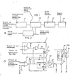
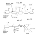
- the embodiment shown in Fig. 1 comprises: the acceleration signal detecting circuit 61 for detecting the on/off of an acceleration signal which is output from the acceleration signal processing circuit 52 and outputting a brake-on control signal or a brake-off control signal; a braking operation delay circuit 62 which is provided at an output stage of the acceleration signal detecting circuit 61 and delays only the brake-on control signal by a predetermined time; and a brake drive circuit 63 as a brake driving circuit which is provided at an output stage of the braking operation delay circuit 62 and makes the brake operative or inoperative on the basis of the brake-on/off control signals.
- the braking operation delay circuit 62 is provided with a delay time correcting circuit 1 for variably setting the delay time of the braking operation delay circuit 62 in accordance with the rotational speed of the drive motor 56 for the electric motor car.
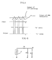
- the delay time correcting circuit 1 comprises: a comparator 2 for comparing an F/V converter output which is proportional to the rotational speed of the drive motor 56 with an output of the oscillator 58 for PWM and outputting a square wave having a duty corresponding to the motor rotational speed as shown in Fig. 3; an OR circuit 3 for outputting the OR of an output of the comparator 2 and an output of the comparator 64 to compare the acceleration signal and the predetermined threshold value V r ; a resistor R2 connected to an output terminal of the OR circuit 3; and a diode 4 whose cathode side is connected to the resistor R2 and whose anode side is connected to the cathode side of the diode 66 mentioned above.
- the output of the comparator 64 is set to the "high (H)" level. Since a voltage in the forward direction is applied to the diode 66, the capacitor C1 is promptly charged by bypassing the resistor R1. V c is set to such a level as to turn on the brake drive circuit 63. In other words, the input level of the buffer 67 is set to the "H” level. Therefore, an output of the buffer 67 is set to the "H” level. the transistor 68 is made conductive, the brake coil 60a is energized, and the magnet brake 60 is turned off. At this time, since the output of the OR circuit 3 is always at the "H” level, the diode 4 is reversed and the delay time correcting circuit 1 does not exert any influence on the braking operation delay circuit 62.
- a switch 5 closes the contact when the output of the comparator 2, i.e., the output of the OR circuit 3 is set to the "L” level.
- the contact is opened when it is set to the "H” level.
- the delay time changes in a range from a time constant R1C1 to R1R2/(R1+R2) ⁇ C1 in accordance with the motor rotational speed.
- the input level of the buffer 67 is set to the "L” level
- the output of the buffer 67 is set to the "L” level
- the brake coil 60a is not energized
- the magnet brake 60 is turned on.
- the magnet brake 60 As described above, according to the embodiment, as the rotational speed of the drive motor 56 is low, the magnet brake 60 is rapidly turned on. As the rotational speed is high, the magnet brake 60 is slowly turned on, in other words, there is an advantage such that since the time from the turn-off of the accelerator to the turn-on of the brake continuously changes in accordance with the rotational speed of the motor, that is, the velocity, it is possible to smoothly stop without being largely influenced by the velocity. On the other hand, even when the power generation brake fails or the motor is not decelerated after the turn-off of the accelerator in the case of a down slope or the like, the magnet brake 60 is turned on after the elapse of the longest delay time which is determined by the time constant R1C1.
- the delay time of the braking operation delay circuit can be variably set in accordance with the rotational speed of the drive motor by the function of the delay time correcting circuit provided for the braking operation delay circuit, so that as in the above embodiment, as the rotational speed of the drive motor is low, the brake is rapidly turned on, while as the rotational speed is high, the brake is slowly turned on, and therefore, the time from the turn-off of the accelerator to the turn-on of the brake can be continuously changed in accordance with the velocity, and the motor car can be smoothly stopped without being largely influenced by the velocity.
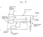
- the embodiment shown in Fig. 8 comprises: the acceleration signal processing circuit 52 for processing an output signal of a variable resistor (not shown) attached to an accelerator (not shown) as a control terminal and for generating an acceleration signal; the first resistor 41 and the second resistor 42 for voltage dividing the acceleration signal; an analog switch 20 serving as circuit on/off means connected to the second resistor 42 ; and the high/low speed change-over switch 43 serving as speed switching means in which one end is connected to the analog switch 20 and the other end is connected to the ground.
- the analog switch 20 turns on and off the circuit between the second resistor 42 and the high/low speed change-over switch 43.
- An on/off control circuit 21 to on/off control the analog switch 20 in accordance with the rotational speed of the drive motor 56 is provided for the analog switch 20.
- the on/off control circuit 21 comprises: a rotational speed signal output circuit 22 to output a voltage signal which is proportional to the rotational speed of the drive motor 56; an oscillator 23 for PWM to output a reference triangular wave (or a saw-tooth wave); and a PWM circuit 24 for executing a PWM control to an output of the rotational speed signal output circuit 22 by the reference triangular wave and for outputting an on/off control signal to the analog switch 20.
- the rotational speed signal output circuit 22 comprises: a rotational speed-pulse converter 25 provided for the drive motor 56 ; and an F/V converter 26 for converting an output signal of the rotational speed-pulse converter 25 into a voltage signal.
- a comparator 27 shown in Fig. 9 is actually used in the PWM circuit 24.
- the other construction is the same as that in the foregoing conventional example.
- the operating mode is gradually set into the low speed mode.
- a rotational speed signal output circuit 30 is constructed by: a shunt resistor 28 which is connected to the drive motor 56 and converts a motor current i M into a voltage; and an amplifier 29 to amplify the output voltage of the shunt resistor 28.
- the PWM oscillator 23 is connected to the plus side contrarily with the above embodiment. The other construction is the same as the above embodiment.
- Fig. 11 shows torque-current and rotational speed characteristics in the full opening mode of the accelerator in this case.
- a state in which the motor is difficult to rotate due to a high load can be presumed from the motor current i M . Therefore, such a current is used. That is, since the motor current i M is large in the low speed mode and the output of the comparator 27 is at the "L" level, the circuit between the I and O terminals of the analog switch is not conductive. Therefore, even when the high/low speed change-over switch 43 is "on (low speed)" in a manner similar to the above embodiment, the operating mode is not set into the low speed mode. A drive current of the drive motor 56 when the motor drive circuit 55 is in the high speed mode is generated.
- the invention is constructed and functions as mentioned above, according to the invention, an excellent apparatus for controlling a drive motor of an electric motorcar which cannot be obtained hitherto can be obtained, in which due to the operation of the on/off control circuit provided for the circuit on/off means, the circuit on/off means can be opened when the rotational speed of the drive motor is zero or extremely small, and it can be gradually closed with an increase in rotational speed, even in a situation in which a torque is particularly needed in the case where the high/low speed change-over switch serving as speed switching means is set to "low speed", the motorcar can be easily started in a manner similar to the ordinary state, and for instance, if the apparatus is constructed as in the above embodiments, the sufficient effects can be obtained by merely adding a simple circuit without adding a complicated circuit for the rotational speed control.
Landscapes
- Engineering & Computer Science (AREA)
- Power Engineering (AREA)
- Transportation (AREA)
- Mechanical Engineering (AREA)
- Electric Propulsion And Braking For Vehicles (AREA)
Priority Applications (1)
| Application Number | Priority Date | Filing Date | Title |
|---|---|---|---|
| EP93119363A EP0600465B1 (fr) | 1989-02-28 | 1990-02-21 | Appareil pour commander un véhicule à moteur électrique |
Applications Claiming Priority (4)
| Application Number | Priority Date | Filing Date | Title |
|---|---|---|---|
| JP1047348A JP2827253B2 (ja) | 1989-02-28 | 1989-02-28 | 電動車輌の駆動用モータ制御装置 |
| JP47347/89 | 1989-02-28 | ||
| JP47348/89 | 1989-02-28 | ||
| JP4734789A JP2757201B2 (ja) | 1989-02-28 | 1989-02-28 | 電動車輌の制動装置 |
Related Child Applications (2)
| Application Number | Title | Priority Date | Filing Date |
|---|---|---|---|
| EP93119363A Division EP0600465B1 (fr) | 1989-02-28 | 1990-02-21 | Appareil pour commander un véhicule à moteur électrique |
| EP93119363.5 Division-Into | 1993-12-01 |
Publications (3)
| Publication Number | Publication Date |
|---|---|
| EP0385252A2 true EP0385252A2 (fr) | 1990-09-05 |
| EP0385252A3 EP0385252A3 (fr) | 1992-04-15 |
| EP0385252B1 EP0385252B1 (fr) | 1995-04-26 |
Family
ID=26387511
Family Applications (1)
| Application Number | Title | Priority Date | Filing Date |
|---|---|---|---|
| EP90103332A Expired - Lifetime EP0385252B1 (fr) | 1989-02-28 | 1990-02-21 | Appareil pour commander une voiture électrique |
Country Status (2)
| Country | Link |
|---|---|
| EP (1) | EP0385252B1 (fr) |
| DE (1) | DE69018857T2 (fr) |
Cited By (1)
| Publication number | Priority date | Publication date | Assignee | Title |
|---|---|---|---|---|
| CN114043876A (zh) * | 2021-11-09 | 2022-02-15 | 中国铁道科学研究院集团有限公司 | 基于涡流制动的列车制动系统 |
Family Cites Families (2)
| Publication number | Priority date | Publication date | Assignee | Title |
|---|---|---|---|---|
| US2525507A (en) * | 1949-01-14 | 1950-10-10 | Westinghouse Electric Corp | Automatic control for booster relay on electric vehicles |
| JPS5244712U (fr) * | 1975-09-25 | 1977-03-30 |
-
1990
- 1990-02-21 DE DE69018857T patent/DE69018857T2/de not_active Expired - Fee Related
- 1990-02-21 EP EP90103332A patent/EP0385252B1/fr not_active Expired - Lifetime
Cited By (2)
| Publication number | Priority date | Publication date | Assignee | Title |
|---|---|---|---|---|
| CN114043876A (zh) * | 2021-11-09 | 2022-02-15 | 中国铁道科学研究院集团有限公司 | 基于涡流制动的列车制动系统 |
| CN114043876B (zh) * | 2021-11-09 | 2024-01-26 | 中国铁道科学研究院集团有限公司 | 基于涡流制动的列车制动系统 |
Also Published As
| Publication number | Publication date |
|---|---|
| DE69018857D1 (de) | 1995-06-01 |
| DE69018857T2 (de) | 1995-08-24 |
| EP0385252B1 (fr) | 1995-04-26 |
| EP0385252A3 (fr) | 1992-04-15 |
Similar Documents
| Publication | Publication Date | Title |
|---|---|---|
| US5708343A (en) | Control device for direct current electric motor | |
| US4401926A (en) | Pulse controllers | |
| EP0510527A1 (fr) | Circuit de surveillance pour un système de recharge de la batterie d'un véhicule à moteur | |
| EP0743751A3 (fr) | Dispositif semi-conducteur | |
| JPS6243403B2 (fr) | ||
| US4114076A (en) | Control system for a motor having a shunt field winding | |
| US4503937A (en) | Elevator control circuit | |
| JPH04500399A (ja) | 電磁負荷を駆動する回路装置 | |
| US5218339A (en) | Arrangement for monitoring a consumer in combination with an internal combustion engine and/or a motor vehicle | |
| US4211965A (en) | Device for controlling rotational speed of electric motor | |
| EP0385252A2 (fr) | Appareil pour commander une voiture électrique | |
| JP2001500359A (ja) | 発電機レギュレータ | |
| EP0600465B1 (fr) | Appareil pour commander un véhicule à moteur électrique | |
| EP3460976B1 (fr) | Système de commande pour commander un circuit convertisseur de tension continue-continue | |
| US4636912A (en) | Circuit for controlling solenoid clutch | |
| US20010019493A1 (en) | Power output circuit having a pluse-width modulation mode and a permanently closed mode | |
| US4347467A (en) | Control circuit for a D.C. motor | |
| JPS6242457B2 (fr) | ||
| US4345190A (en) | Chopper control system | |
| JP2757201B2 (ja) | 電動車輌の制動装置 | |
| EP0501036B1 (fr) | Appareil de commande de vitesse pour véhicules électriques | |
| JP2701340B2 (ja) | 電気車の回生制動制御回路 | |
| JP2929826B2 (ja) | Gtoサイリスタゲート駆動回路 | |
| JPH0223045Y2 (fr) | ||
| US4079270A (en) | Gate control apparatus |
Legal Events
| Date | Code | Title | Description |
|---|---|---|---|
| PUAI | Public reference made under article 153(3) epc to a published international application that has entered the european phase |
Free format text: ORIGINAL CODE: 0009012 |
|
| AK | Designated contracting states |
Kind code of ref document: A2 Designated state(s): DE FR GB NL |
|
| 17P | Request for examination filed |
Effective date: 19901227 |
|
| PUAL | Search report despatched |
Free format text: ORIGINAL CODE: 0009013 |
|
| RAP1 | Party data changed (applicant data changed or rights of an application transferred) |
Owner name: SUZUKI MOTOR CORPORATION |
|
| AK | Designated contracting states |
Kind code of ref document: A3 Designated state(s): DE FR GB NL |
|
| 17Q | First examination report despatched |
Effective date: 19930525 |
|
| GRAA | (expected) grant |
Free format text: ORIGINAL CODE: 0009210 |
|
| AK | Designated contracting states |
Kind code of ref document: B1 Designated state(s): DE FR GB NL |
|
| XX | Miscellaneous (additional remarks) |
Free format text: TEILANMELDUNG 93119363.5 EINGEREICHT AM 21/02/90. |
|
| REF | Corresponds to: |
Ref document number: 69018857 Country of ref document: DE Date of ref document: 19950601 |
|
| ET | Fr: translation filed | ||
| PLBE | No opposition filed within time limit |
Free format text: ORIGINAL CODE: 0009261 |
|
| STAA | Information on the status of an ep patent application or granted ep patent |
Free format text: STATUS: NO OPPOSITION FILED WITHIN TIME LIMIT |
|
| 26N | No opposition filed | ||
| REG | Reference to a national code |
Ref country code: GB Ref legal event code: IF02 |
|
| PGFP | Annual fee paid to national office [announced via postgrant information from national office to epo] |
Ref country code: FR Payment date: 20030210 Year of fee payment: 14 |
|
| PGFP | Annual fee paid to national office [announced via postgrant information from national office to epo] |
Ref country code: GB Payment date: 20030219 Year of fee payment: 14 |
|
| PGFP | Annual fee paid to national office [announced via postgrant information from national office to epo] |
Ref country code: NL Payment date: 20030226 Year of fee payment: 14 |
|
| PGFP | Annual fee paid to national office [announced via postgrant information from national office to epo] |
Ref country code: DE Payment date: 20030306 Year of fee payment: 14 |
|
| PG25 | Lapsed in a contracting state [announced via postgrant information from national office to epo] |
Ref country code: GB Free format text: LAPSE BECAUSE OF NON-PAYMENT OF DUE FEES Effective date: 20040221 |
|
| PG25 | Lapsed in a contracting state [announced via postgrant information from national office to epo] |
Ref country code: NL Free format text: LAPSE BECAUSE OF NON-PAYMENT OF DUE FEES Effective date: 20040901 Ref country code: DE Free format text: LAPSE BECAUSE OF NON-PAYMENT OF DUE FEES Effective date: 20040901 |
|
| GBPC | Gb: european patent ceased through non-payment of renewal fee |
Effective date: 20040221 |
|
| PG25 | Lapsed in a contracting state [announced via postgrant information from national office to epo] |
Ref country code: FR Free format text: LAPSE BECAUSE OF NON-PAYMENT OF DUE FEES Effective date: 20041029 |
|
| NLV4 | Nl: lapsed or anulled due to non-payment of the annual fee |
Effective date: 20040901 |
|
| REG | Reference to a national code |
Ref country code: FR Ref legal event code: ST |